Design and Simulation of Channel Selection
Filter for Direct Conversion Receiver using
Operational Amplifier
Akanksha Sharma1, Rajesh Khatri2
Student M. Tech, Department of Electronics &Instrumentation, Shri G.S.Institute of Technology and Science, Indore,
India
Assistant Professor, Department of Electronics &Instrumentation, Shri G.S. Institute of Technology and Science,
Indore, India
ABSTRACT: This paper presents an approach for designing a four pole base band filter for wireless receiver fabricated using a 180-nm CMOS technology in Cadence virtuoso.Motivation for the design of this channel selection filter is from the recent emerging trends of wireless communication system. Operational amplifier is the heart of this paper which adds two poles in the filter transfer function. This will reduce the area and power requirement of the filter. Anotherone poles are provided by the passive filter which consists of resistive and capacitive network it will provide attenuation to the out-band signal and reduces distortion in the circuit. Highly efficient reception requires complete suppression of noise which leads to highly linear realization. Use of operational amplifier as an active filter achieves low in-band noise levels, high out of band linearity and reduced power consumption.
KEYWORDS: Active gm-RC filter,OP-AMP, Cadence, Virtuoso, 180 nm technology, linearity, channel-select filter
I.INTRODUCTION
Filter is the basic electronic circuit used to put limit on particular frequency signal.Analog filters are responsible for channel select filtering. We can categorize receivers into superheterodyne i.e. high IF, low IF, Zero IF i.e. Direct conversion receivers. As direct conversion receivers stays away from IF these are widely used in high speed applications [1]. In direct conversion receiver channel select filters reside between RF front end and ADC to remove out-band signal and provide high linearity. An approach for minimizing noise, improving linearity and reducing power consumption of channel selection filter is presented in this paper.
An active-RC filter which utilizes a combination of active components like operational amplifier and passive components like R, C becomes unsuitable for wireless communication due to heavy power consumption and bulkiness [2]. Blocking the out-band signal needs high gain amplifiers. Previously active-RC filters were used which provides high open loop gain. This in turn increases linearity; but for designing higher order filters we need cascade of two or more amplifiers. Resulting increased power consumption and violates area considerations of the filter. In active RC filters, the unity-gain bandwidth is set very high than the filter cut off frequency this also increases power dissipation. This violates the area and power requirement of wireless design [3-4].
Filters were also designed by stacking two voltage followers which provides high linearity with reduction in overview voltage. These source followers have unity gain making them unsuitable for wireless applications. A digital approach is presented in [6] which utilisers digitally controlled current follower. Filters were also designed by switched capacitor and long term evaluation method [7-8]. Switched capacitor circuits can handle large signals and incurs a high sampling rate making them unsuitable for wireless design. Literature gives the review that all circuit implementation realizes common blocks. This block consists of passive network, OPAMP, common mode controlling circuit for controlling common mode variations.
II. RELATED WORK
Need of high speed, low power and low area requirements for wireless receivers and drawbacks of previous filter topology motivates For designing low area filter. The four pole filter we are going to present in this paper will provide solution to these problems. The schematic representation of active-RC four pole filter is as in fig. 2. This is actually a two stage network; a combination of active and passive network. Passive network is just an RC combination connected in ladder type network. On the other hand active circuit consists of an operational amplifier which will add two extra poles in the filter transfer function making the total circuit as four pole circuits this is explained in detail further.
The resistor and capacitor ladder network will act as a second order low pass filter. This will provide a limit on high out-band signal. By proper selection of R and C values we can block the high frequency components. The filtered output will be free from unwanted signal. The filtered output is fed to operational amplifier block this will increase linearity and reduce in-band noise.
Fig.1 four-pole opamp filter [11] Fig. 2 downlink blocker spectrum [11]
Fig.2shows the blocker spectrum in the 3GPP R6 single-carrier (SC) wireless standard. Clearly, blocker power far exceedsthe band signal, such that the intermodulation effect caused by the out-of-band blocker is worse than the in-band signal. Therefore, out-of-in-band linearity is an important index for the design of channel selection filters. Because a channel selection filter is required to suppress the out-of-band blocker, the order of filter is selected according to the dynamic range (DR) of the following downlink analog-to-digital converter (ADC).
Attenuating the out-of-band blocker before the downlink ADC enables a relaxation in the DR specifications for the ADC through the selection of a larger RF front-end gain. Filter noise must also be minimized to maintain the RF sensitivity level.The active-RC topology is commonly selected for base-band filters to achieve high linearity and high DR. However, the need for large gain-bandwidth of the OPAMPs necessitates high power consumption, which contravenes the objectives of wireless handset communication. On the opposite, the Gm–C topology featuring a modular, open-loop configuration, and electronic tunability provides an alternative to low power filters; however, linearity is limited and tends to worsen under high-speed operations.
provide linearity the bias generation stage is to be designed to act as Gm-C bias. Moving towards input stage i.e. differential amplifier stage, the differential stage is improvements over simple differential amplifier with addition of bottom degenerated pairs and a cascode realization, along with addition of two capacitors and is shown in fig.
The input differential pairs are degenerated and its two source ends are tied to the current source. Reduction in noise is obtained by degenerating the bottom source couples by adding resistors and tied the bottom ends to the current source pair. Removal of noise provides excellent linearity to voltage to current convertor circuit. The cascode circuit also helps in minimizing the noise in circuit. Upper two MOS pairs acts as a current mirror which mirrors the current provided by input pairs to output stage. Dealing with differential amplifier we must provide a provision to common mode input and output variation, so a common mode feedback circuitwith error circuit is to be designed so as to detect the common mode error and nullify common mode outputs. This feedback circuit is actually a comparator circuit which compares the output of input stage with a reference voltage to compensate common mode variation [9]. The last stage is nothing but a voltage follower circuit. As we know source follower provides low output impedance and high output impedance it is used to provide isolation to OPAMP from feedback resistors. Isolation also helps to minimize power consumption [10]. The basic theme of paper is to provide two poles in the transfer function of filter; two capacitors C1 and C2 are introduced in the input in between the current mirror and cascodestage and cascade and differential pair stage.
Fig. 3:two pole roll-off filter circuit [11]
By setting proper bias current and making bottom two transistors ON one new pole is introduced via capacitor C2. Similarly by proper biasing i.e. making upper transistors ON another pole will be introduced in the filter transfer function by capacitor C1. By proper modeling and drawing small signal model of circuit we can find the transfer function of operational amplifier. And this transfer function will be nothing but the open loop gain of the OPAMP circuit. Substituting this two pole transfer function in filter transfer function calculated in section II will result in final four pole transfer function.
Fig 4.basic diagram of the direct conversion receiver [5]
TheCMFB circuit, which is composed by transistors MF1 to MF8, is used for the differential structure [8]. The aspect ratio of the transistor M18 would be twice the value of the transistors MF1 and MF2 for suitable operation. The purpose of the CMFB circuit is to balance the voltage over the entire range of the transconductor output nodes. The feedback loop forces the output common-mode voltage to the desired value, and then the linearity of the input transistors in the following transconductor circuit would be maintained. In our circuit, the maximum output swing range is defined by the maximum input signal, and the correct swing operation is confirmed by simulation. To obtain higher gain at low supply voltage, large sizes of transistors MF3 to MF6 are selected and these transistors operate in the weak inversion region.
Fig 5. Common mode feedback circuit [8]
III. PROPOSEDWORK
Fig 6.block diagram of proposed channel selection filter
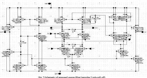
Fig 7 shows the schematic of the channel selection filter with given specification, sizes of MOS, resistors, capacitors. It is designed in virtuoso design environment, using 180nm technology. Library files included is UMC18CMOS technology files, all the components are placed from the same library files. Total of 21 MOS with 5 resistors and 2 capacitor are required with a power supply of 1.8V.
Fig. 7:Schematic of proposed opamp filter (provides 2 pole roll-off)
Fig.8: test bench for simulation of dc, ac&noise analysis Fig. 9: test bench for harmonic balance analysis
The above triangular symbol is the 2 pole opamp circuit which is connected to RC circuit. Two different test benches are designed to analyse the dc, ac and harmonic balance response of the circuit. Linearity, power, area, speed , intermodulation terms, input referred noise is calculated and compared with theoretical results.
Analysis of transfer function and poles :
The filter transfer function is to be derived from fig 8(by writing the KCL equations at the nodes V1 & V2). While considering the opamp open loop gain {A}, we get:
At node V1(non-inverting terminal) applying KCL equations; also we know that V0 = A*Vd
(V1-V0)/R + 2(V1-Vi)/R + (V1-V2)*CS = 0...eq(1)
V1/R + 2V1/R = V0/R + 2Vi/R – Vd*CS (since V1-V2=Vd)...eq(2)
3V1 = V0*(A-RCS) + 2V1*A ...eq(3)
Now applying KCL at node V2 of inverting terminal
(V2-V1)*CS + 2V2/R + V2/R = 0...eq(4)
2V2/R + V2/R = Vd*CS...eq(5)
3V2/R = V0[1/R + CS]...eq(6)
3V2 = V0*[A + RCS ]...eq(7)
Subtracting eq (7) from (3), we will get Vd which can be further replaced by V0 / A
Rearranging the equations in terms of V0 and Vi we get;
Now putting A is equal to infinite; we will get voltage gain as unity, i.e. V0/Vi = 1 which is one the major target which
we have achieved experimentally.
Cutoff frequency: is calculated from eq (9) Fc = 1/RCS ; Putting R = 1K, C = 500f, W = 1000 rad Fc = 2 MHz, which is also proved experimentally.
IV. SIMULATEDRESULTSOFFILTER
Fig.10: filter gain of the 3 pole filter with 0 db(approx)
Filter gain is close to unity and cutoff frequency is 2.03 MHz, both this parameter are equivalent to theoretical values. Gain of a filter should be the same as input signal, only desired band is required to pass the signal. Here band is baseband (generally low frequency band). Fig 10 shows the gain vs frequency curve. In this subsection we limit our analysis to nonlinearities up to the third order, because normally these are the nonlinearities of most interest in a radio environment. For simplicity we further assume that these nonlinearities are memoryless.
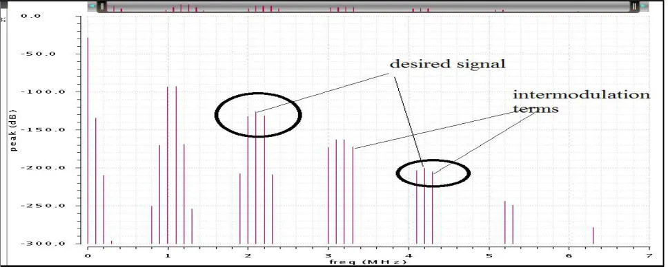
Intermodulation arises when more than one tone is present at the input. A commonmethod for analyzing this distortion is the “two-tone” test. We assume that twostrong interferers occur at the input of the receiver, specified by s(t) = A1cosw1t + A2cosw2t. Here we applied f1 = 1M and f2 = 1.1M. Intermodulation distortion is defined as the ratio of the amplitude of third order harmonics to the amplitude of first order harmonics. So from fig 11 we are getting the desired signal in the frequency f = 1 + 3*1.1 and f = 1 – 3* 1.1. That is f= 4.3MHz and 2.3MHz. Amplitude next to this frequency is first order intermodulation terms and next to this is second order and so on.
Since IM3 depends on input level and is sometimes not as easy to use, we define another performance metric, called the third order intercept point (IP3).
Fig. 12: out of band IIP3 curve Fig. 13: in band IIP3 curve
The intercept point is obtained graphically by plotting the output power versus the input power both on logarithmic scales (e.g., decibels) shown in fig 13. Two curves are drawn; one for the linearly amplified signal at an input tone frequency, one for a nonlinear product.Both curves are extended with straight lines of slope 1 and n (3 for a third-order intercept point). The point where the curves intersect is the intercept point. It can be read off from the input or output power axis, leading to input or output intercept point, respectively (IIP3/OIP3).When comparing systems or devices for linearity, then, a higher intercept point is better. This device with an input-referred third-order intercept point of 14.62dBm is driven with a test signal of −30 dBm. This power is 44.62 dB below the intercept point; therefore nonlinear products will appear at approximately 2x44.62 dB below the test signal power at the device output (in other words, 3×44.62 dB below the output-referred third-order intercept point).
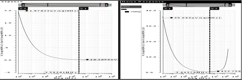
There is circuit noise internal to the subcomponents in the front end. This noise willadd on to the AWGN, cause interference, and further degrade the SNR.Circuit noise is associated with the electricalcomponents that build the subcomponents, such as resistors and MOS transistors. Fig 14 shows the input referred noise is of 1.97 μV which is
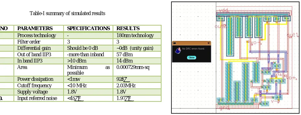
Table-I summary of simulated results
Fig .15: layout of the two pole opamp filter
Fig. 15 shows the layout of the proposed 2 pole roll-off opamp circuit with minimum area of 0.000729 mm-square. It is designed in virtuoso 180nm technology. Minimum poly resistor is used so that the power dissipation is minimum as possible. Microns design rules are kept in mind while designing the layout.
V. CONCLUSION & FUTURE SCOPE
A three pole filter is designed for a wireless receiver using 2 pole roll-off opamp and single pole RC network. We minimized the number of resistors required in the circuit and achieve high linearity, dynamic range, out-band rejection, low input voltage, low power and area. The frequency can be changed by changing R and C in passive network. The cutoff frequency of 2.09 MHz is obtained at this reducing the number of resistor and high out of band linearity is obtained. Work is going on this channel selection filter application to 3G wireless receiver etc. CMFB, transconductance stage, voltage followers are the main key points of the circuits.
REFERENCES
[1] T. Hollman, S. Lindfors, M. Lansirinne, J. Jussila, and K. Halonen, “A 2.7 V CMOS dual-mode baseband filter for PDC and WCDMA,” IEEE J. Solid-State Circuits, vol. 36, no. 7, pp. 1148–1153, Jul. 2001.
[2] M. Oskooei, N. Masoumi, M. Kamarei, and H. Sjöland, “A CMOS 4.35-mW + 22-dBm IIP3 continuously tunable channel select filter for WLAN/WiMAX receivers,” IEEE J. Solid-State Circuits, vol. 46, no. 6,pp. 1382–1391, Jun. 2011.
[3] V. Giannini, J. Craninckx, S. D’Amico, and A. Baschirotto, “Flexible baseband analog circuits for software-defined radio front-ends,” IEEE J. Solid-State Circuits, vol. 42, no. 7, pp. 1501–1512, Jul. 2007.
[4] S. D’Amico, V. Giannini, and A. Baschirotto, “A 4th-order active-Gm-RC reconfigurable (UMTS/WLAN) filter,” IEEE J. Solid-State Circuits, vol. 41, no. 7, pp. 1630–1637, Jul. 2006.
[5] T. Y. LO and C. C. Hung, “Multimode Gm-C channel selection filter for mobile application in 1-V supply voltage,” IEEE Trans. Circuits syst. II, Exp. Briefs, vol. 55, no. 4, pp. 314-318, Apr. 2008
[6] H. A. Alzaher, H. O. Elwan, and M. Ismail, “A CMOS highly linear channel-select filter for 3G multistandard integrated wireless receivers,” IEEE J. Solid-State Circuits, vol. 37, no. 1, pp. 27–37, Jan. 2002.
[7] D. Chamla, A. Kaiser, A. Cathelin, and D. Belot, “A Gm-C low-passfilter for zero-IF mobile applications with a very wide tuning range,”IEEE J. Solid-State Circuits, vol. 40, no. 7, pp. 1443–1450, Jul. 2005.
[8] T. Y. Lo, C. C. Hung, and M. Ismail, “A wide tuning range Gm-Cfilter for multi-mode CMOS direct-conversion wireless receivers,” IEEEJ. Solid-State Circuits, vol. 44, no. 9, pp. 2515–2524, Sep. 2009.
[9] T. Y. Lo and C. C. Hung, “A 1 GHz OTA-Based low-pass filter witha high-speed automatic tuning scheme,” IEEE Trans. Very Large ScaleIntegr. (VLSI) Syst., vol. 19, no. 2, pp. 175–181, Feb. 2010.
[10] A. Liscidini, A. Pirola, and R. Castello, “A 1.25mW 75 dB-SFDRCT filter with in-band noise reduction,” in Proc. IEEE Int. Solid-StateCircuits Conf.-Dig. Tech. Papers, Feb. 2009, pp. 366–367.
[11] T.Y Lo, Chi- Hsiang Lo, “ 1-V 365-μW 2.5 MHz Channel Selection Filter for 3G Wireless Receiver in 55nm CMOS,” IEEE transactions on very large scale integration (VLSI) Systems,vol. 22, no. 5, may 2014.
S.NO PARAMETERS SPECIFICATIONS RESULTS 1. Process technology - 180nm technology
2. Filter order 3 3
3. Differential gain Should be 0 dB ~0dB (unity gain)
4. Out of band IIP3 -more than inband 57 dBm
5. In band IIP3 >10 dBm 14 dBm
6. Area Minimum as
possible
0.000729mm-sq
7. Power dissipation <1mw 927μw 8. Cutoff frequency <10 MHz 2.03MHz
9. Supply voltage 1.8V 1.8V
![Fig. 3:two pole roll-off filter circuit [11]](https://thumb-us.123doks.com/thumbv2/123dok_us/1633253.1203692/3.595.196.419.395.563/fig-two-pole-roll-off-filter-circuit.webp)
![Fig 5. Common mode feedback circuit [8]](https://thumb-us.123doks.com/thumbv2/123dok_us/1633253.1203692/4.595.199.396.449.618/fig-common-mode-feedback-circuit.webp)