International Journal of Advance Research In Science And Engineering http://www.ijarse.com
IJARSE, Vol. No.3, Issue No.9, September 2014 ISSN-2319-8354(E)
403 | P a g e
www.ijarse.com
DESIGN AND IMPLEMENTATION OF AN IMPROVED
QUASI Z SOURCE INVERTER FOR 3 PHASE
INDUCTION MOTOR DRIVE SYSTEMS
D.John Sundar
1, K.R.Shanmugavadivu
2, G.Padmavathi
3, T.Preethika
41, 2, 3
EEE Department, Agni College of Technology, Chennai, (India)
4
PG Student, Agni College of Technology, Chennai, (India)
ABSTRACT
In this paper a new induction motor drive is designed, which provides a single phase to three phase conversion as
well as acts as motor drive. Using effective 4 switch structure and a quasi z-source inverter, voltage boost even
greater than the supply voltage can be achieved. The use of input capacitor in the traditional Z source inverters is
not present in the proposed topology and also the shoot through duty ratio effectively establishes soft switching of
the semiconductor devices. The proposed circuit could also be operated in the bi-directional mode by replacing the
input diode with a bi-directional switch. Since 4 switches instead of the traditional 6 switches are used, the costs of
the circuit along with switching losses are reduced and the control method for this circuit is much simpler than the
traditional 6 pulse circuit.
Keywords
:
Induction Motor Drives , Quazi Z- Source Inverter, Shoot Through Duty Ratio.
I
INTRODUCTION
Three-phase induction motors have been the main consideration in industries more than single phase induction
motors due to certain parameters such as; efficiency, torque ripples and power factor. In places like rural areas to be
use of rolling mills, machine tools and in low power industrial application for robotics, where by a three-phase
utility may not be available, high performance converters must be used to run three-phase induction motor. Low
losses and cost-effectiveness of these converters are very important. [1]
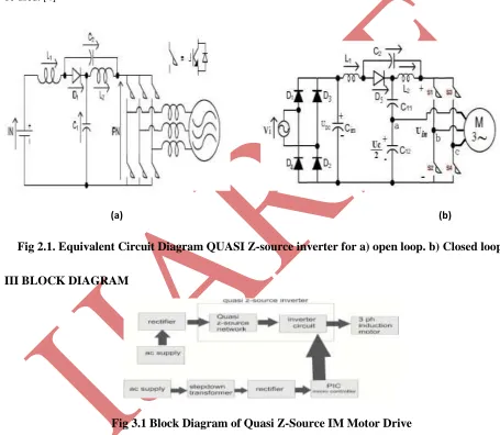
II PROPOSED QUASI Z-SOURCE INVERTER
To solve the aforesaid drawbacks in traditional Z-source inverter, Quasi Z-source inverter(qZSI) topology is used.
The operation principle and merits of the proposed topology is explained in detail, verified using hardware
experiment model and MATLAB simulation is compared with traditional Z-source inverter topology. [1]-[3]
Quasi Z-Source inverters, have been developed which feature several improvements and minimal disadvantages
International Journal of Advance Research In Science And Engineering http://www.ijarse.com
IJARSE, Vol. No.3, Issue No.9, September 2014 ISSN-2319-8354(E)
404 | P a g e
www.ijarse.com
consistent with the voltage fed ZSI, can be made bidirectional by replacing the diode, D1, with a bidirectional
conducting switch.
Also due to the input inductor, L1, the qZSI does not require input capacitance, unlike the ZSI and the qZSI shown
in figure 2.1.b.The qZSI topologies also feature a common dc rail between the source and inverter, unlike the
traditional ZSI circuits. Furthermore, these qZSI circuits have no disadvantages when compared to the traditional
ZSI topologies. These qZSI topologies therefore can be used in any application in which the ZSI would traditionally
be used. [4]
(a) (b)
Fig 2.1. Equivalent Circuit Diagram QUASI Z-source inverter for a) open loop. b) Closed loop.
III BLOCK DIAGRAM
Fig 3.1 Block Diagram of Quasi Z-Source IM Motor Drive
The block diagram of improved Z-source inverter based on the hardware kit model is as shown in the figure 3.1. It
consists of AC supply input voltage of 220v-240v. A step down transformer which is used to step down or decrease
the input AC supply to 12v. Bridge rectifier is used to convert AC supply to DC supply and also regulate DC supply
to 5v. PIC microcontroller is used to generate Pulse Width Modulation (PWM) wave. Driver circuit is used to turn
ON or turn OFF power transistor or MOSFET by giving proper gate signals to respective switches on three legs of
International Journal of Advance Research In Science And Engineering http://www.ijarse.com
IJARSE, Vol. No.3, Issue No.9, September 2014 ISSN-2319-8354(E)
405 | P a g e
www.ijarse.com
or boost operation. The driver circuit signal and signal from Z-source circuit is given to three phase inverter circuit
which converts DC supply to AC supply and then fed to three phase loads.
IV OPERATION PRINCIPLE AND COMPARISON WITH PREVIOUS TOPOLOGY
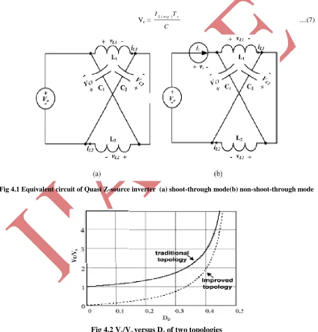
The equivalent circuit of the improved Z-source inverter is shown in 4.1
Assuming that
L1 = L2 = L, C1 = C2 = C ....(1)
When in the shoot-through state, the inverter side is shorted, as shown in we can get
VL = Vo + VC ....(2)
When in the non-shoot-through state , the inverter side can be simplified by an equivalent current source (the current
value is zero when in null state), as shown in . The following equation can be derived in this state:
VL = −V ....(3)
The shoot-through duty ratio is Do and the average value of VL over one switching period is zero, so we can get
VC = Do ....(4)
From this derivation, we can see that in the improved topology, when the shoot-through duty ratio Do is zero, the
Z-source capacitor voltage Vc is equal to zero. When the converter is in the soft-starting state, Vc is zero naturally, so if
we control the Do increase from zero gradually, Vc can also increase from zero gradually and soft start can be
achieved. But this is not the case in traditional topology.
The peak dc-link voltage across the inverter phase legs and peak output phase voltage can be expressed as
Vdc = VC1 + VC2 = VC3 + VC4 = BVin ....(5)
and Vac = M
2 dc V
....(6)
where B =
D 2 1
1
is the boost factor determined by D and M is the modulation ratio. As can be seen from, the
output voltage is boosted by a factor B (B ≥ 1), which is the same as the traditional topology. All the power switches
and diodes used in improved and traditional topologies are exactly the same. A comparison is given on the Z-source
capacitor, Z-source inductor, and input current ripple.
4.1 Z-Source Capacitor Voltage Stress and Voltage Ripple [4]-[5]
The peak dc-link voltage of the two topologies is exactly the same, as can be seen from one can see that the Z-source
capacitor voltage decreases by V0while maintaining the same voltage boost.
The comparison of Vc/Voin the two topologies is shown in figure 4.2.As we already know, the Z-source inverter is
suitable in applications where the input voltage varies in a wide range, such as the battery, fuel cell and photovoltaic
International Journal of Advance Research In Science And Engineering http://www.ijarse.com
IJARSE, Vol. No.3, Issue No.9, September 2014 ISSN-2319-8354(E)
406 | P a g e
www.ijarse.com
Consider, for example, the input voltage is 150–300V. In traditional topology, the capacitor voltage stress is decided
by the maximum input voltage, so VC is no less than 300V. However, in the improved topology, VC is decided by
the minimum input voltage to achieve the maximum voltage boost, the capacitor voltage stress is only 75V to get the
required voltage boost under 150V input voltage; thus, low-voltage capacitors can be used. During shoot-through
time, the condition for previous and improved Z-source inverters is the same, the Z-source inductor current
discharges the capacitors; therefore, the voltage ripple across the capacitors in both inverters can be expressed as
Vc =
C T IL(avg) s
....(7)
Fig 4.1 Equivalent circuit of Quasi Z-source inverter (a) shoot-through mode(b) non-shoot-through mode
International Journal of Advance Research In Science And Engineering http://www.ijarse.com
IJARSE, Vol. No.3, Issue No.9, September 2014 ISSN-2319-8354(E)
407 | P a g e
www.ijarse.com
4.2 Z-Source Inductor Current Ripple
The average Z-source inductor current equals the average input current; therefore, the average Z-source inductor
current in both topologies is the same. For improved topology during the non-shoot-through state, as shown in fig
4.1 (b) the Z-source inductor current decreases and the current ripple can be expressed as
IL = P/Vdc (8)
The input current for a Z-source inverter is different under different controls, and the following analysis will take the
simple boost control as an example. For traditional Z-source inverters, the current to the inverter bridge is ii, so the
input current can be expressed as
iin = 2iL− ii ( 9 )
In shoot-through state, the input current is zero; in traditional zero-state, ii is zero, so iinis 2iL.In active states 1 and 2,
ii is i1 and i2 , respectively, so iinis 2iL − i1 and 2iL − i2 , respectively, and the average input current is IL . Ignoring
the inductor current ripple, iL can be represented as IL.
Fig 4.3 Input current for a.) traditional z-source inverter b.)Quasi z-source inverter
The input current for traditional topology is shown in detail in 4.3.a). The deviation of input current and its average
value can be expressed as For improved topology, the input current is actually the current fed to the inverter bridge,
so in shoot-through state, the input current is 2IL; in traditional zero state, the input current is zero; in active states 1
and 2, the input current is i1 and i2 , respectively, and the averaged input current is IL . The input current for
improved topology is shown in detail in 4.3.b). The deviation of input current and its average value can be
expressed as
International Journal of Advance Research In Science And Engineering http://www.ijarse.com
IJARSE, Vol. No.3, Issue No.9, September 2014 ISSN-2319-8354(E)
408 | P a g e
www.ijarse.com
V SIMULATION AND RESULTS
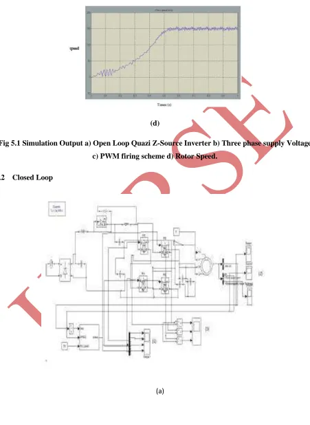
5.1 Open Loop
To confirm the above analysis of impedance source inverter simulation is performed using MATLAB. Fig 5.1
shows the open loop main circuit configuration of impedance source inverter for photovoltaic applications. The
impedance network parameters are L1=L2=1000mH and C1=C2=C=2200mF, switching frequency: 10 kHz. The
purpose of the system is to boost the input voltage and rotor speed characteristics is shown in fig 5.1.d
(a)
International Journal of Advance Research In Science And Engineering http://www.ijarse.com
IJARSE, Vol. No.3, Issue No.9, September 2014 ISSN-2319-8354(E)
409 | P a g e
www.ijarse.com
(d)
Fig 5.1 Simulation Output a) Open Loop Quazi Z-Source Inverter b) Three phase supply Voltage
c) PWM firing scheme d) Rotor Speed.
5.2 Closed Loop
International Journal of Advance Research In Science And Engineering http://www.ijarse.com
IJARSE, Vol. No.3, Issue No.9, September 2014 ISSN-2319-8354(E)
410 | P a g e
www.ijarse.com
(b) (c)
Fig 5.2 a) Simulation Block of Closed Loop qZSI. b) Simulation Output of PWM firing scheme
and c) Controlled Rotor Speed
The main circuit configuration of impedance source inverter is shown in figure 5.2. The impedance network
parameters are L1=L2=1000 microHenry and C1=C2=C= 2200microFarad, switching frequency: 10 kHz.
The purpose of the system is to boost the input voltage. The simulation model consists of two parts. One is main
system and the other one is subsystem. Main system is used to produce PWM wave by comparing sine wave and
oscillatory wave and is given to the subsystem.
PI controller is used for the closed loop control of the quasi Z-source inverter reference speed is given to the
controller and the actual speed is given using the speed sensing unit. The pulse triggers are generated from the above
controller using the pi controller. The output pulses are given to the four MOSFET switches. The rotor speed
relationship with time is shown in the figure 5.4
VI HARDWARE CIRCUIT BOARD
The Hardware kit for Improved Z-source Inverter is as shown in the above figure 6.1. The Hardware Circuit Board
consists of following main parts :230/12V Step DownTransformer ,Rectifier circuit, Controller circuit, Driver
circuit, Z-source Impedance circuit
The 230/12v step down transform is used to step down the input ac supply voltage of 230V given in the primary coil
is step down to 12v ac supply. The output voltage is taken from secondary coil. In this transformer the primary coil
winding is greater than secondary coil winding. These coils are wound over the laminated iron core. The rectifier
circuit is used to convert 12 ac supply to 12v dc supply. It also consists of a capacitor, four diodes, voltage regulator,
a LED bulb. Voltage regulator is used to convert 12v dc supply to 5v constant dc supply and it is as shown the figure
International Journal of Advance Research In Science And Engineering http://www.ijarse.com
IJARSE, Vol. No.3, Issue No.9, September 2014 ISSN-2319-8354(E)
411 | P a g e
www.ijarse.com
Fig.6.1 Hardware Circuit Board
The LED bulb is used to give indication whether the rectifier circuit is working or not. A voltage regulator is used
for converting pulsating dc to fixed dc. A PIC microcontroller shown in fig 6.1.is used for the generation of the
trigger pulse. This is achieved using the sinusoidal pulse width modulation from which the output is given to the
driver circuit for amplification and optical isolation. In electronics, driver is an electrical circuit or other electronic
component used to control another circuit or other component, such as a power MOSFET or high-power transistor.
The term is used, for example, for a specialized computer chip that controls the high-power transistors in DC-to-DC
voltage converters. The Driver circuit diagram is as shown in the Fig 6.5.In this three driver circuit are used for
switching operation of six MOSFET. Each driver circuit controls switching operation for two MOSFET. For this
purpose IR2110 IC is used. The IR2110 is a high voltage, high speed power MOSFET driver with independent high
and low side referenced output channels. The circuit board diagram of z-source is as shown in the figure 6.1. It
consists of two inductors of value 1000microHenry and two capacitors of value 2200 micro Farad.
VII CONCLUSION
A 220v to 50 volt transformer is used in the input side. A tachometer is used for check in the speed of the motor.
A half hp squirrel cage induction motor is used for verification of the result. A multi meter is used for checking
the output voltage. The input voltage is found to be 50V AC while the output is 3 phase 58V. This is sufficient to
drive a 3 phase induction motor with a speed of 900 rpm. The future scope of this paper can be extended for the
use in rural areas where 3 phase supply is in high demand. Closed loop of this paper is simulated which can be
implemented in places where constant speed is required. It can also be used with DC supply by directly
International Journal of Advance Research In Science And Engineering http://www.ijarse.com
IJARSE, Vol. No.3, Issue No.9, September 2014 ISSN-2319-8354(E)
412 | P a g e
www.ijarse.com
REFERENCE
[1] F. Z. Peng, (, March/April 2003) “Z-Source Inverter,” IEEE Transactions on Industry Applications, vol. 39,
No. 2, pp. 504-510.
[2] F. Z. Peng,( 2004)“Z-Source Inverter for Motor Drives,” in Proc.IEEE PESC’04, pp. 249-254.
[3] Peng, F.Z.; Xiaoming Yuan; Xupeng Fang; ZhaomingQian;(June2003)“Zsourceinverte for adjustable sped drives”IEEE PoweElectronics Letters,Volume: 1 , Issue: 2 , pp:33 – 35.
[4] MiaosenShen, Jin Wang, Alan Joseph, FangZ.Peng,LeonM.Tolbert,andDonald, J.Adams,(2004)“Maximum
constant boost control of the Z-source inverter” in Proc. IEEE IAS’04, p.142.
[5] F.Z. Peng, M. Shen, and Z. Qian, “Maximum boost control of the Z-source inverter” in Proc. IEEE PESC’04,