Enhancing the Bandwidth of a Microstrip Patch Antenna at 4
GHz for WLAN using H-shaped Patch
Md. Khaliluzzaman1, Deepak kumar Chy.2 and Md. Rezanul Haque Chowdhury3
1Department of Computer Science & Engineering, University of Information Technology & Sciences (UITS),
Dhaka, Bangladesh.
2
Department of Electrical & Electronic Engineering, University of Information Technology & Sciences (UITS), Dhaka, Bangladesh.
3Senior Engineer, Division of IT, KDS Industries Ltd.,
Chittagong, Bangladesh.
Abstract
This paper presents A H-shaped wide band micostrip patch antenna at 4 GHz for WLAN applications. Performance is improved by inserting a pair of slits in an appropriate radiating edge to form H-Shaped patch antenna. The proposed antenna designed in this paper exhibits enhanced bandwidth with multi resonant frequencies. In this work a geometric H-shaped is developed from a rectangular patch of the width (W=29.6 mm) and length (L=24.5 mm). The antenna was fabricated using Rogers RT-5880 substrate with a dielectric constant εr of 2.2 and a thickness of 1.574 mm respectively. The result of proposed antenna was obtained in terms of Return Loss and bandwidth. The simulated result shows that the H-shaped patch antenna has the highest bandwidth in comparison with Parasitic patch antenna, Stacked patch antenna, Proximity coupled patch antenna and E-shaped patch antenna.
Keyword: Microstrip patch antenna, WLAN, Rogers RT-5880
Substrate, dielectric constant, return loss.
1. Introduction
Communication can be broadly defined as the transfer of information from one point to another. A communication system is usually required when the information is to be conveyed over a distance.
The term “Microstrip” comes because the thickness of this metallic strip is in micro-meter range. Microstrip patch antennas are popular, because they have some advantages due to their conformal and simple planar structure.
With the increase in data rates and a trend of miniature electronic circuits for wireless digital applications, the antennas required for these applications should be light weight, easily mountable and have a broad bandwidth [1]-[3]. These requirements can be met by using microstrip antennas and patch arrays. Balanis [6] states that an antenna should be low profile, simple and
inexpensive to fabricate and it should be easy to mount on planar and non-planar surfaces. When the type of patch to be used for an application is chosen, the dimensions should be carefully analyzed. A small change in any dimension can cause a noticeable change in the results e.g., the frequency, impedance matching, bandwidth, directivity and gain etc. Microstrip single element antenna has advantages but it also has several disadvantages, such as low efficiency, narrow bandwidth, low gain and directivity. These disadvantages can be overcome by using multiple patch elements in different configurations called patch arrays.
The most fundamental form of a Microstrip Patch antenna consists of a radiating patch on one side of a dielectric substrate which has a ground plane on the other side as shown in Fig. 1. The patch is generally made of conducting material such as copper or gold and can take any possible shape. The radiating patch and the feed lines are usually photo etched on the dielectric substrate.
The remaining paper is organized as follows. In section II, Design Methodology is described. In section III, Antenna Design and Analysis is explained and simulation results are given in section IV. The paper is concluded in section V.
Fig. 1. Structure of Microstrip Patch Antenna.
2. Design Methodology
Microstrip patch antennas consist of very thin metallic strip (patch) placed on ground plane where the thickness of the metallic strip is restricted by t<< λ0 and the height is restricted by 0.0003λ0 ≤ h ≤ .05λ0 [4, 5] where λo is the free space wavelength. The microstrip patch is designed so that its radiation pattern maximum is normal to the patch. For a rectangular patch, the length L of the element is usually λ0/3 <L< λ0 /2.
There are numerous substrates that can be used for the design of microstrip antennas and their dielectric constants are usually in the range of 2.2 ≤ εr ≤12. To implement the microstrip antennas usually Fr-4 (εr = 4.9), Rogers TMM 4(εr = 4.5), Taconic TLY-5 (εr = 2.2), Alumina (96%) (εr = 9.4), Teflon(PTFE) (εr = 2.08), Arlon AD 5 (εr = 5.1) dielectric materials are used as the substrate [5,7,9].
The Performance of the microstrip antenna depends on its dimension. Depending on the dimension the operating frequency, radiation efficiency, directivity, return loss and other related parameters are also influenced [4].
2.1 Design Equation
For an efficient radiation a practical width of the microstrip patch element becomes [3, 5, 9]
W = (1)
And the length of the antenna becomes [2, 4, 5]
(2)
Where,
(3)
And
(4)
Where, λ is the wave length, ƒr (in Hz) is the resonant frequency; L and W are the length and width of the patch element, in mm, respectively and εr is the relative
dielectric constant.
The most serious limitation of the microstrip antenna is its narrow BW. The bandwidth could be defined in terms of its VSWR or input impedance variation with frequency or in terms of radiation parameters. For the circularly polarized antenna, bandwidth is defined in terms of the Axial Ratio. VSWR is a very popular parameter for
determining the bandwidth of a particular antenna configuration (1≤ VSWR ≤ 2) as an acceptable interval
for determining the bandwidth of the antenna. Bandwidth is presented more concisely as a percent;
(5)
Where ∆f is the width of the range of acceptable frequencies, and fr is the resonant frequency of the
antenna [12].
The BW of the MSA can be inversely proportional to its quality factor Q and is given by [6].
(6)
The BW is usually specified as frequency range over which VSWR ≤ 2. However, in recent years considerable effort has been spent to improve the bandwidth of the microstrip antenna, in part by using alternative feeding schemes [11].
The return loss is another way of expressing mismatch. It is a logarithmic ratio measured in dB that compares the power reflected by the antenna to the power that is fed into the antenna from the transmission line. The relationship between VSWR and return loss is as follows [10].
(7)
3. Antenna Design and Analysis
The goal of designing a microstrip antenna at 4 GHz was to improve bandwidth and directivity for the WLAN application. There are various important steps in designing microstrip antennas. The most important one is choosing the right kind of substrate. Different substrates can be used to fabricate an antenna with a good response. The dielectric constants of the substrates lie in the range of 2.2 ≤ r ≤ 12. Usually the substrate chosen for the antenna design is thick and has a dielectric constant on the lower end. This provides better performance in contrast to thin substrates with higher dielectric constants [8]. FR-4 and Rogers RT5880 was available for fabrication, since FR-4 has higher losses and has higher dielectric constant, Rogers RT5880 was chosen for fabrication and simulation purpose. The width of the rectangular patch antenna is usually chosen to be larger than the length of the patch, L to get higher bandwidth. To design patch antenna lower dielectric constant is used because in case of lower dielectric constant of the
substrates, surface wave losses are more severe and dielectric and conductor losses are less severe.
Once the single element antenna was designed and simulated then the array configuration performance evaluation was carried out. Table 1 shows the specifications for the proposed microstrip patch antenna. Table 1: Design Specification for antenna
Substrate Rogers RT5880
Center Frequency (fr) 4 GHz Height of Substrate (h) 1.574 mm
Loss Tangent 9 x 10⁻⁴
Dielectric Constant ( r) 2.2
Copper Thickness 0.035mm
Width of the patch (W) 29.6 mm Length of the patch (L) 24.5 mm
This section describes the design of a H-shaped microstrip patch antenna. The most important design features of the patch are its width (W), length (L), width of transmission line and the length of the feeding line. These specifications are dependent on each other as well as the frequency of operation. Different equations given in Eq.(1) to (4) were used to calculate the patch dimensions i.e., W and L: The patch was fed by a 50 Ω discreet port. The H-shaped microstrip patch design in shown in Fig. 2.
4. Simulation and Result
The proposed antenna is to be used for the wireless local area network (WLAN). The antenna is to operate in the frequency range from 3GHz to 5.5GHz. The dielectric material selected is Rogers RT5880 which has a dielectric constant of 2.2. A thick dielectric substrate having a low dielectric constant is selected for better efficiency, larger bandwidth and better radiation .The
objective is to get an improve bandwidth from the conventional microstrip patch.
In this design, we have proposed H-shape patch antenna of width (W) = 29.6 mm and length (L) =24.5 mm. The proposed antennas are simulated using SONNET software, under the same conditions and results compared with the conventional parasitic patch antenna, proximity coupled patch antenna, stacked patch antenna and E-shaped patch antenna, and the shape with improve bandwidth is adopted, and implemented. The bandwidth was obtained where return loss is less than -10dB which is an acceptable level to describe the loss of the power which reflects back from the antenna without being radiated. Fig. 2 shows the geometry of H-shaped microstrip antenna (MSA). The antenna is designed for the operating frequency of 4GHz. It consists of radiating patch of length L and width W.
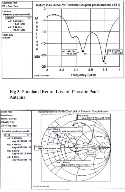
Fig. 3, Fig. 4 and Fig. 5 show the simulated result of return losses, Input impedance curve and current density diagram of parasitic patch type antenna respectively.
Fig 3. Simulated Return Loss of Parasitic Patch Antenna.
Fig4. Input Impedance Curve of Parasitic Patch Antenna.
29.6mm
24.5mm
Fig. 2. H-shaped patch antenna.
In Fig. 5, the input impedance curve has shown us the magnitude and phase angle of the input impedance of the antenna at the respective frequencies. It is also possible to estimate the bandwidth of the antenna from this graph by reading the frequencies at the points where the VSWR (Voltage Standing Wave Ratio) = 2 circle and the input impedance curve intersect.
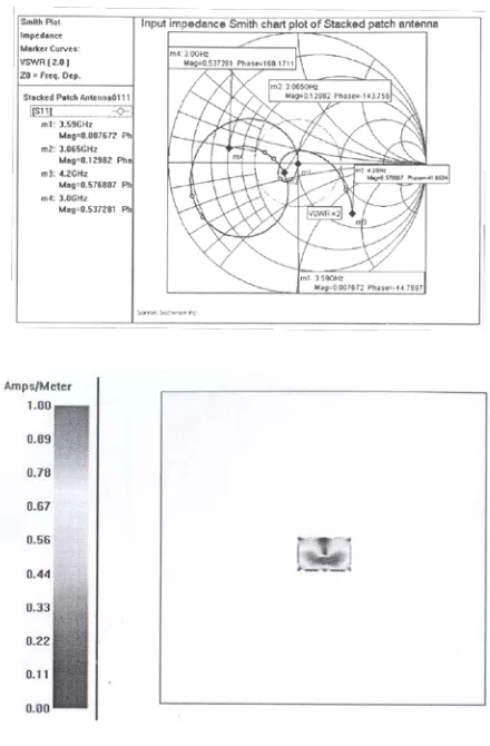
The following simulated results are obtained for the stacked patch type antenna. The results are explained in terms of the return loss, input impedance in Figure 6 and Fig. 7. The current density on the antenna is also displayed in Fig. 8.
The return loss, input impedance and current density diagram for proximity coupled antenna are shown in Fig. 9, Fig. 10, Fig. 11 and for E-shape patch antenna are shown in Fig. 12, Fig. 13, Fig. 14 respectively.
Fig 5. Current density diagram of the parasitic patch antenna at 3.845 GHZ
Fig 6. Simulated Return Loss of Stacked Patch Antenna.
Fig 7. Input Impedance Curve of Stacked Patch Antenna.
Fig 8. Current density diagram of the stacked patch antenna at 3.285 GHZ
Figure 9. Simulated Return Loss of Proximity Coupled Patch Antenna.
The proposed H-shape antenna in terms of return loss, input impedance and current density diagram are shown in Figure 15, Figure 16, Figure 17
Fig 10. Input Impedance Curve of Proximity Coupled Patch Antenna.
Fig 11. Current density diagram of the proximity coupled patch antenna at 3.485 GHZ
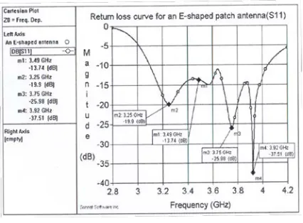
Fig 12. Simulated Return Loss of E-shaped Patch Antenna.
Fig 13. Input Impedance Curve of E-shaped Patch Antenna.
Fig14. Current density diagram of the E-shaped patch antenna at 3.44 GHZ
Fig 15. Simulated Return Loss of H-shaped Patch Antenna.
From the graph, the experimental bandwidth is calculated using the formula
(8)
Where, 𝑈𝑈𝑓𝑓 and 𝐿𝐿𝑓𝑓 are upper and lower cut-off frequencies of the bandwidth respectively when its return loss reaches -10dB and 𝐶𝐶𝑓𝑓 is the resonant frequency between 𝑈𝑈𝑓𝑓 and 𝐿𝐿𝑓𝑓.
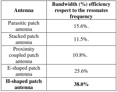
We have observed from Fig. 3 that the bandwidth obtained using Parasitic patch antenna is 15.6% of the resonant frequency which is about 560 MHz, where as in Fig. 6, Fig. 9 and Fig. 12 for Stacked patch antenna, Proximity coupled patch antenna and E-shaped patch antenna bandwidth found to be 11.5%, 10.8% and 25.6%
of the resonant frequency which are about 550 MHz, 400 MHz and 950MHz.
On the other hand Fig. 15 shows the variation of return loss versus frequency of out proposed H-shape patch antenna. The antenna resonates at two bands of frequencies at 4.2GHz and 4.3GHz. The overall bandwidth is 38% of the resonant frequency that is about 1.6 GHz.
The bandwidths of four types of patch antennas and our proposed H- shaped patch antenna with respect to the resonates frequency are given below.
Table 2: Bandwidth (%) efficiency in term of resonates frequency
Antenna
Bandwidth (%) efficiency respect to the resonates
frequency
Parasitic patch
antenna 15.6%.
Stacked patch
antenna 11.5%.
Proximity coupled patch
antenna
10.8%.
E-shaped patch
antenna 25.6%
H-shaped patch
antenna 38.0%
5. Conclusions
A H-shaped microstrip patch antenna at 4 GHz for WLAN application was designed and tested using SONNET simulator. The H-shaped Microstrip patch antenna performance was then improved in terms of thickness of the dielectric substrate, the size of the metallic patch, the dielectric constant of the dielectric substrate, the feed type to be used (as seen in the non-contacting feed techniques) and the coupling level to some extent. The proposed H-shape patch antenna performs better than those of conventional patch antennas, which is approximately 38% of bandwidth efficiency in terms of resonant frequency.
Fig 16. Input impedance curve of H-shaped Patch Antenna.
Fig 17. Current density diagram of the H-shaped patch antenna at 3.5 GHZ
References
[1] P. Pigin, Emerging mobile WiMax antenna technologies, IET Communication Engineer, October/ November 2006.
[2] C.Y Pan, T. S Horng, W. S Chen and C.H Huang, Dual wideband Printed Monopole Antenna for WLAN/WiMax Applications, IEEE Antenna and Wireless Propagation letters, vol 6, pp. 149-151, 2007. [3] Y. Yu, Y. Lee, S. Lee and J. Choi, A compact internal
antenna for wireless USB Dongle application, in Proc. ICAT 2009, pp. 1084-1086.
[4] T. A. Millikgan, Modern Antenna Design, 2nd ed. , IEEE Press, John Wiley & Sons inc., 2007.
[5] M. I. Skolnik, Introduction to RADAR System, 3rd ed., McGraw Hill Higher Education, 2000.
[6] C. A.Balanis, Antenna Theory, 2nd. Edition ed. Arizona State University: John Wiley & Sons,Inc., 1997. pp. 722-723.
[7] R. J. Mailloux, J. F. Mcllvenna, N. P. Kernweis, “Microstrip array technology”, IEEE Trans. Antenna Propagation Magazine, Vol. 29, No. 1, pp. 25-27, 1981. [8] H.Y.D. Yang, Miniaturized printed wire antenna for
wireless communications, IEEE Antennas Wireless Propag. Lett., vol. 4, pp. 358-361,2005.
[9] C. A. Balanis, Antenna Engineering, 2nd ed., Willey, 1982.
[10] http://wireless.ictp.it/handbook/C4.pdf.
[11] D. R Jackson and J .T Williams, “A comparison of CAD models for radiation from rectangular microstrip patch,” Intl. Journal of microwave and millimeter-wave computer Aided Design, vol 1, no.2 pp.236-248, April 1991.
[12] I. J. Bahl and P. Bhartia, “Microstrip Antenna” Artech House, 1980.
[13] M. F. Islam, M. A. Mohd. Ali, B. Y. Majlis and N. Misran, “Dual Band Microstrip Patch Antenna for Sar Applications”, Australian Journal of Basic and Applied Sciences, 4(10): 4585- 4591, 2010.
[14] K. P Ray, “Broadband, dual-frequency and compact microstrip Antennas” Ph.D Thesis, Indian Institute of Technology, Bombay, India, 1999.
Md. Khaliluzzaman received the B.Sc (Engg) degree in Computer Science & Engineering from Khulna University of Engineering & Technology (KUET) in 2007. Now he is continuing his Post graduation in Chittagong University of Engineering & Technology (CUET). He is now working as a faculty member in Computer Science & Engineering Department at University of Information Technology & Sciences (UITS). His current research interests are in the area of Digital Image Processing, Computer Vision, Pattern Recognition, Wireless Communication, Networking, Antenna and Wireless network Security.
Deepak Kumar Chy. received the B.Sc (Engg) degree in Electrical & Electronics Engineering from Chittagong University of Engineering & Technology (CUET) in 1998 and received his MSc in CSCE from University of Duisburg-Essen,Germany. He is now working as a faculty member in Electrical & Electronics Engineering Department at University of Information Technology & Sciences (UITS). His current research interests are in the area of Signal Processing, Wireless
Communication, Networking, Antenna, Digital Image Processing and Wireless Network Security.
Rezanul Haque Chowdhury received the B.Sc (Engg) degree in Computer Science and Engineering from BGC Trust University. He is now working as a senior engineer at KDS industries Ltd. His current research interests are in the area of Digital Image Processing, Antenna and Wireless Network Security.