Digital PWM Controller for Multilevel
Inverter
using FPGA Technique
V.S.Priscilla
1, Jasmine*
2Assistant Professor, Dept. of ECE, Jerusalem College of Engineering, Chennai, Tamil Nadu, India1 Assistant Professor, Dept. of ECE, Bharath University, Chennai, Tamil Nadu, India2
*
Corresponding Author
ABSTRACT: A single-phase five-level photovoltaic (PV) inverter topology for grid-connected PV systems with a novel pulse width-modulated (PWM) control scheme is proposed. Two reference signals identical to each other with an offset equivalent to the amplitude of the triangular carrier signal were used to generate PWM signals for the switches. The inverter offers much less total harmonic distortion and can operate at near-unity power factor. The proposed system is verified through simulation and the results are compared with that with the conventional single-phase three-level grid-connected PWM inverter. A six-switch topology inverter with symmetrical Pulse Width Modulation (PWM) switching technique is used. A low pass filter is incorporated in the circuit to filter out unwanted harmonics and produce a sinusoidal AC current. FPGA is the device which holds the advantages of both, high-speed operation which is feature of the hardware and adaptability which is feature of the software.
I. INTRODUCTION
Multilevel inverters have been attracting increasing attention in the past few years as power converters of choice in many applications. They have significant advantages over the conventional one because of the capability to reduce the undesirable harmonics in order to improve the performance and efficiency. Various topologies to realize these inverters have been introduced and studied recently. Waveform synthesis methods for these inverters include staircase modulation, sine-triangle carrier modulation, space vector modulation and other predictive methods.
Normally the topological structure of multilevel inverter suggested must cope with the following points: 1) It should have less switching devices as far as possible, 2) It should be capable of enduring very high input voltage such as HVDC transmission for high power applications, and 3) Each switching device should have lower switching frequency owing to multilevel approach [4]. PWM generation is considered the more important in the inverter design and several multicarrier techniques have been developed to reduce the distortion in multilevel inverters, based on the classical (SPWM) with triangular carriers. Some methods use carrier disposition and others use phase shifting of multiple carrier signals. Xilinx field programmable gate arrays (FPGA's) are standard integrated circuits that can be programmed by a user to perform a variety of complex logic functions.
II. PROPOSED SYSTEM CONFIGURATION
For the conventional single-phase three-level capacitor clamped inverter, there are four power switches and one flying capacitor in each leg to generate three voltage levels on the ac side [1-2]. The voltage stress of active switches is equal to half the dc bus voltage. The control scheme of this circuit configuration is complicated. The proposed single-phase three-level inverter is shown in Figure 1 to reduce one flying capacitor and to make the control scheme easy. Four power switches and one flying capacitor are used in the leg-a to generate a three-level PWM waveform on the voltage Van. The flying capacitor voltage V2 is equal to half the dc bus voltage (V2=Vdc/2) [3].
There are four active switches with voltage stress Vdc/2 in the leg-b to generate a two-level PWM waveform on the
voltage Vbn. Power switches in the leg-b are operated at low switching frequency (60Hz) [16]. By the proper control, a
five-level PWM voltage waveform is generated on the ac terminal voltage Vab . There are eight power switches and one
clamped capacitor in the adopted three-level inverter.
Fig.1 The proposed circuit of the multilevel PWM single phase inverter
Power switches have the following relationship to prevent the damage of active switches in the adopted inverter Sxy + Sxy’ = 1 ………. (1)
Where Sxy (or Sxy’) =1 if switch Sxy (or Sxy’) is turned on, or Sxy (or Sxy’) =0 if switch Sxy (or Sxy’) is turned off, x=a and
b, y=1 and 2. In the inverter leg-b, the PWM signals for power switches are Sb1=Sb2 and Sb1’=Sb2’. Thus there are only
three independent power switches Sa1, Sa2 and Sb1 in the proposed inverter [5], [17]. All elements are assumed ideal and
the output voltage is constant during one switching period. The capacitor voltages V1 and V2 are assumed to be
V2=V1/2=Vdc/2. According to the switching states of these three independent switches, there are eight valid switching
states as shown in Table 2. Depending on the voltage level, there is one operating state to generate voltage Vab=Vdc and
-Vdc, respectively, two operating states to achieve voltage Vab=Vdc/2, 0 and -Vdc/2, respectively. According to the
voltage level of ac terminal voltage Vab, the operation of the adopted inverter can be classified into five operating
Table 1. Valid switching states of the proposed voltage source inverter output voltage
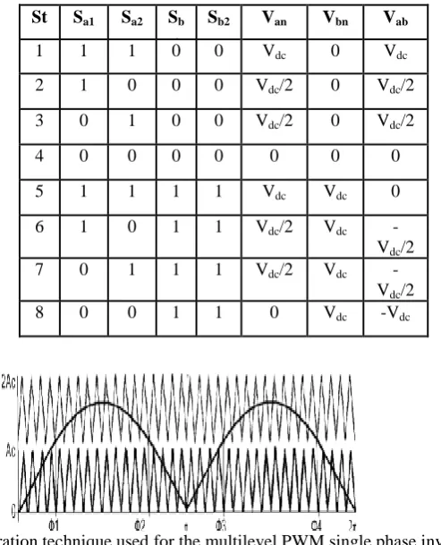
Fig.2 PWM generation technique used for the multilevel PWM single phase inverter. The parameters of the modulation process are shown in Fig.2 and defined as following:
1) The modulation index is defined as:
Where Am is peak value of sinusoidal wave and Ac is the peak is the carrier peak-peak value. 2) The frequency modulation index:
Where the frequency of the carrier is wave and is the frequency of the sinusoidal wave.
3) The angle of displacement existing between the sinusoidal wave and the first positive carrier wave can be defined as following:
St Sa1 Sa2 Sb
1
Sb2 Van Vbn Vab
1 1 1 0 0 Vdc 0 Vdc
2 1 0 0 0 Vdc/2 0 Vdc/2
3 0 1 0 0 Vdc/2 0 Vdc/2
4 0 0 0 0 0 0 0 5 1 1 1 1 Vdc Vdc 0
6 1 0 1 1 Vdc/2 Vdc -
Vdc/2
7 0 1 1 1 Vdc/2 Vdc -
Vdc/2
III. PWM GENERATION USING XILINX FPGA
Fig.3 The block diagram of single phase PWM generator in XILINX FPGA
The upper and lower carrier waves (1800 Hz) are compared with the sinusoidal wave (50 Hz). In same time a pulse signal has frequency of (50 Hz) is generated and inverted to get its inverse pulse signal [8], [12].
There are only three control signals S6, S5 and S2 will be needed to derive, another three S3, S1, and S4 are simply generated in method of the logical inverse of S6, S5, and S2 respectively as shown in fig.4.
Fig.4 Single phase PWM scheme generator in XILINX FPGA
3.1 Sinusoidal Wave Generation
The schematic diagram of the sine wave consists of a memory Pointer unit and schematic block includes a VHDL program for sine wave data as shown in Fig.3. The VHDL program includes 19 sine wave data calculated at every 5° degrees, these data cover quarter cycle of sine wave 90° degrees [6-7].
As the modulation index depends on the modulation wave amplitude, the sine wave data can be changed to achieve the required modulation index and thus the required output voltage [13-15].
3.2 Carrier Wave Generation
Where is the main clock frequency, is the carrier (upper and lower) wave frequencies and n is the bit size of the up-down counter [9].
3.3 Pulse Signal 50Hz Generation
Two inverse pulse signals have same frequency (50Hz) need to be generated; their frequencies are similar to the sinusoidal wave and the output frequency [10]. Pointer unit consists of an 8 bit counter, some logic gates and VHDL program developed to store data in term of condition statements are the main structure of the pulse signal (50 Hz). These two signals have two functions, first as a switching signal for switches S4 and S2, second to involve with the resultant signals produced from comparators to generate the appropriate switching signals for switches S6, S3, S5 and S1 [11].
3.4 PWM Distribution Unit
This unit is used to distribute the PWM output pattern to the switches (S1, S2, S3, S4, S5 and S4). The distribution unit consists of a few logic gates (AND, OR, and NOT) deal with the three main signals produced from comparators and pulse signals 50 Hz generation unit to form the final PWM as shown in Fig.4.
IV. SIMULATION RESULTS
The proposed capacitor clamped inverter is simulated using software package PSIM 6. The main components of proposed inverter are: C1=2200µF, C2=330µF, Co=18uF, Lo=1mH and Vo, rms=110V/60Hz. The capacitor voltage V2
equals 100V. The dc bus voltage is 200V. The triangular carrier frequency is 20 kHz. The figure 6.1 shows the simulated circuit diagram of the proposed inverter.
Fig.6 Simulation result for PWM generation.
V. CONCLUSION
A single-phase voltage source inverter based on capacitor clamped configuration is proposed to provide a sinusoidal voltage to the output load. Three-level PWM scheme is used in the proposed inverter to reduce voltage harmonics on the ac side and reduce the voltage stress of the power semiconductors. The voltage stress of power devices is clamped to half the dc-link voltage.
Power switches in the one leg of inverter are operated at low switching frequency to generate two voltage levels on the voltage. Power switches in another leg of inverter are operated at high switching frequency to generate three voltage levels on the ac side voltage. Five voltage levels are achieved on the ac line output voltage.
REFERENCES
1. A. Nabae, I. Takahashi, and H. Akagi, 1981, “A new neutral point-clamped PWM inverter,” IEEE Transactions on Industry Applications, vol. 19,no. 5, pp. 518-523.
2. J. S. Lai and F. Z. Penf, 1996, “Multilevel converters – a new breed of power converters,” IEEE Transactions on Industry Applications, vol. 32, no. 3.
3. Jeyanthi Rebecca L., Dhanalakshmi V., Sharmila S., "Effect of the extract of Ulva sp on pathogenic microorganisms", Journal of Chemical and Pharmaceutical Research, ISSN : 0975 – 7384 , 4(11) (2012) pp.4875-4878.
4.M. Marchesoni, M. Mazzucchelli ans S. Tenconi, 1992, “A non conventional power converter for plasma stabilization,” in Proc. IEEE Power Electronics Specialist Conference, 1988, pp. 122-129.
5. J. Steinke, “Switching frequency optimal PWM control of a three level inverter,” IEEE Transactions on Power Electronics, vol. 7, no. 3, pp. 487-496.
6. Sharmila S., Rebecca L.J., Saduzzaman M., "Effect of plant extracts on the treatment of paint industry effluent", International Journal of Pharma and Bio Sciences, ISSN : 0975-6299, 4(3) (2013) pp.B678-B686.
7. L. M. Tolbert, F. Z. Peng and T. G. Habetler, 1999, “Multilevel PWM methods at low modulation indices,” in Proc. IEEE Applied Power Electronic Conference,
9. Shanthi B., Revathy C., Devi A.J.M., Subhashree, "Effect of iron deficiency on glycation of haemoglobin in nondiabetics", Journal of Clinical and Diagnostic Research, ISSN : 0973 - 709X, 7(1) (2013) pp.15-17.
10. T. A. Meynard and H. Foch, 1992, “Multilevel conversion: High voltage choppers and voltage source inverter,” in proc. IEEE Power Electronics Specialist Conference, pp. 397-403.
11. X. Yuan, H. Stemmler and I. Barbi, 1999, “Investigation on the clamping voltage self-balancing of the three-level capacitor clamping inverter,” in proc. IEEE Power Electronics Specialist Conference, pp. 1059- 1064.
12. Rayen R., Hariharan V.S., Elavazhagan N., Kamalendran N., Varadarajan R., "Dental management of hemophiliac child under general anesthesia", Journal of Indian Society of Pedodontics and Preventive Dentistry, ISSN : 0970-4388, 29(1) (2011) pp.74-79.
13. X. Yuang; H. Stemmler and I. Barbi, 2001, “Self-balancing of the clamping-capacitor-voltages in the multilevel capacitor- clamping inverter under sub-harmonic PWM modulation,” IEEE Transactions on Power Electronics, vol. 16,
14. C. Turpin, L. Deprez, F. Forest, F. Richardeau, and T. A. Meynard, 2002, “A ZVS imbricated cell multilevel inverter with auxiliary resonant commutated poles,” IEEE Transactions on Power Electronics, vol. 17,no. 6, pp. 874 –882.
15. Menon R., Kiran C.M., "Concomitant presentation of alopecia areata in siblings: A rare occurrence", International Journal of Trichology, ISSN : 0974-7753, 4(2) (2012) pp.86-88.
16. B.R Lin, C.H Huang, September 2004 “analysis and implementation of a single phase capacitor –clamped inverter with simple structure,” IEE Proc-Electr.Power Appl, vol 151, no5, pp. 555-560.
17. S.-G. Lee, D.-W. Kang, Y.-H. Lee and D.-S. Hyun, 2001, “The carrier based PWM method for voltage balance of flying capacitor multilevel inverter,” in Proc. IEEE Power Electronics Specialists Conference, pp. 126 –131.
18. B Karthik, TVUK Kumar, Noise Removal Using Mixtures of Projected Gaussian Scale Mixtures, World Applied Sciences Journal, 29(8), pp 1039-1045, 2014.
19. Daimiwal, Nivedita; Sundhararajan, M; Shriram, Revati; , Non Invasive FNIR and FMRI system for Brain Mapping . 20. Daimiwal, Nivedita; Sundhararajan, M; , Functional MRI Study for Eye Blinking and Finger Tapping.
21. Shriram, Revati; Sundhararajan, M; Daimiwal, Nivedita; , Effect of change in intensity of infrared LED on a photoplethysmogramIEEE Communications and Signal Processing (ICCSP), 2014 International Conference on, PP 1064-1067,2014.
22. Kanniga, E; Srikanth, SMK; Sundhararajan, M; , Optimization Solution of Equal Dimension Boxes in Container Loading Problem using a Permutation Block AlgorithmIndian Journal of Science and Technology, V-7, I-S5,PP 22-26, 2014.