ABSTRACT: Memories of Flash are another type of memory of non-volatile on floating-gate transistors. The use of commodity and embedded memories of flash has rapid growth while we are entering in the system-on-chip era. Conventional tests for flash memories are usually ad hoc is the test procedure which is developed for a specific design. As there is a large number of possible failure modes for memories of flash, algorithms of long test that is automatic test equipment (ATE) which is complicated are commonly seen. Production row and column address bit cell as basis to probe for any possible weaknesses of the process or design in SRAM. There may be occurrence of sa0 and sa1 faults in any chip design, these faults are overcome by using row and column address cells we make perfect location to store the data and no cross sections of SRAMS. By extending of cell checking for memory array gives verification of memory location. The column address buffer and row address buffer are used to pick the memory location. By comparing with previous method the above two modules gives accurate selection of memory location of cell checking operation.
I.INTRODUCTION
The important role play of SRAM increased in Soc (System-on-Chip) applications. Statistics shows that on average the total area of the chip exceeded 50% by SRAM. In reported by us on the development of the smallest high-density 6T-SRAM cells for SOC using standard CMOS processes (3.87um2 for 0.18um technology node and 1.87 um2 for 0.13um technology node).And these particular cells are the most suitable in the applications of SOC to meet the demand
for high-density and high-performance and are vastly manufacturable. To make sure their manufacturability, robustness and reliability, ordinary PCM (Process Control and Monitoring) structures of test aren’t adequate to monitor the process for the high density SRAM, due to specific interactions between the SRAM design and the process. PCMs of ordinary are more generic in nature and are aimed at supporting the process module of robust development characteristics and robust generic design rules (rules that can be used in any possible combinations and design environments). Therefore, these structures may not always allow us to test for the robustness of the chosen design of SRAM rules of their environment of the specific SRAM array. For example, a structure of conventional poly bridging is designed that the robustness of the minimum poly-to-to-poly spacing design rule to be proved for very long and parallel poly lines. This structure may not be suitable for providing feedback for our SRAM, as typically the poly layer features of SRAM are more complex.
The metal bridging also may be applied same, where the SRAM pattern is more complex in nature than that of a simple collection of metal lines of parallel and spacing of uniform. A conceptual change in designing and using electrical test structures for SRAM-driven process development is thus needed: test structures need to be process-development driven as well as product driven. The set of the structures of the test is used for developing
Design a Novel Built In Self-Test Using Multiple Memory Instructions
P.PREM CHAND
M.TECH SCHOLAR
DEPARTMENT OF E.C.E
CHEBROLU ENGINEERING COLLEGE CHEBROLU, GUNTUR, A.P. INDIA
A.RAGHAVA RAJU
ASSISTANT PROFESSOR
DEPARTMENT OF E.C.E
and characterizing the process needs to be complemented with a set of suitable structures that prove the robustness of the high density SRAM design and help quickly be identified and related yield issues to corrected the process and to be designed in SRAM during the development phase.
II.DESCRIPTIONS OF THE STRUCTURES OF THE TEST
The parameters of the electrical used to prove the robustness of our SRAM designs include Measurement of leakage current the bridging of inter- and intra-layer, Resistance measurement to detect integrity of connections, SRAM transistor characterization to monitor any possible deviations from targets and beta ratio and evaluation of static noise margin to the design of SRAM’s functional robustness.
The designed test structures must be sensitive enough to allow monitoring of both systematic and random occurrences of any possible weakness of the memory cell. We also need to characterize the transistors of SRAM in accuracy, static noise margins and beta ratios within the SRAM array environment. Hence, in our test chip of SRAM qualification, SRAM test structures have been designed by us to ensure SRAM cell robustness and characterize SRAM devices.
To ensure the manufacturability of our SRAM cells, we designed a series of test cells which are target based SRAM cell. Each cell modification enables us to test one specific robustness requirement in the SRAM cell. We use these modified SRAM cells to build larger arrays (~10,000 to cells of 100,000) the SRAM cells repeated just like in an SRAM array. The parameter of interest (resistance, leakage current, etc.) is after that the entire array would be
measured. Hence, statistical information is gathered from a huge number of cells, hence the confidence levels will be increased of the quality of robustness for each individual design rule or feature. The particular structures of array helps us to determine any additional SRAM cell design modifications that further improve its manufacturability, give feedback on the sensitivity of chosen critical design rules to process variations, and ultimately be able to use to quick test of the proposed process impact modifications to the SRAM design.
operation of biasing had been applied by us on all critical layers, e.g. poly, contact and metal 1.
Read Only Memory (ROM). The instruction address is the address of particular instruction Stored in the Memory. For the particular address respective instruction is saved in the ROM. It just reads the particular instructions from the required address. Hence this part in this work is replaced by an ROM.
Instruction Decoder Unit: This unit generally takes input as a 32-bit instruction and outputs all the required instructions and these specified values are input to next part of circuit. The block diagram of Instruction Decoder unit is shown here.
FIG 1 INSTRUCTION DECODER
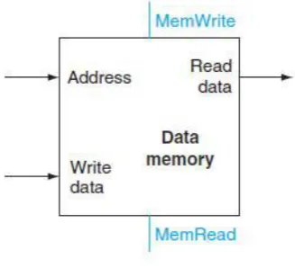
Data Memory:This is the second memory of the MIPS. This memory can be used for both Read and Write applications. Hence this circuit can be replaced by a Random Access Memory. The input is the address and if read signal is enable it reads the data from the inputs memory location. If write signal is enable it writes the data into the input's memory location.
FIG 2 DATA MEMORY
III.PROPOSED DESIGN
In exiting system there is no cell checking operation so it may not verifying the memory location twice. There is single memory cell array to send the data in single phase. There are the two problems in existing system, to overcome these problem we are proposing a new architecture.
The proposed system consisting of refresh control, flash timing controller, column address buffer, row address buffer, column decoder, row decoder, memory array, cell checking, data in/data out.
The refresh controller and flash controller will refresh all the data in memory array location. The row address buffer and column address buffer will send the buffer of address it may column or row. The address buffer is taken by their respective decoder, means column address buffer is given to column decoder and the buffer of address is decoded. Similarly row address buffer is given to row decoder to decode the buffer of address.
The output of row decoder and column decoder will select the memory location in memory array. As per the changing of row or column address buffer the decoder will change the memory location. The total memory location will call it as memory array.
The cell checking block will check either to select the memory location array i.e. S=0 or 1. If S=0 the memory location array one will select, and the data is impend in that array memory location. Else S=1 the second array memory location will select and the data impend in second memory array location.
The date-in used to write the data and data-out is used to read the data memory array. By using this proposed system we overcome checking the memory array and to array of two memory locations.
IV.RESULTS
The below figure 4 shows the RTL Schematic of proposed system
The developed proposed system with technology schematic is shown in below figure 5.
The total output is shown in below figure 6 as per the address of column and row the data is stored in that respective memory location
V.CONCLUSION
As there is a large number of possible failure modes for memories of flash, algorithms of long test that is automatic test equipment (ATE) which is complicated are commonly seen. Production row and column address bit cell as basis to probe for any possible weaknesses of the process or design in SRAM. There may be occurrence of sa0 and sa1 faults in any chip design, these faults are overcome by using row and column address cells we make perfect location to store the data and no cross sections of SRAMS. By extending of cell checking for memory array gives verification of memory location. The column address buffer and row address buffer are used to pick the memory location. By comparing with previous method the above two modules gives accurate selection of memory location of cell checking operation.
VI.REFERENCES
[1] Ting-Jung Lin, Wei Zhang, and Niraj K. Jha, ―SRAM-Based NATURE: A Dynamically Reconfigurable FPGA Based on 10T Low- Power SRAMs‖ IEEE Trans. VLSI Systems, accepted for future inclusion in IEEE journal.
[2] I. Kuon and J. Rose, ―Measuring the gap between FPGAs and ASICs,‖ IEEE Trans. Comput.-Aided Design Integr. Circuits Syst., vol. 26, no. 2, pp. 203–215, Feb. 2007.
Fig 4 RTL Schematic
Fig 5 Technology Schematic
[3] W. Zhang, N. K. Jha, and L. Shang, ―A hybrid nano/CMOS dynamically reconfigurable system—Part I: Architecture,‖ ACM J. Emerg. Technol. Comput. Syst., vol. 5, no. 4, pp. 16.1– 16.30, Nov. 2009.
[4] A. DeHon, ―Dynamically programmable gate arrays: A step toward increased computational density,‖ in Proc.
Canadian Wkshp. Field- Program.
Devices, 1996, pp. 47–54.
[5] H. Noguchi, Y. Iguchi, H. Fujiwara, Y. Morita, K. Nii, H. Kawaguchi, and M. Yoshimoto, ―A 10T non-precharge two-port SRAM for 74% power reduction in video processing,‖ in Proc. IEEE Comput. Soc. Annu. Symp. VLSI, 2007, pp. 107– 112.
[6] Md. A. Khan, N. Miyamoto, R. Pantonial, K. Kotani, S. Sugawa, and T. Ohmi, ―Improving multi-context execution speed on DRFPGAs,‖ in Proc. IEEE Asian Solid-State Circuits Conf., 2006, pp. 275– 278.
[7] S. Trimberger, D. Carberry, A. Johnson, and J. Wong, ―A time multiplexed FPGA,‖ in Proc. IEEE Symp. FPGAs for Custom Comput. Mach., 1997, pp. 22–28.
[8] T. Fujii, K.-I. Furuta, M. Motomura, M. Nomura, M. Mizuno, K.-I. Anjo, K.Wakabayashi, Y. Hirota, Y.-E. Nakazawa, H. Ito, and M. Yamashina, ―A dynamically reconfigurable logic engine with amulticontext/ multi-mode unified-cell architecture,‖ in Proc. IEEE Int. Solid- State Circuits Conf., 1999, pp. 364–365. [9] Sapna Singh, Neha Arora, MeenakshiSuthar and Neha Gupta (2012)―Performance Evaluation Of Different Sram Cell Structures At Different Technologies‖, Proc. of International Journal of VLSI design & Communication Systems (VLSICS) Vol.3. [10] W. Zhang, L. Shang, and N. K. Jha, ―A hybrid nano/CMOS dynamically reconfigurable system—Part II: Design optimization flow,‖ ACM J. Emerg. Technol. Comput. Syst., vol. 5, no. 3, pp. 13.1–13.31, Aug. 2009.
[11] G. Lemieux and D. Lewis, ―Circuit design of routing switches,‖ in Proc. Int. Symp. FPGA, 2002, pp. 19–28.
[12] Dr.Sanjay Sharma and ShyamAkashe (2011),―High Density Four- Transistor SRAM Cell With Low Power Consumption”, Proc. of Int. J. Comp.