as in digital electronics, VLSI (very large scale integration technology), DSP (digital signal processing), micro processors etc. In digital electronics adder is a digital circuit that is used to carry out addition of two numbers. In processor adder is the fundamental unit use to calculate the address, table indices. In VLSI it acts as the basic building block. In digital signal processing it is used in FIR, IIR filter. Today designing an adder is not an issue main prominence is on designing an adder having less delay, reduced chip area and consumes less power. In this paper 64-bit CLA is discussed and simulation results for 32bit and 64bit CLA has been exposed. The purposed design shows the Performance parameter chip area and delay in results. This adder is implemented using VHDL. Keywords- VLSI, CLA, VHDL, DE, DSP.
1. INTRODUCTION
Adders are most commonly used in various electronic applications. This is the basic building block of a unit. Different types of adders are available such as ripple carry; carry look ahead, carry select, carry save and many more. Each one having their own benefits and limitations. But the main issue is to design an adder having less delay, low power consumption and reduced chip area. In past, the major challenge for VLSI designer was to reduce chip area by using efficient optimization techniques. [1] Then the next phase is to increase the speed of operation to achieve fast calculations as, in today’s microprocessors millions of instructions are executed per second. Speed of operation is one of the major constraints in designing DSP processors. Now, as most of commercial electronic products are portable like mobile, laptops etc. These require more battery backup. So, lot of research is going on to reduce power consumption. Thus, there are three performance parameters on which a VLSI designer has to optimize their design i.e. area, speed and power. It is very difficult to achieve all constraints for particular design, therefore depending on demand or application some compromise between constraints has to be made. There are basically two types of adders a) Half adder b) Full adder. These are the main two adders from which others adders are derived .Half adder is used for addition of two numbers. Full adder is used for addition of three numbers in which A, B are two numbers and Ci is input carry. These three numbers are used as inputs and sum and carry out are the outputs.
Look ahead Carry Adder (CLA): CLA is derived from ripple carry adder. In ripple carry adder data flow in a chain as the bit length go on increasing delay increased to overcome that problem carry look ahead adder was designed. Look ahead carry algorithm speed up the operation to perform addition, because in this algorithm
input signals.
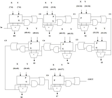
Carry look ahead logic uses the concepts of generating and propagating carries. Although in the context of a carry look ahead adder, it is most natural to think of generating and propagating of binary addition, the concepts can be used more generally than this. There will be a carry propagation if OR operation is performed for that either one of the input is one or input carry also be 1.For carry generation there should be AND operation for that both the inputs should be 1.Figure 1 represent the 64 bit carry look ahead adder which consist of 8 adders each one used for eight bit addition.
Generation and propagation can be represented by the Boolean expression in the following way:
Pi = xi or yi --- Carry Propagation Gi = xi and yi --- Carry Generate Ci+1 = Gi or (Pi and Ci)--Next Carry
Figure 1 shows 64-bit carry look ahead adder that consists of eight adders each one performing 8 bit addition.
II RELATED RESEARCH WORK
Various researches have been carried out in order to design adders and a few of them has been discussed here Hasan Krad proposed design of 32 bit multiplier using carry look ahead and carry select adder.Jing Fu Li suggested carry look ahead adder . Carry Look ahead Adder (CLA) is one of the fastest adder structures that is widely used in the processing circuits.
III METHODOLOGY
Adders are the basic unit to perform arithmetic and logic operation. Different types of adders has been designed each having its own benefits and limitations.
To Design the adders based on FPGA, procedure is: 1. To study the adder with their benefits and limitations. 2. After making comparison write vhdl code.
3. Implementation and Synthesize on the Xilinx ISE Design Suit 14.3, ISim simulator.
4. After syntesization observe the simulation results. Software to be used:
Digital Design Tools: 1. Xilinx ISE Design Suit 14.3 , ISim simulator ,
Figure1: Carry Look Ahead Adder
IV SIMULATION RESULTS
Simulation results show the final output. It also represents the RTL View, technology view for 32 bit carry look ahead adder.
4.1 RTL View: RTL is register transfer level. It describes the route through which the data transfer take place. It captures the behavior and converts it into circuit.
4.3 RTL view: RTL view for 64 bit carry look ahead adder is shown below.X, Y and carry_in are the inputs, sum and carryout are the outputs.
Figure: 3 RTL View for 64bit CLA 4.4 Technology view describes the technology used for the purposed work .It consist of n number of look up tables. Each look up table consists of Boolean expressions, logic circuit and K map. As the bit size increases it becomes complicated and number of look up tables get increased.
Figure:4 Technology view for 64 bit CLA
4.5 Simulation results for 64 Bit CLA:
Table1: Device Utilization Summary
Logic Utilization Used Available Utilization
No. of slices No. of 4 I\P LUT No. of bonded IOB
64 129 195 4656 9312 190 1% 1% 102%
This table represents the chip area consumed for the designing of 64bit carry look ahead adder. It shows the number of look up tables, input output and slices used out of total available data. This table also tells number of gates used for designing the adder. From this table it is cleared that utilization of number of input and output is high in comparison with the other components. Whereas number of slices and look up tables have almost same proportion.
4.6 Comparison between delay and memory:
This line graph describes the data of memory and delay. Delay is denoted in nanoseconds where as memory unit is Kilobytes (KB).Because delay is given in nanosecond which is very small in comparison with memory so it is marked at 0.
V CONCLUSION
Simulation results for 32bit and 64 bit carrylook ahead adder has been shown.Results of performance parameter delay and chip area has been revealed.
REFERENCES
[1] Hasan Krad and AwsYousif Al-Taie, “Performance Analysis of a
Bit Multiplier with a Carry-Look-Ahead Adder and a 32-bitMultiplier with a Ripple Adder using VHDL”, Journal of Computer Science 4 (4): 305-308, 2008 Asadi, P. and K. Navi “A novel high-speed 54-54-bit multiplier”,.
[2] H. Ling, “High speed binary adder,” IBMJ. Res. Develop., vol.
25, no. 3, pp. 156-166, May 1981.
[3] H. C. Lai, "A study of current logic design problems," Ph.D.
dissertation, Dep. Computer Sci., Univ. of Illinois, Jan. 1976.
[4] Jin-Fu Li, Jiunn-Der Yu, Yu-Jen Huang, “A Design Methodology
for Hybrid Carry-Lookahead/Carry-Select Adders with Reconfigurability”, IEEE, 2005.
[5] J.Sklansky. ‘Conditional Sum Addition Logic’, IRE Trans. EC-9
No. 2, 1960.
[6] M. J. Flynn and S. F. Oberman, “Modern research in computer
arithmetic,” Class notes, Stanford Univ., Stanford, CA, autumn quarter, 1998–1999.
[7] N. Quach and M. J. Flynn, “High speed addition in CMOS,”
IEEE Trans. Compute., vol. 41, pp. 1612–1615, Dec. 1992.
[8] Pak K. Chan, “Delay Optimization of Carry-Skip Adders and
Block Carry-Lookahead Adders Using Multidimensional Dynamic Programming”, IEEE Transactions on Computers, vol. 41, No. 8, pp. 920-93, 1992 193.
[9] R.W. Doran: ‘Variants of an Improved Carry Look-Ahead
Adder’, IEEE Trans. On Computers, 37, pp. 1110-1113, 1988.