Source Predictive Process Design Kit for 15nm FinFET Devices. (Under the direction of Dr. W. Rhett Davis).
The semiconductor industry has seen an exponential growth curve since the advent of MOS transistors, as computing power have scaled continuously with transistor sizes. However, this scaling now faces major roadblocks beyond 22nm due to excessive leakage and short channel effects. This has encouraged research on a multi-gate transistor architecture, FinFET, as an alternative to continue on the exponential growth curve. This further necessitates introduction of FinFET device and supporting tools into university education through development of open source process development kits.
In this thesis, FinFET device architecture is first studied, and lithographic and process challenges involved in the fabrication of sub-20nm device structures are analyzed. In particular, double patterning lithography technique is presumed for critical dimensions and basic methodology for design of FinFET layouts and the layer stack for integrated circuit fabrication is developed to meet these requirements. Design rules which play a crucial role in ensuring the yield and reliability of a layout are developed for good layout density considering lithographic constraints and also graphically explained.
by Kirti Bhanushali
A thesis submitted to the Graduate Faculty of North Carolina State University
in partial fulfillment of the requirements for the degree of
Master of Science
Electrical Engineering
Raleigh, North Carolina 2014
APPROVED BY:
_______________________________ ______________________________ Dr. Mehmet Ozturk Dr. Paul Franzon
________________________________ Dr. W. Rhett Davis
DEDICATION
BIOGRAPHY
ACKNOWLEDGMENTS
I would like to thank Dr. W. Rhett Davis for giving me an opportunity to work on this project and his assistance throughout this project. Our weekly meeting were a great learning experience, each time I learnt something new.
I would like to express deep gratitude to Alexandre Toniolo at NanGate Inc., as this project would not been possible without his support in development of design rules and explanation of Local interconnect layers was crucial to this project.
I am also extremely grateful to the team at Mentor Graphics, particularly Tarek Ramadan, Ahmed Hammed Fathy, Omar El-Sewefy, Ahmed El-Kordy, and Hend Wagieh for developing the first cut of the design rules and also supporting us throughout this project.
I would like to thank my family and friends back home in India for their patience and for encouraging me throughout these years.
TABLE OF CONTENTS
LIST OF TABLES ...vii
LIST OF FIGURES ... viii
1 INTRODUCTION... 1
1.1 Motivation... 1
1.2 Thesis Outline ... 2
2 SEMICONDUCTOR TECHNOLOGY BEYOND 22NM ... 4
2.1 Issues with bulk technology... 5
2.1.1 Leakage power consumption ... 5
2.1.2 Random Dopant Fluctuation ... 8
2.1.3 Channel Length modulation... 10
2.1.4 Drain Induced Barrier Lowering (DIBL) ... 11
2.1.5 Gate Induced Drain Leakage (GIDL) ... 12
2.2 Introduction - FinFET ... 13
2.3 Operation of FinFET ... 16
2.4 FinFET Performance ... 18
2.4.1 Advantages ... 18
2.4.2 Issues ... 22
3 INTRODUCTION TO FINFET FABRICATION PROCESS AND LAYERS ... 25
3.1 FinFET fabrication – 15nm ... 25
3.2 Lithography Techniques ... 25
3.2.1 Double patterning Lithography (DPL) ... 26
3.3 Introduction to FreePDK15™ layers ... 28
3.3.1 Back-End-Of-Line (BEOL) Layers ... 28
3.3.2 Cut Layer ... 30
3.3.3 Middle-of-line Layers (MOL)... 31
4 DEVELOPMENT OF DESIGN RULES FOR FREEPDK15™ ... 34
4.3 DRC software... 34
4.2.1 Width Rules ... 35
4.2.2 Spacing Rules ... 36
4.2.3 Enclosure Rules ... 36
4.2.4 Overlap Rules ... 37
4.2.5 Area Rules ... 38
4.2.6 Antenna Rules ... 38
4.2.7 Multi-colored design rules ... 38
4.2.8 Restrictive Design Rules (RDR) ... 39
4.3 Design Rules for FreePDK15™ ... 40
4.3.1 NWell (NW) Rules ... 40
4.3.2 Active (ACT) Rules ... 42
4.3.3 GATE design rules ... 46
4.3.4 GATEAB rules... 49
4.3.5 Gate cut mask (GATEC) rules ... 51
4.3.6 Threshold voltage adjust layer (VTH/VTL) rules ... 54
4.3.7 NIM/PIM rules ... 56
4.3.8 Active Interconnect Layer-1 (AIL1) rules ... 59
4.3.9 Active Interconnect Layer-2 (AIL2) rules ... 61
4.3.10 Gate Interconnect layer (GIL) rule ... 64
4.3.11 Via0 Rule (V0) rule ... 67
4.3.12 Metal1 Rules ... 71
5 FINFET LAYOUTS AND DESIGN RULE VALIDATION ... 82
5.1 Single Transistor Layout of a FinFET ... 82
5.2 Design rule validation ... 84
5.2.1 Minimum size inverter cell: ... 84
5.2.2 NAND4 cell ... 85
5.2.3 Tiled Inverter and NAND4 cells ... 86
5.2.4 Layout Density Comparison ... 88
6 CONCLUSION AND FUTURE WORK ... 91
LIST OF TABLES
Table.4.1: NWell design rules………..41
Table 4.2: Active design rules………...43
Table 4.3: GATE layer design rules………..46
Table 4.4: GATEAB layer design rules….……….…...49
Table 4.5: GATEC layer design rules………...51
Table 4.6: VTH/VTL layer design rules……….………..54
Table 4.7: NIM/PIM design rules……….56
Table 4.8: AIL1 design rules………59
Table 4.9: AIL2 design rules………61
Table 4.10: GIL design rules………64
Table 4.11: V0 design rules...67
Table 4.12: M1A design rules………...71
LIST OF FIGURES
Fig. 2.14: Leakage path away from the MOSFET………..…..19
Fig. 2.15: A lower Sub-threshold slope can be leveraged to operate the device at lower power and/or to improve speed performance………...19
Fig. 2.16: Plot of GDS vs Physical length for FinFET and Planar devices………....20
Fig. 2.17: Comparison of sigma (VTH ) for FinFET and planar FET………...21
Fig. 2.18: Width Quantization………...………...22
Fig. 2.19: Detail list of FinFET capacitances………...………...……..…23
Fig. 3.1: Representation of Double Patterning using two colored mask. (a) Metal Pitch – Metal1A is ‘X’ (b) Metal Pitch – Metal1B is ‘X’ (c) Final Metal pitch is ‘X/2’………..……..27
Fig. 3.2: Steps involved in Self-Aligned-Double-Patterning Lithography……...………....…28
Fig. 3.3: Representation of cross-section of hierarchical metal layer scaling…………..…..…29
Fig. 3.4: Typical digitized 6bit SRAM cell and its expected printed image on Silicon…...…30
Fig. 3.5: Shows resulting printed in double patterning image due to horizontal and vertical mask misalignment. Horizontal misalignment results in reduced gate length ‘Lg’ and vertical misalignment results in reduced device Width ‘W’………..30
Fig. 3.6: Shows how printing the contiguous gate layer and then using the cut mask to remove the unwanted part of the gate helps in achieving the best printout for devices………..31
Fig. 3.7: Cross-section of FinFET………..………..32
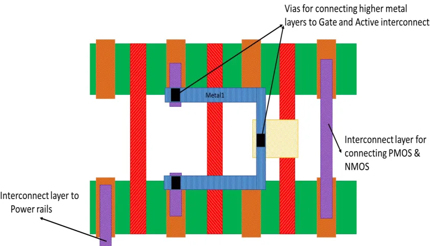
Fig. 3.8: Shows use of local interconnect layers for connecting the internal nets and for connection to the power rails………....33
Fig. 4.2: Via misalignment………...………...……….37
Fig. 4.3: Minimum overlap of the two shapes………...………...……….37
Fig. 4.4: Pitch Rule between metal layers…………...…...………...……39
Fig. 4.5: Pinching seen in the case of jogs. As shown, pinching can be removed by using thicker layer at the bend…….………...40
Fig. 4.6: Graphical explanation of NW rules………...…………...………..42
Fig. 4.7: Graphical representation of ACT rules…………...…………...……….45
Fig. 4.8: ACT.2 rule………...………...46
Fig. 4.9: Graphical representation of GATE layer rules………...……….49
Fig. 4.10: Graphical representation of GATEAB layer rules………...51
Fig. 4.11: Graphical representation of GATEC layer rules………...………54
Fig. 4.12: Graphical representation of VTH/VTL layer rules………...………56
Fig. 4.13: Graphical representation of NIM/PIM layer rules………...……….58
Fig. 4.14: Graphical representation of AIL1 rules………...……….61
Fig. 4.15: Graphical representation of AIL2 rules………63
Fig. 4.16: Graphical representation of GIL rules………...………...67
Fig. 4.17: Graphical representation of V0 rules………...……….71
Fig. 4.18: V0 spacing rules………...72
Fig. 4.19: Graphical representation Metal1 design rules………...………79
Fig. 5.1: Basic transistor Layouts of (a) Planar MOS device (b) a FinFET and(c) a FinFET as
seen on the physical mask……….83
Fig. 5.2: Dummy Gates for Uniformity in FinFET………...………83
Fig. 5.3: Inverter cell for 15nm FinFET device……...………..84
Fig. 5.4: NAND4 standard cell for 15nm FinFET…………...………..86
Fig. 5.5: Tiled Inverter cells for 15nm FinFET…………...………..87
Fig. 5.6: Tiled NAND4 cells for 15nm FinFET……...……….88
1
INTRODUCTIONThis chapter discusses the motivation behind development of an Open Source Process design kit FreePDK15™ for 15 nm FinFET devices. In the latter part of the chapter a brief outline of the thesis is presented.
1.1Motivation
International Technology roadmap for Semiconductors (ITRS) [1] predicts physical length of transistors to scale down to 16 nm by 2016. However, bulk CMOS technology suffers from high leakage power, random dopant fluctuations and other short channel effects which greatly limit the scaling of the bulk CMOS technology beyond 22nm feature size. Thus, the current trend in semiconductor technology is in the direction of development Fully Depleted Silicon On Insulator (FDSOI) and multi-gate FinFET architectures, as they offer lower leakage power and improved short channel characteristics. A literature survey of the ION against IOFF performance [6] [7] [8] [9] of FinFET and FDSOI devices at 22nm indicates that FinFET have a higher drive current for the same IOFF. In addition, due to the wrapping nature of the gate structure in FinFET they have low leakage power and better short channel characteristics.
Foundries like Intel and TSMC are expected to roll out FinFET at 15nm and 16nm feature size respectively in couple of years [2].
It can be seen that FinFET devices are to dominate the silicon roadmap for the foreseeable future. Thus, it is necessary to introduce this technology in university education and research for the designers to gain an understanding. It is necessary to develop Process Development Kits (PDK) in order to understand the complexity of these new processes [5]. However, intellectual property is strictly held on to by the industry and it requires large investment for licensing this technology which is beyond the scope of universities and educational institutions. As training the next generation of VLSI designers is of paramount importance it is necessary to develop these tools and process development kits.
This provides the motivation for development of open source tools and a PDK which can support sub-20nm FinFET technology. Additionally, Schuddinck et. al, [35] shows examples of 15nm FinFET standard cells and these layouts are used as a reference for FreePDK15 which offers a physical gate length of 15nm, 16nm and 20nm. This project is thus a step towards development of an open source PDK. As part of this project, FinFET architecture is analyzed Additionally, a set of design rules meeting the requirements of double patterning lithography are developed and a Calibre Design rule deck file is created and evaluated on a set of standard cell layouts.
1.2Thesis Outline
2 SEMICONDUCTOR TECHNOLOGY BEYOND 22NM
Since the advent of MOSFET technology, bulk MOSFETs have been the preferred choice of the semiconductor industry due to their simplified planar fabrication process. A bulk MOSFET is a planar four-terminal transistor and consists of a single gate structure that controls the channel current. The device is shown in Fig. 2.1 and its four terminals are the Gate, the Drain, the Source and the Bulk, with the Gate terminal isolated from the bulk by an oxide layer. A MOSFET works on the basic principle of formation of an inversion charge layer by application of potential difference between the Gate and the Bulk terminal and thus the name Field Effect transistor (FET). This charge layer starts conducting on application of a potential difference between the Drain and the Source terminal.
As MOS technology has scaled several techniques have been adopted to improve performance. The major changes to the original structure include use of Metal Gate High-K stack to overcome the issue of Random Dopant Fluctuation (RDF) and gate leakage. However, bulk technology has now reached its limit and suffers from several issues when scaled beyond 22nm.
This section presents some of these problems and introduces FinFET as a prospect beyond 22nm. The multi-gate architecture of the device is explained and further, the current flow in the channel is described. The chapter ends with an overview of the advantages and challenges seen with adoption of multi-gate architecture.
2.1Issues with bulk technology
As a direct consequence of scaling, short channel length devices exhibit a number of second order effects which are not generally observed in longer channel devices. Some of these effects, like channel length modulation, drain induced barrier lowering (DIBL), Gate induced drain leakage (GIDL) and sub-threshold conduction deteriorate MOSFET performance. In order to overcome these effects, body doping is increased, but it results in random variation of the threshold voltage. This section describes these second order effects in detail.
2.1.1 Leakage power consumption
Total power dissipation in CMOS is described by the following equation: 𝑃𝑎𝑣𝑔 = 𝑃𝑠ℎ𝑜𝑟𝑡+ 𝑃𝑑𝑦𝑛𝑎𝑚𝑖𝑐+ 𝑃𝑙𝑒𝑎𝑘𝑎𝑔𝑒 (2.1)
where Pshort represents the power dissipation due to direct short circuit path current Isc which happens when both PMOS and NMOS are conducting. Dynamic Power Pdynamic represents the power dissipation due to the charging and discharging of load capacitor CL. Leakage Power Pleakage is the power dissipation because of the leakage current Ileak in the off-state. For deep
submicron (DSM) devices, leakage power due to increase in Ileak is one of the major contributors to average power dissipation. In MOSFETs, the main mechanism behind power leakage is flow of sub-threshold leakage current or off-state leakage current.
2.1.1.1 Sub-threshold Leakage
The transition of a MOSFET from the OFF-state to the ON-state is not as abrupt as is modeled by its piece-wise linear model shown in Fig.2.2.
VGATE
IDRA
IN
VTH
In the sub-threshold or OFF-state region, the potential across the channel is almost constant and drift current is negligible. In practice, however, a channel current exists and it is essentially caused by the diffusion of minority carriers due to a concentration gradient between the drain/source and the body. This leakage current varies exponentially with gate voltage [10].
The sub-threshold swing S of a MOSFET is defined by the following equation
Ioff = IVT 10-Vt/S (2.4)
where IVT is the current at which threshold voltage VT is defined. The equation and the ID vs VGS characteristics in Fig.2.3 indicate that the leakage current largely depends on IOFF,
threshold voltage VT and the sub-threshold slope. A lower sub-threshold slope is desired for low power operation. As shown by Cho et.al [13] the sub-threshold slope has degraded with scaling and is around 90dB/dec for 20 nm Bulk MOSFET. As a result, the contribution of Sub-threshold leakage to the total power dissipation has significantly increased and is a major impediment to circuit design.
2.1.2 Random Dopant Fluctuation
As the planar MOSFET transistor scales beyond 20 nm gate length, the impact of channel doping on the characteristic of MOSFET becomes more dominant [14]. The discrete dopant distribution is random and this results in random threshold voltage fluctuations and drive current mismatch [14]. Figures 2.4, 2.5 and 2.6 present the distribution of ION, IOFF and saturation threshold voltage VTS with channel dopants. Saturation threshold voltage is defined as the gate voltage for which saturation drain current is 100 nA.
Fig. 2.5 Distribution of IOFF with Channel dopants for 20 nm transistors [14]. This shows that IOFF varies by up to 20% with variation in channel dopant concentration.
Fig. 2.6 Distribution of VTS with Channel dopants for 20 nm transistors [14]. This shows that the threshold voltage varies by up to 200 mV with channel dopant concentration
2.1.3 Channel Length modulation
The long channel current equation for a MOSFET suggests that the channel current is constant in saturation region.
𝐼𝑑𝑠𝑎𝑡 =𝛽(𝑉𝑔𝑠− 𝑉𝑡)2 2 ; Vds > Vgs –Vt (2.6)
As the channel length decreases, it is seen that the channel current begins to depend on drain voltage. This happens as the depletion width near the drain increases because of the presence of extra dopants. Thus, the effective channel length decreases and the equation for the drain current ID is modified as follows
ID = Idsat (1 + λVDS ) (2.7)
Fig. 2.7 ID vs VDS plot for an NMOS
2.1.4 Drain Induced Barrier Lowering (DIBL)
Drain Induced Barrier lowering is a short channel phenomenon in which the drain voltage starts controlling the threshold voltage of the device. DIBL is measured by change in threshold voltage VT due to drain bias VDS (ΔVT / ΔVDS ) and becomes more prominent for higher drain voltages. At the drain, DIBL causes the channel current to increase as the voltage starts controlling the inversion layer charge. The impact of DIBL has increased with scaling and as reported by Cho et.al [13] is ~ 100mV/V for 20 nm Bulk MOSFETs.
Dr
a
in
c
ur
re
n
t
ID
Drain to source voltage VDS
Fig. 2.8 ID and Gate voltage VG plot for two drain voltages. When the drain current is high, electrical characteristics are left-shifted due to DIBL [17].
2.1.5 Gate Induced Drain Leakage (GIDL)
overlapped region. A significant drain leakage current is seen in this condition and is plotted in Fig. 2.9.
Fig. 2.9 GIDL current in medium VT, Low VT and High VT 45 nm NMOS transistor [18]
2.2 Introduction - FinFET
Fig. 2.10 Cross-section of Intel’s Tri-gate [19]
Fig. 2.11 3D view of Intel’s Tri-gate device [19] Hfin
In a FinFET, a thin slice of Silicon called as “fin” is wrapped on three sides by a gate, and this is how the FinFET derives its name. This wrapping allows the gate to exercise greater electrical control over the channel and helps in reducing short channel effects and leakage current. The current flows along the top surface of the Fin, as shown in in Fig. 2.11.
Due to the three-dimensional nature of a FinFET structure it is possible to pack more number of transistors in the same area. Also, this structure increases the effective width Weff of the device as given by
Weff = 2HFin + WFin (2.7)
where HFin is the height of the fin and WFin is the width of the Fin. These factors aid in attaining higher ION per unit area.
The fin is a fully depleted thin slice of Silicon. This eliminates the need for implanting dopant atoms, which would otherwise contribute to RDF. It also helps in overcoming short channel effects as well as in eliminating the leakage path away from the gate.
The fin width has to be less than the gate length to have greater electrical control over the channel. It is seen that devices with fin widths half that of the fin length have a better leakage performance [13]. Thus the Width of the fin and the Length have to scaled together in order to harness the advantage of fins.
2.3 Operation of FinFET
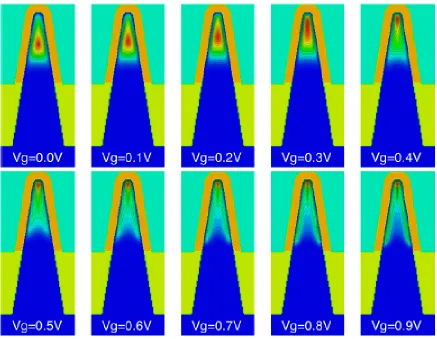
Basic principle behind the operation of FinFET is through control of channel charge by a three-dimensional gate, which is basically the same as that of a planar MOSFET. They have three regions of operation and the ID –VDS and the ID-VDS curves for a 25nm FinFET are as shown in Fig. 2.12.
Fig. 2.12 ID-VDS curves for a 25nm FinFET [12]
minimum in the middle of the channel and this results in off state leakage current. At higher gate voltages the current density distribution is maximum at the Fin-oxide interface. Due to this non-uniform nature of the current density distribution for different gate biases, the compact model are much more complicated than planar MOSFET.
2.4 FinFET Performance
The FinFET structure and its characteristics have been discussed in the previous sections and they have a considerable impact on the performance of the circuit. In the following section, the performance advantages of this device in terms of speed and power are evaluated and the challenges incurred during device circuit co-design are discussed.
2.4.1 Advantages
FinFET structure are anticipated to have multiple benefits like low power operation, reduced short channel effects and improved performance. The following section analyses these features and compares these performance metrics with bulk MOSFET.
2.1.4.1Reduction in Leakage power:
One way is to keep the same ION and achieve a lower leakage current IOFF. The second method is to increase ION and achieve lower threshold voltage for the same leakage current for improving the speed performance as shown in Fig. 2.15.
Multi-gate transistors also exhibit a lower DIBL effect by eliminating the influence of drain potential on the channel in OFF state.
Fig. 2.15 A lower Sub-threshold slope can be leveraged to operate the device at lower power and/or to improve speed performance [19]
GATE
SOURCE DRAIN
Leakage Path
2.4.1.2Higher output impedance and thus better analog performance
Channel Length modulation is predominantly seen due to the shortening of the channel length beyond the pinch off point. Because of the wrapping of the gate around the fin and the narrow width of the Fin, it is fully depleted. Therefore, increase in drain voltage doesn’t deplete the fin further and the variation in channel length is low. The reduced variation in channel current with respect to drain voltage results in a lower output trans-conductance GDS = ID / VDS. Lower output trans-conductance translates into higher output impedance and thus a higher intrinsic gain Av = Gm* r0.
Fig. 2.16 Plot of GDS vs Physical length for FinFET and Planar devices [15]
2.4.1.3Lower Random Dopant Fluctuation (RDF)
RDF induced threshold voltage variation can be reduced by using light channel surface doping or fully depleted thin-body, as FinFETs use an undoped body they are immune to RDF except for the variations introduced by impurities in the body. A relative study of threshold variation sigma (VTH) for FinFET and MOSFET shown in Fig. 2.17 indicates a substantial decrease in sigma (VTH) due to both body and source/drain RDF.
Fig. 2.17 Comparison of sigma (VTH ) for FinFET and planar FET [23]
2.4.1.4Higher drive current
2.4.2 Issues
Multi-gate technology introduces additional challenges during the design cycle which complicate the device circuit co-design. A new design approach is required to accommodate thermal characteristics and device sizing, these issues are illustrated in the following section.
2.4.2.1Width quantization
The total width of a FinFET is an integer multiple of individual fin width. The width of the device is one of the main design variable for modifying transistor characteristics however, device width can only increase in discrete steps for FinFET as shown in Fig. 2.18 for a 3 fin structure. Standard cell design requires complex device sizing in order to achieve a balance between power and speed, however, the discrete nature of the FinFET width limits this option.
Fig. 2.18 Width Quantization [19] Hfin
Wfin Total_width = N*Weff
2.4.2.2Higher intrinsic capacitances
Due to the wrap around nature of the gate, the FinFET structure tends to have higher parasitic capacitances. A complex parasitic model of a FinFET is shown in Fig. 2.19. The introduction of these parasitic capacitance complicate the layout extraction model of a FinFET and also limit their speed performance.
Fig. 2.19 Detail list of FinFET capacitances [26]
2.4.2.3Complex Thermal Characteristics
3 INTRODUCTION TO FINFET FABRICATION PROCESS AND LAYERS
Integrated circuit fabrication using FinFET technology for 15nm technology nodes involves a lot of technical challenges including limitation of the optical lithography process and introduction of specific interconnect layers. This chapter presents double patterning lithography process and explains the additional constraints introduced due to double patterning lithography. The chapter ends with a discussion on the layer stack used for FreePDK15™. 3.1 FinFET fabrication – 15nm
FreePDK15TM kit is a 15nm FinFET technology kit, the selection of 15nm was done on the basis of ITRS-2011 table, which predicts a physical length of 16nm by 2016. However, the definition of 15nm FinFET technology is ambiguous as Schuddinck et.al, [35] which is a representative of industry, shows a standard inverter and NAND4 cell layouts and uses a physical length of 19nm for a 14nm FinFET technology. FreePDK15 thus provides an option of 16nm and 20nm for physical lengths.
3.2 Lithography Techniques
which uses single exposure technique with sub 20 nm laser wavelength. EUV could thus be the next big step in fabrication technology, but its viability in volume production is currently held up by insufficient wafer throughput. Additionally, use of EUV technology would require a complete over-haul of current photo-lithography tools.
As a result major foundries have extended the use of photo-lithography by use of innovative solutions like Double Patterning. In this section, the process of double patterning is presented.
3.2.1 Double patterning Lithography (DPL)
Double patterning lithography is a lithography technique adopted for integrated circuit fabrication beyond 32nm and aims to double pitch density to twice the pitch density achieved by single patterning technique. In order to achieve a higher layout density a layout is decomposed into two different masks with two different colors. Figure 3.1 shows a representation of double patterning for a metal layer, it illustrates how using two different colored masks for metal layers can help achieve a twice the pitch density.
(a) (b)
(c)
Fig. 3.1 Representation of Double Patterning using two colored mask. (a) Metal Pitch – Metal1A is ‘X’ (b) Metal Pitch – Metal1B is ‘X’ (c) Final Metal pitch is ‘X/2’
3.2.1.1 Self-Aligned Double Patterning Lithography (SADP)
followed by another etching process to remove the resist pattern and the hard mask. Lastly, the residual spacers are removed which leaves behind thinner denser final pattern.
Fig. 3.2 Steps involved in Self-Aligned-Double-Patterning Lithography [31]
3.3 Introduction to FreePDK15™ layers
This section introduces the Metal layer stack used for FreePDK15™. Additionally, the FreePDK15™ provides additional layers like cut mask and local interconnect layers which are discussed here.
3.3.1 Back-End-Of-Line (BEOL) Layers The metal layer stack can be divided into
2. Intermediate metal – It is an interface layer between metal layer and semi global metal layer and generally used for routing between two devices.
3. Semi-global metal – It is wider metal layer (twice the metal1 width) and is generally used for connection between different circuits.
4. Global Metal layers - It is the widest metal layer (four times metal1 width) and it is used for routing global nets like power and clock.
The layer stack follows a typical hierarchical scaling of ASIC architecture [30] and the cross section of the representation of hierarchy scaling of these metal layers is as shown in Fig. 3.3.
3.3.2 Cut Layer
Cut mask/Cut layers are used by Self-aligned-double-patterning lithography as it becomes difficult to print non-uniform structures below 22 nm. The process starts with printing a wide area of uniform structure and then defining the required features by cut mask. The primary use of Cut mask is to remove the unwanted features that are printed by the previous mask. It can be seen how a cut mask is used while printing 6 bit SRAM cell in order to overcome misalignment [32] as shown in Figures 3.4 to 3.6.
Fig. 3.4 Typical digitized 6bit SRAM cell and its expected printed image on Silicon [32]
Fig. 3.6 Shows how printing contiguous gate layer and then using the cut mask to remove unwanted part of the gate helps in achieving the best printout for devices [32]
3.3.3 Middle-of-line Layers (MOL)
Fig. 3.7 Cross-section of FinFET
Explanation of local interconnect layers:
1. Active Interconnect Layer-1 (AIL-1): It is used for connecting the individual fins of the FinFET
2. Active Interconnect Layer-2 (AIL-2): It is used for connecting the AIL-1 layers and thus the fins to the B-E-O-L like Metal1 through a via.
4 DEVELOPMENT OF DESIGN RULES FOR FREEPDK15™
Design rules are a set of geometric and connectivity guidelines for constructing the process mask, and they are specific for a particular semiconductor technology and lithography process. They help the designer verify the mask design before sending it for fabrication and are thus an important interface between designers and process engineers. Also, semiconductor manufacturing suffers from process variability and this necessitates confirmation of the design against set design rules. This is achieved in Electronic Design Automation (EDA) tools by a process called Design Rule Check (DRC).
The main objective of DRC is to achieve high yield for the design, since if the design rules are violated the design may not function as desired. However, at the same time, design rules are a primary determinant of the layout density and thus the cost of the technology [36]. Thus, it is necessary to develop optimum design rules that meet the requirements of high layout density and high yield.
This chapter describes the types of design rules and the programming language used for their development. Additionally, all the design rules for FreePDK15™ are listed and explained.
4.3 DRC software
generation of the derived layer, electrical and geometric rule checking, connectivity extraction, circuit comparison, and parasitic extraction [40].
4.3 Types of design rules
Design rules can be categorized on the basis of different geometrical, electrical and lithographic constraints. Conventionally, a simple classification based on minimum width or minimum spacing of a feature was sufficient for designing functional layouts. However, the escalation of lithographic requirements has increased the complexity of design rules, thus necessitating the introduction of additional restrictive design rules.
This section describes basic design rule types used in the design rule deck of FreePDK15™.
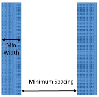
4.2.1 Width Rules
Fig. 4.1 Width and Spacing rules
4.2.2 Spacing Rules
The spacing between any two shapes is defined by the distance between the outside edges, and one of the most common form of spacing rules used is the minimum spacing rule (Fig.4.1). This rule ensures electrical isolation between two shapes, for example, two wells [11]. Failure to meet this rule may result in a short circuit. [34].
4.2.3 Enclosure Rules
Fig. 4.2 Via misalignment
4.2.4 Overlap Rules
The overlap rule is defined by calculating the distance between the internal edges of the overlapping shapes [34] (Fig. 4.3). The overlap rule is violated due to the misalignment between the two shapes and may result in an unwanted short circuit or an open circuit in the layout.
4.2.5 Area Rules
Typically, this rule is used to ensure that no shape in the design has an area less than the minimum defined area. It is generally defined so that the area of a shape is greater than the minimum area of the shape beneath it during processing [34].
4.2.6 Antenna Rules
In advanced processes, the wires are taller than they are wider, and thus plasma etching is generally used for fabrication of metal layers. The ionization process involved in plasma etching may impact the metal layer due to transfer of charge by ionized molecules. This charge can buildup on a net and exceed the breakdown voltage of the transistor gate. Thus, tunneling current density through the oxide must be kept below a certain threshold in order to satisfy the antenna rule. It can be seen from [36] that the tunnel current density depends on a simple ratio of metal area to transistor gate area, and these rules thus define a maximum ratio of metal area to transistor gate area.
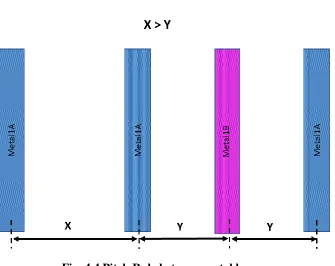
4.2.7 Multi-colored design rules
Fig. 4.4 Pitch Rule between metal layers
4.2.8 Restrictive Design Rules (RDR)
time, these rule cause an increase in the overall area of the layout, and thus are only used for critical dimensions.
Fig. 4.5 Pinching seen in the case of jogs. As shown, pinching can be removed by using thicker layer at the bend. [36]
4.3 Design Rules for FreePDK15™
Based on lithographic requirements, a set of design rules were developed for 15nm FinFET device process design kit FreePDK15™. This sections discusses these design rules for all the layers.
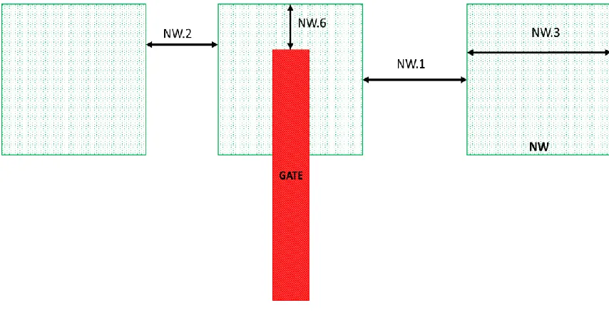
4.3.1 NWell (NW) Rules
Table.4.1 NWell design rules
Rule
#
Value Description Rationale
NW.1 180
nm
Minimum spacing of NW/(not NW)
at a different potential
Spacing rule to provide electrical
isolation and prevent punch-through
between separate wells [34].
NW.2 110
nm
Minimum spacing of NW/(not NW)
at the same potential
Spacing rule to provide electrical
isolation and prevent punch-through
between separate wells at same
potential [34].
NW.3 160
nm
Minimum width of NW/(not NW)
The width of 160nm required for a
single standard cell.
NW.4
0.140
um2
Minimum area/enclosed area of
NW
Minimum area sufficient for
constructing a single standard cell.
NW.5 NW must be orthogonal
Restriction rule added since
orthogonal structures simplify cell
Fig. 4.6 Graphical explanation of NW rules
4.3.2 Active (ACT) Rules
Table 4.2. Active design rules
Rule # Value Description Rationale
ACT.1 48
nm
Minimum vertical width of ACT
Schuddinck et al. [35] shows that
device with fin pitch of 40nm has
tolerable W-Si interface resistance
~80Ω. As fin Pitch is scaled from
45nm [35] to 40nm, fin width is also
scaled from 10nm [3] to 8nm. As
minimum vertical width of ACT is
2*Half_Fin_width + Fin_pitch,
minimum vertical width is calculated
as (2*4+40) nm = 48nm
ACT.2 40
nm Incremental vertical width of ACT
Device with fin Pitch of 40nm has a
tolerable W-Si interface resistance
and low epi-to-gate capacitance
Table 4.2. Continued
ACT.3 62
nm Minimum vertical spacing of ACT
Rule to provide electrical isolation
between two Active areas. Off-axis
illumination technique makes the
vertical spacing different from
horizontal spacing. Calculated to
ensure spacing greater than one
pitch spacing in ACT.
ACT.4 112
nm
Minimum horizontal width of ACT
Defined by minimum width required
for formation of a single transistor
with dummy gates.
ACT.5 80
nm Exact Horizontal spacing of ACT
Spacing to place exactly two
different dummy gates between
two active regions [38].
ACT.6 112
nm
Minimum notch of ACT
Same as minimum horizontal width
since notch is assumed to be
implemented using special
resolution technique, for e.g. cut
Table 4.2 Continued
ACT.7 31
nm
Minimum enclosure/spacing of
NW to ACT
Vertical spacing rule of ACT-ACT is
62nm, dividing that into two and also
to ensure extension of NW beyond
ACT.
ACT.8
0.005
um2
Minimum area/enclosed area of
ACT
Calculated for a two fin device
Fig. 4.8 ACT.2 rule
4.3.3 GATE design rules
The FreePDK15™ design kit assumes use of double patterning for GATE layers, and GATE layers GATEA and GATEB are the two different gate patterns used. This section explains the design rules for these GATE layers.
Table 4.3. GATE layer design rules
Rule # Value Description Rationale
GATE.1 20
nm
16
nm
GATE[A|B] exact horizontal
width
Gate length of 19nm in [35]
modified to values 20 nm, 16 nm
based on ITRS 2011 table [1]. Only
exact width values used for process
Table. 4.3. Continued
GATE.2
128
nm
Horizontal Pitch of GATE[A|B]
This value calculated to allow
minimum active region between the
two dummy gates [35].
GATE.3 44
nm
Min HORIZONTAL spacing of
GATEA and GATEB
Minimum horizontal spacing
calculated from minimum horizontal
pitch in [35].
GATE.4 GATE[A|B] may not bend
Gate bending causes pinching and
requires introduction of special
rules. These rules are currently not
part of FreePDK15™ [36].
GATE.5 38
nm
ACT min extension past
GATE[A|B]
Used to satisfy minimum horizontal
spacing rule between GATEA and
GATEB.
GATE.6 62
nm
GATE[A|B] min extension past
ACT
To ensures uniform transistor
formation in case of misalignment.
This rule is equal to vertical spacing
rule of ACT as off-axis illumination is
Table. 4.3. Continued
GATE.7
200
nm GATE[A|B] minimum length
Length is sufficient for at least one
transistor and minimum extension
on two sides of the ACT.
GATE.8
236
nm
GATE [A|B] maximum distance
to neighbor shape.
All the GATEA|B layers are printed
simultaneously and inessential
layers are removed using cut mask
layer GATEC. This rule ensures that
only one neighboring transistor can
be skipped and thus prevents
cutting out of two consecutive
Fig. 4.9 Graphical representation of GATE layer rules
4.3.4 GATEAB rules
The FreePDK15™ kit also provides a single colored gate layer called GATEAB with an assumption that the coloring of the gates would be done at process level. This section introduces the design rules for GATEAB layer and also gives a graphical explanation of each rule.
Table 4.4. GATEAB layer design rules
Table 4.4 Continued GATEAB.1 20 nm 16 nm
GATEAB exact horizontal
width
Same as GATE.1 rule with the
exception that GATE has a single
color. Coloring of these gate layers
implemented at process level.
GATEAB.2 64
nm
Horizontal Pitch of GATEAB
Pitch is half that of GATEA|B since
coloring is a post processing step.
GATEAB.3 44
nm
Min HORIZONTAL spacing of
GATEAB
Same as GATE.3
GATEAB.4 GATEAB may not bend Same as GATE.4
GATEAB.5 38
nm
ACT min extension past
GATEAB
Same as GATE.5
GATEAB.6 62
nm
GATEAB minimum extension
past ACT
Same as GATE.6
GATEAB.7 200
nm
GATEAB minimum length Same as GATE.7
GATEAB.8 236
nm
Maximum distance of GATEAB
to neighboring shape.
Fig. 4.10 Graphical representation of GATEAB layer rules
4.3.5 Gate cut mask (GATEC) rules
The FreePDK15™ kit provides a gate cut mask layer (GATEC) for removing unwanted printed features. This section introduces the design rules for GATEC layer.
Table 4.5. GATEC layer design rules
Table 4.5 Continued
GATEC.1.a 32
nm
Exact vertical width of GATEC
(shape is oriented
horizontally)
Cut layers vertical width selected to
be equal to the spacing between two
fins and the minimum spacing
between actives.
GATEC.1.b 64
nm
Exact horizontal width of
GATEC (shape is oriented
vertically)
Definition of a square cut drawn on a
gate.
GATEC.2.a 128
nm
Minimum horizontal length of
GATEC (shape is oriented
horizontally)
Assumption of 22nm min extension
of GATEC past GATEA|B and min
length for Resolution Enhancement
Technique that overlaps two
consecutive gates.
GATEC.2.a 64nm
Exact vertical length of GATEC
(shape is oriented vertically)
Definition of a square cut drawn on
a gate.
GATEC.3
128
nm
Minimum space of GATEC
Table 4.5 Continued
GATEC.4 22nm
Minimum extension of GATEC
past GATE[A|B] horizontally
To force GATEC alignment. This
value was calculated assuming
128nm length (horizontal direction),
cutting two gates only.
GATEC.5 15 nm GATEC minimum space to ACT
Spacing 62nm - GATEC width on
horizontal shape (32nm) = 30nm.
Divided it by two to define min
space to ACT.
GATEC.6 GATEC may not bend
Gate bending results in pinching and
requires introduction of special
rules. These rules are currently not
part of FreePDK15™ [36].
GATEC.7
GATEC shape bottom or top
must be aligned if distance <
192 nm
Used to add regularity in the layout
Fig. 4.11 Graphical representation of GATEC layer rules
4.3.6 Threshold voltage adjust layer (VTH/VTL) rules
The FreePDK15™ also provides a low-threshold voltage adjust layer (VTL) and high-threshold voltage adjust layer (VTH), which are described in this section. These layers are used for adjusting the implant and thus adjust the threshold voltage of the device. This section introduces the design rules for VTH/VTL layer and also gives a graphical explanation of each rule.
Table 4.6. VTH/VTL layer design rules
Table 4.6 Continued
VT.1
144
nm
Minimum width of
VTL/VTH/(not (VTL or VTH))
Width used to fit at least one
standard cell.
VT.2
144
nm
Minimum space of
VTL/VTH/(not (VTL or VTH))
Used to provide electrical isolation
between the two layers and to allow
at least one standard cell between
VT layers.
VT.3 64nm
Minimum enclosure of
GATE[A|B] by VTL/VTH
Calculated using GATE-GATE space
with ACT break in the middle (128nm
- 20nm gate L = 108nm) with 64nm
to enclosure and 44nm to space
VT.4
44
nm
Minimum space of VTL/VTH to
GATEA|B
Fig. 4.12 Graphical representation of VTH/VTL layer rules
4.3.7 NIM/PIM rules
A P-implant layer (PIM) is used for creating a P-type FET and an N-implant (NIM) layer is used for creating an N-type FET in FreePDK15™ and their design rules are discussed here.
Table 4.7. NIM/PIM design rules
Table 4.7 Continued NIM/PIM.1 128 nm Minimum width/spacing/notch of NIM/PIM
For layout regularity and assuming
resolution techniques, implants are
rounded up to gate pitch value.
Space and notch rules are defined
similarly.
NIM/PIM.2 32
nm
Minimum spacing of NIM/PIM
to channel
This rule is to ensure electrical
isolation between channel and the
implant
NIM/PIM.3 32
nm
Minimum extension of
NIM/PIM past channel
(HORIZONTAL directions)
This rule is to ensure formation of
channel even in case of
misalignment error.
NIM/PIM.4 30
nm
Minimum extension of
NIM/PIM past channel
(VERTICAL directions)
This rule ensures formation of
channel even in case of
misalignment error.
NIM/PIM.5 30
nm
Minimum space of NIM/PIM
to ACT enclosed by PIM/NIM
To prevent formation of junction
between separate ACT and implant
Table 4.7 Continued
NIM/PIM.6 30
nm
Minimum enclosure of ACT
by NIM/PIM
This rule ensures sufficient ion
implantation in case of
misalignment
NIM/PIM.7
0.04
9
um2
Minimum NIM/PIM
area/enclosed area
Value obtained by scaling
minimum area of ACT by 35%.
4.3.8 Active Interconnect Layer-1 (AIL1) rules
A local interconnect layer (AIL1) is provided in FreePDK15™ kit and is used for connecting the fins of the FinFET device. This section introduces the design rules for AIL1 layer and describes them graphically.
Table 4.8. AIL1 design rules
Rule # Value Description Rationale
AIL1.1 28 nm Horizontal Width of AIL1
Schuddinck et al. [35] uses 27nm for
local interconnect layer-1. This
value is rounded up to 28nm for
symmetry (simplification) purpose.
AIL1.2 36 nm Horizontal Spacing of AIL1
Schuddinck et al. [35] uses a
minimum spacing of 31nm. We use
AIL1.3 rule and the gate pitch rule
to derive a minimum spacing of
36nm (8nm spacing from AIL1 to
GATEA|B on either side, GATEA|B
Table 4.8 Continued
AIL1.3 8 nm
Minimum spacing of AIL1 to
GATE[A|B]
Obtained by changing spacing from
6nm to 8nm [35] to accommodate
AIL1.1 and AIL1.2
AIL1.4 2 nm
Minimum extension of ACT
past AIL1 (horizontal
direction)
Used to ensure correct connection
of fins.
AIL1.5 58 nm Vertical length of AIL1
Vertical length selected to be
sufficient for connecting at least
two fins of the device.
AIL1.6 62 nm Vertical spacing of AIL1
Value selected to be the same as
vertical spacing between ACTs.
AIL1.7 0nm
AIL1 horizontal edges must
be aligned or extend beyond
ACT horizontal edges.
Minimum vertical extension
of AIL1 past ACT is 0nm.
This rule automatically inherit the
min ACT vertical width rule, and was
chosen for simplification.
Fig. 4.14 Graphical representation of AIL1 rules
4.3.9 Active Interconnect Layer-2 (AIL2) rules
A local interconnect layer (AIL2) is provided in FreePDK15™ kit and is used for routing internal nets and connecting the Active layer to the Metal layer through a contact. This section introduces the design rules for AIL2 layer and also gives a graphical explanation of each rule.
Table 4.9. AIL2 design rules
Table. 4.9 Continued
AIL2.1 24 nm Horizontal width of AIL2
This rule derived from AIL1.1 rule
and is adjusted to ensure 2nm
horizontal enclosure for AIL1 over
AIL2.
AIL2.2 40 nm Horizontal spacing of AIL2
This rule derived from AIL1.2 rule
and is adjusted to ensure a 2nm
enclosure of AIL1 over AIL2.
AIL2.3 10 nm
Minimum spacing between
AIL2 and GATE[A|B]
This rule derived from AIL1.3 rule
and is adjusted to ensure a 2nm
enclosure of AIL1 over AIL2.
AIL2.4 2 nm
Minimum enclosure of AIL2
by AIL1, HORIZONTAL
direction
In Schuddinck et al., [35] local
interconnect layers extends about
3nm beyond IM2, this value is
changed to 2nm for uniformity.
AIL2.5 58 nm
Minimum Vertical overlap of
AIL1 and AIL2
The minimum vertical overlap is
assumed to be equal to the
Table 4.9 Continued
AIL2.6 68 nm Vertical length of AIL2
This rule helps in maintaining a
constant area for critical shapes
AIL1 And AIL2. The area of AIL1 is
given by 28*58 = 1624. Thus, the
length for AIL2 is 1624/24 ~ 68nm
AIL2.7 62nm Vertical spacing of AIL2
This rule uses the same value as
AIL1.6.
AIL2.8 AIL2 may not bend To prevent pinching of AIL2 layer
4.3.10 Gate Interconnect layer (GIL) rule
A local interconnect layer (GIL) is provided in FreePDK15™ kit and is used for connecting the gate layer to the metal layer through a contact. This section introduces the design rules for GIL layer and also gives a graphical explanation of each rule
Table 4.10. GIL design rules
Rule # Value Description Rationale
GIL.1 44 nm
Minimum vertical width of
GIL
The vertical width from [35] is
reduced to 44nm from 45nm and
this is done to match other layout
resolutions used in this pdk.
GIL.2 56 nm
Minimum horizontal length
of GIL
Based on layout regularity.
Calculated from AIL2 and GATE rules
considering at least 20% longer
edge on H dir.
GIL.3 32 nm
GIL minimum vertical space
(40nm rectangular extension)
Considered 20% smaller space when
compared horizontal spacing as
off-axis illumination technique is
Table 4.10 Continued
GIL.4 40 nm
GIL minimum horizontal
space (32nm rectangular
extension)
This is calculated assuming GIL.2,
GIL.6 and minimum spacing rule
between gates.
GIL.5 6 nm GIL vertical space to ACT
The vertical length of GIL is 56nm
and minimum vertical space of ACT
is 62nm, thus this results in GIL to
ACT vertical space as 62nm – 56nm
= 6nm.
GIL.6 2 nm
GIL minimum horizontal
extension past GATE[A|B]
From [35] it can be seen that local
interconnect layer-2 extends about
4nm beyond GATE [A|B], ITRS 2011
states "The fundamental premise is
that both the line and the space
must meet the 12% CD
specification", and 12% of CD is
about 2nm.
GIL.7 8 nm
GIL horizontal space to AIL2
(different nets)
To ensure isolation between the
Table 4.10 Continued
GIL.8 32 nm GIL vertical space to AIL2
The rule provides isolation between
AIL2 and GIL layers and is higher
than horizontal spacing as off-axis
illumination is assumed
GIL.9 10 nm
GIL minimum horizontal
space to GATE[A|B]
This rule is calculated considering
horizontal spacing between GATE A
and GATE B and the minimum width
of GIL layer.
GIL.10 24 nm
AIL2 min horizontal overlap
of GIL (same net)
In order to ensure connection
between AIL2 and GIL, it is assumed
that overlap is atleast greater than
minimum width of AIL2.
GIL.11 4 nm
AIL2 minimum vertical
extension past GIL
In Schuddinck et al, [35] local
interconnect layer2 extends by
about 4nm
Fig. 4.16 Graphical representation of GIL rules
4.3.11 Via0 Rule (V0) rule
Via0 is used for connecting the GIL/AIL2 to the M1A and is thus provided in FreePDK15™. This section introduces the design rules for V0 and also gives a graphical explanation of each rule.
Table 4.11. V0 design rules
Table 4.11 Continued
V0.1
V0 shape is a square or
rectangle respecting V0.1.a
or V0.1.b. V0.1.b is
mandatory when V0 is
enclosed by Metal1 shapes
with width >= 40nm.
This rule is used for accommodating
current crowding in square vias
when metal with width > 40nm is
used
V0.1.a 28 nm
V0 is a square with 28nm
edge length
The minimum width of the square
via is assumed to be the same as the
minimum width of the metal layer.
V0.1.b
[28nm,
56nm]
V0 is a rectangular of sides =
[28nm, 56nm, 28nm, 56nm]
The rectangular shape is assumed to
be equal to two square shapes
merged.
V0.2 36 nm
Minimum spacing of V0 (if
runlength exactly 28nm) -
Full alignment
The minimum vertical spacing is
selected so as to match the pitch of
AIL2 layer.
V0.4
V0 must be inside [AIL2|GIL]
and M1[A|B]
To ensure connection between M1A
and AIL2 or GIL layer V0 must be
Table 4.11 Continued
V0.5.a -2 nm
V0 enclosure by AIL2 on two
opposite sides, horizontal
direction
This value is calculated considering
the minimum vertical widths of AIL2
and V0.
V0.5.b 20 nm
V0 enclosure by AIL2 on two
opposite sides, vertical
direction
The vertical enclosure is higher than
horizontal enclosure as off-axis
illumination is assumed.
V0.6.a -2 nm
V0 enclosure by (GIL and
AIL2) on two opposite sides,
horizontal direction
This value is calculated considering
the minimum vertical widths of AIL2
and V0.
V0.6.b
8 nm
V0 enclosure by (GIL and
AIL2) on two opposite sides,
vertical direction
The vertical enclosure is higher than
horizontal enclosure as off-axis
illumination is assumed.
V0.7.a 14 nm
V0 enclosure by (GIL not
AIL2) on two opposite sides,
horizontal direction
This enclosure rule ensures
connection between GIL layer and
V0.
V0.7.b
8 nm
V0 enclosure by (GIL not
AIL2) on two opposite sides,
vertical direction
This enclosure rule ensures
connection between GIL layer and
Table 4.11 Continued
V0.8 38 nm
Minimum space of V0 and
AIL2 of different net
This rule ensures isolation between
V0 and AIL2 layers.
V0.9 38 nm
Minimum space of V0 and
GIL of different net
This rule ensures isolation between
V0 and GIL layer
V0.10
V0 enclosed by GIL may not
overlap with (GATE[A|B]
over ACT) Gate stacking restriction
Fig. 4.18 V0 spacing rules
4.3.12 Metal1 Rules
Metal1 layer is the first level of metal level connection to the device. This layer is double patterned and thus is decomposed into M1A and M1B. This section explains the design rules for M1A layer.
Table 4.12. M1A design rules
Rule # Value Description Rationale
M1.1 28 nm M1[A|B] width
2016 node in [1] has 19nm for M1
half-pitch. Even though this is
conveniently the same as GATE [A|B]
min width, it would restrict to one
direction only. The value of the Metal
Table 4.12 Continued
M1.2 56 nm
Minimum length of one
of two edges connected
to the same vertex.
To prevent pinching during bending
of metal layer.
M1.3 960 nm
Maximum length of
M1[A|B] for wires with
min width (28nm)
To put restriction on metal routing
and avoid IR drop.
M1.4
68 nm
M1[A|B] end-of-Line
spacing (EOL edge
defined as edge < 32nm)
Assumes spacing requirement to
increase by 20% on EOL patterns
M1.5 54 nm
M1[A|B] minimum space
and notch
Set to be 50% higher than M1A-M1B
spacing
M1.6
36 nm
Minimum spacing of M1A
to M1B
2016 node in ITRS 2011 [1] table
assumes metal half-pitch of 19nm,
however, to accommodate an
increase in the metal width, the
Table 4.12 Continued
M1.7
44 nm
End-of-Line spacing of
M1A to M1B (EOL edge
defined as edge < 32nm)
Assume spacing requirement to
increase 20% on EOL patterns
M1.8 68 nm
Minimum spacing of
M1[A|B] wider than 32
nm and longer than 240
nm
To accommodate for increase in
spacing with width in case of metal
layers
M1.9 76 nm
Minimum spacing of
M1[A|B] wider than 40
nm and longer than 240
nm
M1.10
92 nm
Minimum spacing of
M1[A|B] wider than 64
nm and longer than 480
Table 4.12 Continued
M1.11 120 nm
Minimum spacing of
M1[A|B] wider than 120
nm and longer than 1.2
um
To accommodate for increase in
spacing with width in case of metal
layers M1.12 240 nm
Minimum spacing of
M1[A|B] wider than 240
nm and longer than 1.8
um
M1.13
320 nm
Minimum spacing of
M1[A|B] wider than 320
nm and longer than 2.4
um
M1.14
600 nm
Minimum spacing of
M1[A|B] wider than 600
nm and longer than 2.4
Table 4.12 Continued
M1.15
44 nm
M1[A|B] minimum
spacing to M1[B|A] wider
than 32 nm and longer
than 240 nm
To accommodate for increase in
spacing with width in case of metal
layers M1.16
50 nm
M1[A|B] minimum
spacing to M1[B|A] wider
than 40 nm and longer
than 240 nm
M1.17
60 nm
M1[A|B] minimum
spacing to M1[B|A] wider
than 64 nm and longer
than 480 nm
M1.18
78 nm
M1[A|B] minimum
spacing to M1[B|A] wider
than 120 nm and longer
Table 4.12 Continued
M1.19
156 nm
M1[A|B] minimum
spacing to M1[B|A] wider
than 240 nm and longer
than 1.8 um
To accommodate for increase in
spacing with width in case of metal
layers M1.20
200 nm
M1[A|B] minimum
spacing to M1[B|A] wider
than 320 nm and longer
than 2.4 um
M1.21
400 nm
M1[A|B] minimum
spacing to M1[B|A] wider
than 600 nm and longer
than 2.4 um
M1.22
40 nm
Minimum overlap of M1A
and M1B (stitch region
length)
To ensure proper connection in the
Table 4.12 Continued
M1.23
[28, 2, 28, 2]
[32, 0, 32, 0]
[10, 10, 10,
10]
Allowed enclosures of V0
by M1[A|B]
Assumes a larger enclosure to allow
for significant line end tapering as
opposed to 3-sigma overlay used in
FreePDK45.
M1.24
[32, 2, 32, 2]
[40, 0, 40, 0]
[14, 14, 14,
14]
Allowed enclosures of V0
by M1[A|B] on
overlapping zone (stitch
area)
Adding conservative values
compared to enclosure
M1.25
V0 center must be
aligned to wire center
(between the 2 longest
edges)
To ensure proper enclosure of V0 by
M1A
M1.26
V0 shape must be
rectangular if enclosing
M1[A|B] wire width >=
Table 4.12 Continued
M1.27
0.0024 um2
M1[A|B] minimum area
for rectangular shape
Assuming 120nm x 20nm min shape
size. Should create enough blockage
to reflect routing congestion.
M1.28
0.0036 um2
M1[A|B] minimum area
for non-rectangular
shape
Assuming 50% more than area rule
Fig. 4.20 Metal spacing as a function of metal width. Shows metal spacing for metals with same colors greater than metal spacing for metals with different colors.
4.3.12 Additional design rules
layers. The design rules for intermediate metal layers are the same as the design rules for M1 layers in accordance with [30].Additionally, the width and spacing for Semi-Global metal layers are twice of M1A [30], while the spacing and width rules for Global metal layers are four times of the M1 layer to accommodate for the higher current flowing through these layers.
5 FINFET LAYOUTS AND DESIGN RULE VALIDATION
The fabrication process of FinFET devices is slightly dissimilar to that of planar CMOS devices due to their three-dimensional thin-fin structure. Additionally, channel width quantization and use of local interconnect layers impact the layout design style of a FinFET and thus reduce the layout density. In the following sections the layout of a basic FinFET transistor is first explained, and further the layout densities of an inverter cell designed using FinFET and bulk MOSFETs are compared. The design rules developed for FreePDK15™ are then validated using a set of layouts drawn in Cadence Virtuoso.
5.1 Single Transistor Layout of a FinFET
Thus it can be seen from these layouts that except for the use of local interconnect layers and discrete active widths, the procedure for designing a FinFET and MOS transistor remains essentially the same.
Fig. 5.1 Basic transistor Layouts of (a) Planar MOS device (b) a FinFET and (c) a FinFET as seen on the physical mask
(a) (b)
Fig. 5.2 Dummy Gates for Uniformity in FinFET
5.2 Design rule validation
In the previous chapter the design rules for the FreePDK15™ kit were developed keeping in consideration the impacts of lithography techniques and the requirements for FinFET design. However, these design rules are at best predictive and need to be validated against a set of layouts. For this reason a design rule deck was developed and a set of layouts were drawn in Cadence Virtuoso. A design rule check using these set of rules was performed and consequently the design rules were validated.
This section presents layouts of standard cells and then discusses layout density for a standard inverter cell.
5.2.1 Minimum size inverter cell:
connecting to the gate, the active interconnect layer-1 for connecting the fins, and the active interconnect layer-2 to connect internal nets and for connection to supply rails. The design rules were validated for this design by running a Calibre design rule check on this layout.
Fig. 5.3 Inverter cell for 15nm FinFET device
5.2.2 NAND4 cell
Fig. 5.4 NAND4 standard cell for 15nm FinFET
5.2.3 Tiled Inverter and NAND4 cells
Fig. 5.5 Tiled Inverter cells for 15nm FinFET
![Fig. 2.10 Cross-section of Intel’s Tri-gate [19]](https://thumb-us.123doks.com/thumbv2/123dok_us/1329605.1165904/28.612.191.462.398.644/fig-cross-section-of-intel-s-tri-gate.webp)
![Fig. 2.16 Plot of GDS vs Physical length for FinFET and Planar devices [15]](https://thumb-us.123doks.com/thumbv2/123dok_us/1329605.1165904/34.612.222.398.374.549/fig-plot-gds-physical-length-finfet-planar-devices.webp)