Broadband Substrate to Substrate Interconnection
Bo Zhou*, Chonghu Cheng, Xingzhi Wang, Zixuan Wang, and Shanwen Hu
Abstract—A broadband substrate to substrate microwave circuit interconnection is proposed using bond wires and defected ground structure (DGS). The proposed square-shaped DGS etched under compensated microstrip open stubs not only expands its operating bandwidth, but also increases the characteristic impedance of microstrip line without narrowing its width, which breaks the PCB fabrication limitation of narrow stubs. The proposed structure can make the impedance of the microstrip line much larger than that without DGS. A 250 Ω characteristic impedance is easily achieved using 0.6 mm microstrip line with the proposed DGS. Measured S21 and S11 of the proposed interconnection are better than −0.3 and −15 dB from DC to 38 GHz, respectively. A bandwidth increment of more than 1200% is achieved compared with the conventional one.
1. INTRODUCTION
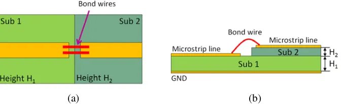
Bond wires are massively used in monolithic microwave integrated circuits (MMICs) and multi-chip modules (MCMs) for signal transmission among substrates with different heights, shown in Figure 1(a). Substrate 2 with a height of H2 is stacked on Substrate 1 with a height of H1, shown in Figure 1(b). Bond wires interconnections are used to interconnect Substrate 1 and Substrate 2.
Substrate to substrate interconnection is important on the following applications. First, for a higher isolation among transmitter, receiver and local oscillation (LO) parts of a transceiver, each part needs to be designed on a separated circuit substrate to avoid signal leakage through the shared substrate, especially the high power LO leakage to other parts. Secondly, not in every case it is possible to place all components on a circuit substrate but to place them on different circuit substrates for a complex circuit.
(a) (b)
Figure 1. Conventional substrate to substrate interconnection using single bond wire. (a) Top view and (b) side view.
Conventionally, substrate to substrate interconnection is established using bond wire, shown in Figure 1. However, a bond wire adds a low-pass element to the microwave system and limits its
Received 1 October 2015, Accepted 1 November 2015, Scheduled 5 November 2015
* Corresponding author: Bo Zhou ([email protected]).
operating bandwidth. Approaches using multiple bond wires [1–5] or compensated microstrip stubs [6– 11] can broaden the bandwidth of such interconnections, but none of them exceed 20 GHz frequencies. It is more important that compensated open stubs are used to broaden the bandwidth of bond wire interconnection in [4–7], but in most cases, the required compensated open stubs must be narrower than 0.1 mm, which is impossible to fabricate based on current printed circuit substrate (PCB) or low temperature co-fired ceramic (LTCC) fabrication process.
In this paper, a broadband interconnection using double bond wires with square-shaped DGS under open stubs has been proposed. The proposed square-shaped DGS etched under compensated microstrip open stubs not only expands its operating bandwidth, but also increases the characteristic impedance of microstrip line without narrowing its width, which breaks the PCB fabrication limitation of narrow stubs. One remarkable advantage of using the proposed structure is that it is possible to increase the characteristic impedance of microstrip line without narrowing its width. A 250 Ω characteristic impedance is easily achieved using 0.6 mm microstrip line with the proposed DGS patterned in the ground plane. The proposed interconnection also exhibits low-pass characteristics. The measured results agree well with the simulations.
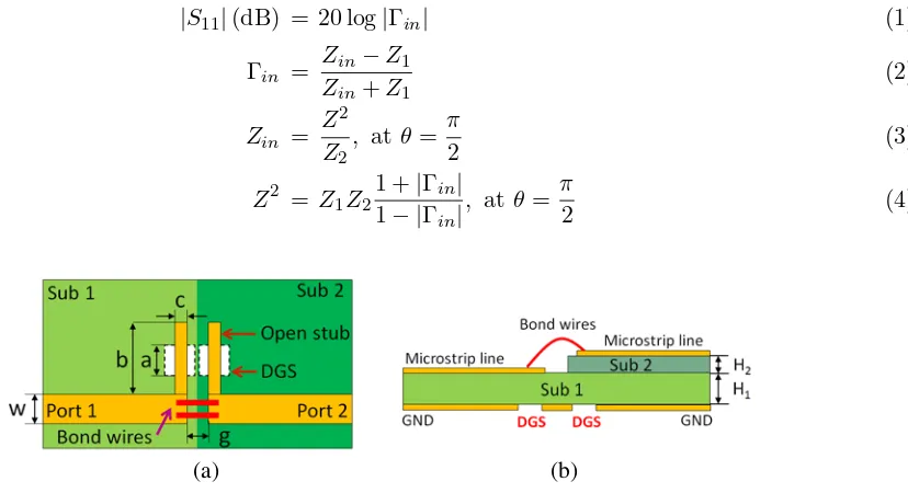
2. BROADBAND INTERCONNECTION USING BOND WIRES WITH DGS
The top and side views of the proposed interconnection are shown in Figures 2(a) and (b), respectively. The heights of Substrate 1 and Substrate 2 are 0.5 mm and 0.2 mm, respectively. And its equivalent circuit is shown in Figure 3. Bond wire is equivalent to an inductor L that jeopardizes broadband application at microwave frequency. Compensation of the bond wire inductivity L can be achieved by further adding capacitance microstrip open stubs, whose resulting circuit resembles a three-element (C1 −L−C2) low-pass structure, shown in Figure 3. After simulation with a full-wave EM-solver AXIEM [12], the highest cutoff frequency of the proposed structure (without DGS) can be achieved when the impedances of the two open stubs are both 250 Ω, which is equivalent to 0.04 mm width microstrip line on Rogers 4003C substrate with a dielectric constant of 3.38 and thickness of 0.508 mm. However, it is impossible to etch microstrip line thinner than 0.1 mm based on current PCB or LTCC fabrication process.
To solve the problem, we propose to etch square-shaped DGS under each open stub, which is helpful to achieve a higher impedance without narrowing width of open stubs. The equivalent circuit of the transmission line with the DGS can be simplified as shown in Figure 4(b). Then, using transmission line theory, impedanceZ can be determined by Eqs. (1)–(4)
|S11|(dB) = 20 log|Γin| (1)
Γin = Zin−Z1 Zin+Z1
(2)
Zin = Z 2
Z2,
at θ= π
2 (3)
Z2 = Z 1Z2
1 +|Γin|
1− |Γin|, at θ= π
2 (4)
(a) (b)
Figure 3. Equivalent circuit of the proposed interconnection.
(a) (b)
Figure 4. (a) Microstrip line with DGS and (b) simplified model for microstrip line with DGS.
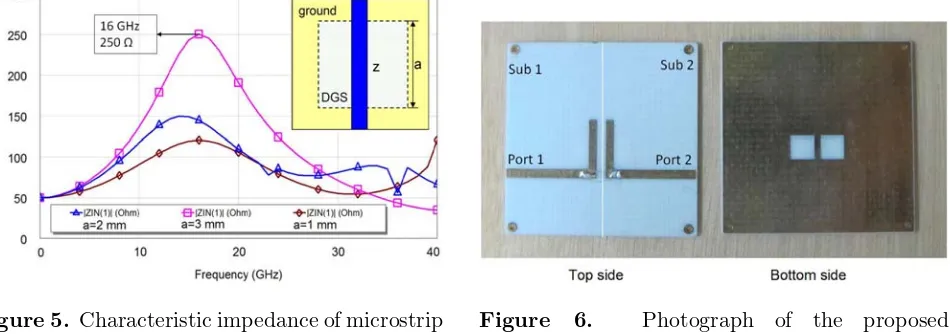
Figure 5. Characteristic impedance of microstrip line with DGS.
Figure 6. Photograph of the proposed interconnection.
When θ=π/2, the maximum magnitude of the reflection coefficient Γin is achieved. Impedance value Z with different lengths of DGS is also simulated using full-wave EM-solver AXIEM, shown in Figures 4 and 5. Parameter “a” is the length of square-shaped DGS. We can see that impedances are 120 Ω (a
= 1 mm), 150 Ω (a = 2 mm) and 250 Ω (a = 3 mm) at 16 GHz, respectively.
3. SIMULATED AND MEASURED RESULTS
(a) (b)
Figure 7. Simulated and measuredS-parameters. (a) S21 and (b)S11.
elements in Figure 3 are C1 =C2 = 0.15 pf andL = 0.26 nH.
The top and bottom views of the proposed interconnection are shown in Figure 6. Measurements are carried out by Agilent N5230C network analyzer and Cascade Microtech Summit 9000 probe stations. Measured S21 and S11 of the proposed broadband interconnection are better than −0.3 and −15 dB from DC to 38 GHz, respectively. The simulated results agree well with the measured ones, shown in Figures 7(a) and (b). We also simulated the conventional interconnection using two bond wires for comparisons (see Figure 1). The bandwidth of the proposed interconnection is 38 GHz, whereas the bandwidth of conventional interconnection is only 2.837 GHz, shown in Figure 7(b). So the proposed structure provides more than 1200% bandwidth increment compared to a conventional one.
4. CONCLUSIONS
A novel structure of broadband substrate to substrate interconnection is proposed and implemented. The proposed square-shaped DGS etched under open stubs can increase the characteristic impedance of microstrip line without narrowing its width, which is helpful to expand its operating bandwidth and break the PCB fabrication limitation of narrow stubs. Measured S21 and S11 of the proposed interconnection are better than −0.3 and −15 dB from DC to 38 GHz, respectively. And a bandwidth increment of more than 1200% is achieved compared with the conventional one.
ACKNOWLEDGMENT
The study was supported by the Nanjing University of Posts and Telecommunications Foundation (No. NY215005) and the National Natural Science Foundation of China (Nos. 61504061 & 61501261). The authors also thank AWR Corporation for making Microwave OfficeTM and AXIEMR available.
REFERENCES
1. Lee, H. Y., “Wideband characterization of mutual coupling between high density bonding wires,”
IEEE Trans. Microwave Theory Tech., Vol. 4, 265–267, 1994.
2. Lim, J. H., D. H. Kwon, J. S. Rieh, S. W. Kim, and S. W. Hwang, “RF characterization and modeling of various wire bond transitions,” IEEE Trans. Microwave Theory Tech., Vol. 28, 265– 267, 2008.
3. Wang, Z. and J. Yang, “Layout and process characteristics of LTCC substrate for microwave module,” IEEE International Symposium on Radio-frequency Integration Technology, 361–366, 2009.
5. Lee, H.-Y., “Wideband characterization of a typical bonding wire for microwave and millimeter-wave integrated circuits,”IEEE Transactions on Microwave Theory and Techniques, Vol. 43, No. 1, 63–68, 1995.
6. Chen, H.-Y. and C.-H. Tai, “Return loss of three types of arching bond wire structures for RF and microwave circuit applications,” Microwave and Optical Technology Letters, Vol. 48, No. 9, 1701–1704, 2006.
7. Zhou, B., W. Sheng, and H. Wang, “Bandwidth expansion and slow-wave effect achievement of bond wire interconnection on LTCC substrate,”Proc. IEEE Electrical Design of Advanced Packaging and Systems Symposium (EDAPS), 1–4, Hangzhou, China, Dec. 2011.
8. Lim, Y. K. and H. Y. Lee, “Novel slow-wave structure using bond-wire for miniaturizing microwave devices,” IEEE Proceeding of Asia-Pacific Microwave Conference, 1–4, 2007.
9. Zhou, B., W. Sheng, and H. Wang, “Harmonics suppression of Wilkinson power divider using bond wires with adjustable rejection bands,”Microwave and Optical Technology Letters, Vol. 54, No. 3, 775–777, 2012.
10. Zhou, B., W. X. Sheng, and H. Wang, “Slow-wave effect enhanced branch line power divider using crossing bond wires,”Electron. Lett., Vol. 47, 1246–1247, 2011.
11. Alimenti, F., P. Mezzanotte, L. Roselli, and R. Sorrentino, “Modeling and characterization of the bonding wire interconnection,” IEEE Trans. Microwave Theory Tech., Vol. 49, No. 1, 142–150, 2001.