Abstract— In this paper, a novel design of a multiband patch antenna with CPW-Fed is proposed. First, the CPW-fed conventional slot antenna is designed and then the rectangular shape is modified to achieve higher bandwidth. It covers the two bands of WLAN/WiMAX applications i.e lower band. 2.4-3.12 GHz and higher band of 5.2- 5.84 GHz. The overall size of the design is 33 mm x 23 mm x 1.6 mm with a volumetric size of 1.2
cm3. The parametric study is performed to
understand the characteristics of the proposed antenna. Also, good antenna performances such as radiation patterns and antenna gains over the operating bands have been observed. The maximum gain of the proposed antenna is 5.7 dBi at 7.9 GHz band.
Index Terms—WiMAX, WLAN, Microstrip Antenna, CPW
Feeding.
I. INTRODUCTION
Information is indeed the lifeblood of modern economies and antennas provide mother earth a solution to a wireless communication system. An antenna is a device that provides a means for radiating or receiving radio waves. In other words, it provides a transition from guided waves on a transmission line to a ―free space‖ wave (and vice versa in the receiving case). Thus information can be transferred between different locations without any intervening structure[8]Some of the antennas are Parabolic Reflectors, Patch Antennas, Slot Antennas, and Folded Dipole Antennas[1-4]. Each type of antenna is good in their own properties and usage. We can say antennas are the backbone and
Sandeep Panwar, Asstt, .Prof .Department of electronics and commuication,Haryana college of technology and management Kaithal. India,
Naresh Kumar, Asstt., .Prof .Department of electronics and commuication,Haryana college of technology and management Kaithal and Davinder Parkash, Assoc. Prof. in ECE Deptt.,Haryana College of Technology and Management, Kaithal .
almost everything in the wireless communication without which the world could have not reached at this age of technology [12]. Patch antennas play a very significant role in today‘s world of wireless communication systems.[11] A Micro strip patch antenna is very simple in the construction using a conventional Micro strip fabrication technique.[7] A Micro strip device in its simplest form is a sandwich of two parallel conducting layers separated by a single thin dielectric substrate. The upper conductor is a thin metallic patch (usually Copper or Gold), which is a small fraction of a wavelength. The lower conductor is a ground plane which should be infinite theoretically. The patch and ground-plane are separated by a dielectric substrate which is usually non-magnetic. The dielectric constant of the substrate ranges from 1.17 to about 25, with the loss tangent ranging from 0.0001 to 0.004[6]
In this paper, a novel approach to achieve a multiband antenna is introduced. The geometry of the proposed antenna is composed of the rectangular patch with two cross slot, T-cut shape slots and a small rectangle strip placed on the radiating sides of the antenna. The addition of the increases the upper edge frequency significantly resulting in a bandwidth of 1.6. The paper is organized as follows. The, section 2 presents the printed slot antenna for multiband operation and its radiation performances. After that, design and parameter study of the printed slot antennas with a cross-slotted structure and T-shape slot structure are described in Section 3. Finally paper summarized in Section 4.
II. ANTENNADESIGN
The antenna was designed on a low-cost FR4
substrate with height of hsub=1.6 mm dielectrics
constant єr=4.4 and tangent loss tanδ=.002.A
rectangular patch was chosen as the monopole radiation element. The antenna is fed by a CPW
A Novel Approach To Design CPW-Fed
Multiband Microstrip Patch Antenna for
WLAN/WiMAX applications
Volume 1, Issue 8, October 2012
transmission-line, which can be easily integrated with other CPW-based microwave printed circuits on the same substrate. The CPW feed was connected to the coaxial cable through a standard 50 SMA connector. The designed structure was simulated using IE3D simulation software .The geometry of the proposed structure is given in Figure 1.
Fig. 1 Structure of CPW-Fed microstrip patch
antenna
The designed parameters of this antenna can be stated as that length of the rectangular patch
L=29mm,width of the rectangular patch
W=16.5mm,length of the ground plane
Lg=19mm,width of the ground plane
Wg=7.5mm,length of the added slot
L1=3.5mm,length of another slot L2=7mm,width of
the both slits is W1=12mm, W2=5.6mm
L3=9.5mm,W3=2.3mm, To give feeding to this
geometry a feed line of having length Lf =22mm
and width Wf =3mm is used. The distance between
the ground plane and the rectangular patch is denoted by s that this is equal to 2mm and the distance between the feed line and ground plane is denoted by d is equal to 0.7mm. The designed antenna covers the frequency band from 2.4-3.12GHz and 5.2-5.84GHz such that total bandwidth of the proposed antenna is 1.4 GHz.Total gain of the proposed antenna 5.3 dBi at frequency 7.9 GHz.
III. RESULTS&DISCUSSION
For the proposed antenna design, IE3D simulation
software is used, which is full wave
electromagnetic simulation software for the microwave and millimeter wave integrated circuits
The results of the designed antenna shows that this antenna is covering the WLAN frequency bands 2.4 GHz and 3.1 GHz and WiMAX frequency band of 5.5 GHz .We can say that the designed antenna will be usefull for both WLAN and WiMAX applications.The following graph shows the return loss of the proposed antenna
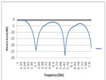
Fig. 2 Return loss of microstrip antenna
This graph shows that the designed antenna is providing the frequency from 2.4-3.12GHz and from 5.2-5.84 GHz which shows that thie designed antenna is suitable for both WiMAX and WLAN
applications.In the 1st band the return loss is -24
dBi at 2.81 GHz frequency, in the 2nd band return
Fig. 3 Radiation pattern at 5.5 GHz
Fig. 4 Radiation pattern at 2.8 GHz
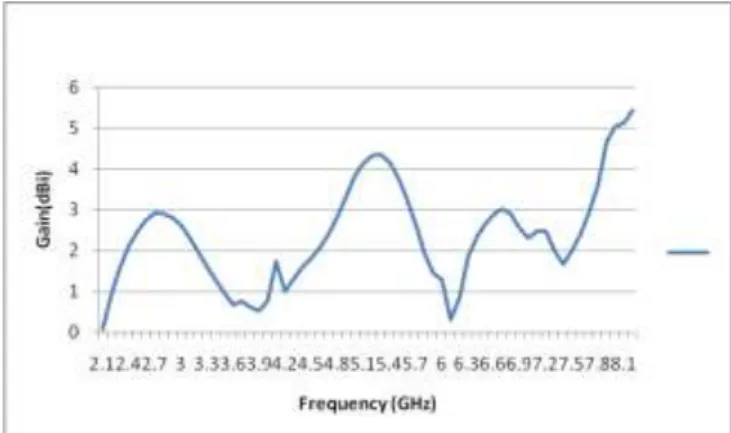
The gain of the proposed antenna is shown in
figure 5.
Fig.5 Gain characteristic of the microstrip antenna
This graph shows the gain of the dersigned antenna
is 5.3 dBi at 7.9 GHz frequency.Now the 3D
pattern of the antenna is shown in figure 6.
Fig 6 3D pattern of proposed antenna
Current Distribution Pattern: This pattern showing that how much of the current is flowing in the proposed structure.Maximum current flowing in the proposed structure is 10.47 A/m. The average current density is shown in different colors. We can see the average current distribution on the surface of the antenna. As we can observe the current is almost maximum at the centre and it is minimum at the edge of the feed line. The current
Volume 1, Issue 8, October 2012
Fig. 7 Current distribution in proposed antenna
Parametric study: In this Paper the proposed antenna is having three cuts on the radiating side of patch i.e. two cross-slot, T shape cut and a single horizontal strip cut.in this part the effect of each and every cut is analyzed .first we start with a single cross slot. which gives the total bandwidth
of 2.6 GHz.with return loss of 2nd band is
-29.1dBi.Then the another cross slot is introduced resulting in to the increase in bandwidth to 2.72 GHz. The return loss dip reaches to -47 dBi.For furher increment we added a horizontal strip cut. The bandwidth remain almost constant but return loss dip decrease to -45dBi.Then only T –cut and two cross slots are examined .which is useful and
antenna covering the actual band of
WLAN/WiMAX application .But this cost bandwidth .Bandwidth reduces to 13.4 GHz. To further increase the bandwidth horizontal strip cut is again added but it only enhance the bandwidth to 14.8 GHz. The parametric study is shown in fig 8.
Fig 8: Parametric study of the proposed antenna
IV. CONCLUSIONS
A new multiband printed microstrip antenna with CPW-fed is proposed for the WLAN/WiMAX applications. The radiation pattern is bidirectional pattern for all of operation bandwidth, The antenna has small size, the prototype antenna shows high gain. It can be observed that the peak. gain is 5.3 dBi at 7.9 GHz. There is every possibility that the overall performance of the proposed antenna can be improved in terms of size, shape, power loss, bandwidth, etc. Specially Bandwidth of the antenna .The parametric study shows that how the antenna bandwidth changes with the cut slots. The small size cost the bandwidth.
References:
[1] C. A. Balanies, Antenna Theory : Analysis
& Design, John Willey & Sons, Inc., 1997.
[2] Pozar and Schaubert, ―Microstrip
Antennas,‖ Proceedings of the IEEE, vol. 80, 1992.
[3] Kumar, G. and Ray, K. P., Broadband
Microstrip Antennas, Artech House, Inc., 2003.
[4] K. L. Wong, Compact and Broadband
Microstrip Antennas, Wiley, 2002
[5] Leena Varshney, Vibha Rani Gupta, Harishkumar, Priyadarshi Suraj,CPW-Fed Broadband Microstrip Patch Antenna‖,
International Journal of Advanced
Engineering & Application, Jan 2011 Issue-1.
―Design of A Wideband Reduced Size Microstrip Antenna In VHF/ Lower UHF Range‖ Central Mining Research Institute, Dhanbad; Instrumentation div., CMRI.
[7] Vivekananda Lanka Subrahmanya, ―
Pattern Analysis Of The Rectangular Microstrip Patch Antenna,‖ Final Master‘s Degree Thesis University College of Boras School of Engineering.
[8] Daniel Mammo, ―Design and Simulation of
Multiband Microstrip Patch Antenna for Mobile Communications,‖ School of
Graduate studies of Addis Ababa
University,September 2006.
[9] Alla I. Abunjaileh, Ian C. Hunter, Andrew
H. Kemp,‖Multi‐Band Matching
Technique for Microstrip Patch Antenna Receivers‖, School of electronic and electrical engineering, The University of Leeds‖ IEEE, EUMC.2007.4405174. [10] Yasir Ahmed, Yang Hao and Clive Parini,
―A 31.5 GHZ Patch Antenna Design for Medical Implants‖, University of London, International Journal of Antennas & Propagation‖, volume 2008, (2008), article ID 167980.
[11] S. Satthamsakul, N. Anantrasirichai, C. Benjangkapraset, and T. Wakabayashi, ‖Rectangular Patch Antenna with inset feed and modifier ground plane for wide band antennas‖, IEEE, Aug, 2008.
[12] Stutzman, W. L. and Thiele, G. A., Antenna Theory and Design, John Willey & Sons, Inc., 1998.
[13] Waterhouse, R. B., Targonski, S. D., and Kokotoff, D. M., ―Design and Performance of small Printed Antennas,‖ IEEE Trans. Antennas and Propagation, 1998, vol. 46, pp. 1629-1633.
[14] F. Yang, X-X Zhang, X. Ye and Y. Rahmat-Samii, ―Wide- Band E-Shaped
Patch Antennas for Wireless
Communications‖, IEEE Trans. Antennas and Propagat., vol. AP-49, pp. 1094– 1100, 2001 .
Davinder Parkash was born in Haryana, India in 1976. He received B.Tech. and M.Tech. degree from the Deptt. of Electronics and Communication
Engineering at Kurukshetra University,
Kurukshetra and NIT, Kurukshetra in 1999 and 2007 respectively. He is currently working toward a P.hD. degree at Thapar University, Patiala. He is currently working as Assoc. Prof. and M.Tech. coordinator at Department of Electronics and Communication Engineering at Haryana College of Technology and Management, Haryana (India). He has more than 12 years of Teaching & Research experience. Presently, he is also working as Branch-Counselor of IEEE student chapter. He
received the ‗Young Scientist Award’ from the
Governor of Punjab (India) for his research work in the field of Antenna design. He has published more than 40 papers in national and international journal/conferences. He has been also acting as Print Editor of International journal of Computer, Communication and Information Technology (IJCCIT). He has been Program Committee Member of more than 20 International/ National Conferences in India. He is Member of IEEE (Since 2010) and member of Microwave Theory and Technique society membership no.-90859628 and member of Antenna Propagation Society, Life member of Punjab Academy of Sciences, Patiala (LM-929), International Association of Engineers (IAENG), Hong Kong (L.No.- 106649) and Life member of International Association of Computer Science and Information Technology (IACSIT), Singapore [LM.No.-80344601]. His main research interest includes the analysis and design of microstrip antenna, multiband antennas, DGS
technique, RFID antenna, application of
metamaterials, MEMS and Wireless