Laser ARPES study of the
thickness-dependent electronic
structure of LaNiO
3
thin films
THESIS
submitted in partial fulfillment of the requirements for the degree of
MASTER OF SCIENCE
in PHYSICS
Author : W.O. Tromp
Student ID : 1262173
Supervisor : prof. dr. J. Aarts
2ndcorrector : prof. dr. F. Baumberger
(Universit´e de Gen`eve)
Laser ARPES study of the
thickness-dependent electronic
structure of LaNiO
3
thin films
W.O. Tromp
Huygens-Kamerlingh Onnes Laboratory, Leiden University P.O. Box 9500, 2300 RA Leiden, The Netherlands
February 19, 2018
Abstract
The family of rare-earth nickelates (RNiO3. R = La, Pr, ..., Lu) show a
sharp metal-insulator transition from a paramagnetic metal to an anti-ferromagnetic insulator. The only exception is LaNiO3which is a
paramagnetic metal even at low temperatures. Thin films of LaNiO3do
show a metal-insulator transition when reducing the film thickness to only a few unit cells. In this study we track the electronic structure of
(001) oriented LaNiO3thin films as they go from a metallic to an
insulating state. We observe this transition occurring at a thickness of 4 unit cells. The very high resolution of our ARPES set-up allows us to resolve the inelastic mean free path changing with film thickness. We find
Chapter
1
Introduction
Transition metal oxides have been the subject of intense research over the last decades. The subtle interactions between charge, spin and lattice de-grees of freedom in these compounds offer a wealth of phenomena. Of special interest are materials or families of materials showing a metal-insulator transition (MIT). The parameter space around such a transition offer an especially rich ground for exotic phenomena. The advent of new experimental tools continue to push the field forward, yielding both new fundamental insight and new technological applications.
The subject of this study, LaNiO3, is part of the rare-earth nickelates
RNiO3 (R = La, Pr, ..., Lu), which were first synthesised in 1971 by
De-mazeau et al [1]. The extreme conditions needed for the Ni3+ ionisation meant that only polycrystalline samples could be grow. New interest in the field emerged with the availability of high quality single crystal epi-taxial thin films. From first the polycrystalline samples, and later the thin films, it emerged that this family of compounds host a wide range of exotic phenomena, most pronounced of which is the sharp MIT. Other phenom-ena include charge ordering, unusual anti-ferromagnetic ordering [2][3], and the putative existence of multiferroicity [4]. The prediction of super-conductivity in LaNiO3/LaMO3superlattices has provoked large interest
in LaNiO3based heterostructures. It is only very recently that large single
crystals of LaNiO3can be grown [5][6].
6 Introduction
this is LaNiO3which is metallic and paramagnetic at all temperatures
(al-though recently some doubt has been cast on the paramagnetic nature [6]). An MIT has been observed, however, in LaNiO3thin films when the
thick-ness of the film is reduced to only a few unit cells [7]. The loss of spectral weight atEF accompanying this transition was reported to indicate a very
sudden transition between 2 and 3 unit cells thickness [8].
In this study we report the thickness-dependent electronic structure of
(001) oriented LaNiO3 probed by laser ARPES. The films were grown in
the newly installed sputtering chamber at the ARPES lab at the University of Geneva, able to transfer samples in vacuum to the analyser. The quality of the samples was characterised using a combination of X-ray diffraction, X-ray reflectrometry and transport measurements. We find the associated loss of spectral weight occurring at a thickness of 4 unit cells, in line with previous reports. We also find that the carrier mean free path and the quasi-particle peak height-to-background ratio mimic the reported con-ductivity behaviour [9]. Tracking the energy distribution near EF along
one of the Fermi surface arcs shows a pseudogap opening in the insulat-ing phase. Attempts to carry out a similar study of (111) oriented LaNiO3
thin films have thus far not proven successful.
6
Chapter
2
Theory
2.1
Mott Insulators
LaNiO3belongs to the family of rare-earth nickelates RNiO3(R = La, Pr, ...,
Lu). In the purely ionic picture, these compounds consist of R3+, Ni3+and
O2-. Interestingly, many of these compounds have an insulating ground
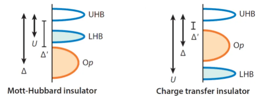
state, despite the Ni ion naively having a 3d7 configuration, implying a partially filled band. This is resolved by an idea proposed by Mott ex-ploring how strong correlation between electrons can lead to an insulating state[10]. This idea states that the electrons are strongly localised and that double occupancy on a site is penalised. A model worked out by Hubbard [11], known as the Hubbard Hamiltonian, indeed showed that electrons from a partially filled band can be localised by a sufficiently strong on-site Coulomb repulsion,U. In this model, the band structure close to the Fermi level is split in two bands, with the Fermi level sitting in the gap between the bands. The centres of the upper and lower bands, called the upper and lower Hubbard bands respectively, are separated by an energyU. There is a criticalUc so that ifU > Uc the gap forms and the system is insulating,
while forU <Uc the bands overlap and the system is metallic. A sketch of
the insulating case, known as a Mott or Mott-Hubbard insulator, is shown in figure 2.1 on the left. Transition metal oxides often fall in this category, as the transition metal ions have strongly localised d-orbitals.
In some cases the d-orbitals hybridise with the oxygen p-orbitals. In these compounds an additional energy scale is introduced, ∆, the energy scale for transferring an electron from the p-orbital to the d-orbital. When
∆ < U, the energy gap is no longer between the two Hubbard bands,
8 Theory
Figure 2.1: Schematic band structure of Mott-Hubbard insulators and charge-transfer insulators. The upper and lower Hubbard bands are represented by UHB and LHB respectively.∆is the energy difference between the centres of the upper Hubbard band and the oxygen band, while∆‘is gap between the bottom of the former and the top of the latter. Image from [12]
the right).
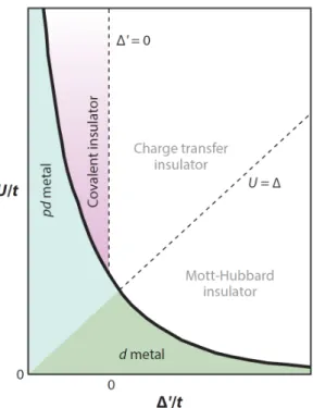
Zaanen, Sawatzky and Allen [13] combined these energy scales to sug-gest that, instead of a singleUc, a phase diagram exists withUand∆as
pa-rameters. Now the Mott-Hubbard compounds correspond toUc <U <∆,
while charge-transfer compounds correspond toU > ∆ > ∆c. The entire
phase diagram is shown in figure 2.2. As stated earlier, the model by Mott and Hubbard predicts that for small enoughU, the system becomes metal-lic. Similarly, it would seem that for small enough ∆ the effective charge
transfer∆‘ would become 0 so that the upper Hubbard band and the
oxy-gen band overlap and the system becomes metallic. Interestingly, an insu-lating state can persist even for∆‘<0, dubbed a covalent insulator. This is caused by the Hubbard band and the oxygen band being pushed apart by hybridisation of the d- and p-orbitals, similar to the bonding/anti-bonding scheme for molecular orbitals. Many intriguing materials, including the rare-earth nickelates, fall in this category. A consequence of being a cova-lent insulator, the configuration of the Ni ion is no longer purely 3d7, but a hybridisation of 3d7 and 3d8L
¯, where L¯ indicates a hole on the oxygen site. The latter state is allowed by the negative effective charge transfer∆‘ between the d- and p- orbitals.
Note that in the discussion above we have neglected the possible pres-ence of long-range order, such as charge- or spin-waves. For instance, an anti-ferromagnetic order in a lattice with half-filling can lead to an insulat-ing ground state due to doublinsulat-ing of the unit cell.
8
2.2 Metal-Insulator Transitions 9
Figure 2.2: The phase diagram based on the scheme by Zaanen, Sawatzky & Allen. Image from [12]
2.2
Metal-Insulator Transitions
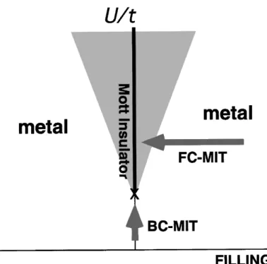
A striking feature of many transition metal oxides, and indeed most of the nickelates, is the existence of a metal-insulator transition (MIT). Here, we discuss such a transition in the context of a Mott insulator. The key parameters in describing a Mott insulator are U/t and the filling n (for a charge-transfer insulator, this would be ∆/t and n). An MIT can occur by variation of either of these parameters. Varying the interaction U is the domain of Fermi-liquid theory, which describes ground states by adi-abatically turning on the interactions. As such, one would expect in this the filling nnot to change, which was proven to be the case by Luttinger [14]. The MIT is then approached by divergence of the quasi-particle mass
m. Indeed mass enhancement has been observed in many compounds,
including the LaNiO3 [8], showing that the ground state sits close to an
MIT.
10 Theory
carrier density. This occurs for instance in anti-ferromagnetic materials showing an MIT [15].
From these arguments we can identify two types of MIT, a bandwidth-controlled MIT showing mass enhancements, and a filling-bandwidth-controlled MIT, which may or may not show mass enhancement. These two types are depicted in the phase diagram in figure 2.3. The metallic phase close to the transition ”feels” the presence of the insulating, resulting in enhanced charge, orbital and spin correlations. These manifest in, among others, enhanced mass, enhanced magnetic susceptibility and enhanced specific heat. In some cases, the Fermi-liquid description breaks down and a new theory is required (e.g. the high Tc superconductors).
Both types of MITs can be realised experimentally. Bandwidth-controlled transition can be induced by applying hydrostatic pressure, or substitut-ing atoms. This aims to increase the overlap between atomic orbitals, in-creasingtand thus decreasing the relevant parameterU/t. The nickelates are a canonical example of this type. Filling-controlled transitions can be induced by field-effect techniques, or by doping. High-Tc cuprates fall in
this category.
For a more detailed discussion of Mott insulator and MITs, the reader is referred to the extensive review by Imada, Fujimori & Tokura [15].
2.3
Nickelates
2.3.1
Ground state properties
The nickelates have a perovskite crystal structure, which has a cubic unit cell at higher temperatures (space group Pm¯3m). The ground state how-ever can have a variety of space groups. In case of the nickelates the metal-lic state has a orthorhombic structure (Pbnm) while the insulating state has a monoclinic structure (P21/n). LaNiO3is the only exception, being
metal-lic at all temperatures and having a rhombohedral (R¯3c) unit cell. Never-theless, a pseudo-cubic unit cell is very useful and commonly adopted. In this approximation, the crystal is assumed to be a perfect perovskite, with the Ni and R ions forming a body centered cubic unit cell (see figure 2.4). The cubic unit cell is distorted to either the rhombohedral, orthorhombic or the monoclinic unit cell by rotations of the octrahedra formed by the Ni and O ions.
The ground state features two unusual phenomena. The first is its magnetic ordering in the insulating state. The nickelates feature an anti-ferromagnetic ordering, except for LaNiO3which is paramagnetic. The
or-10
2.3 Nickelates 11
Figure 2.3: The MIT phase diagram. The shaded region indicates the insulating state, with the arrows showing the two types of MIT: bandwidth-controlled (BC-MIT) and filling-controlled (FC-(BC-MIT). Image from [15]
dering is peculiar in a sequence of (↑↑↓↓↑↑↓↓) consisting of ferromagnetic (111)pcplanes, where pc indicates a pseudo-cubic notation. The
accompa-nying wave vector is (1/4, 1/4, 1/4)pc or (1/2, 0, 1/2) in the orthorhombic
unit cell [16]. Each plane has one neighbouring plane with the same spin orientation and one neighbour with opposite orientation. This causes a magnetostriction resulting in an ionic displacement. The magnetic order-ing is shown in figure 2.5. It is worth notorder-ing that a recent report suggested an anti-ferromagnetic order at low temperatures in LaNiO3[6], leading to
the unusual combination of an anti-ferromagnetic metal.
The second phenomenon is charge ordering of the nickel sites. A dis-proportionation occurs on the Ni ions, resulting in two inequivalent nickel sites: 2Ni3+ →Ni3+δ + Ni3-δ, with the exact value of
δdepending on
tem-perature and the rare earth under consideration. This, together with the ionic displacement should lead to a non-zero electric polarisation along the [111]pcdirection, something that thus far has only been seen in
12 Theory
Figure 2.4: The unit cell of the rare-earth nickelates RNiO3. On the left is the
perfect perovskite cubic unit cell, in the middle the rhombohedral distorted unit cell, and on the left the orthorhombic distorrion. The oxygen ions sit and the vertices of the octahedra. Figure from [2].
Figure 2.5:The anti-ferromagnetic ordering in nickelates. Image from [17]
12
2.3 Nickelates 13
2.3.2
Metal-insulator transition in nickelates
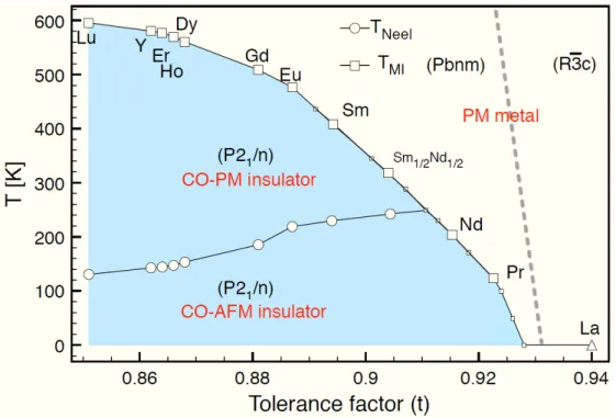
Arguably the most striking feature of the nickelates is the MIT they show. The critical temperature of this transition, TMIT is dependent on the rare
earth in question, varying from ∼130K PrNiO3 to∼600K LuNiO3,
mak-ing this a prototypical exaple of a bandwidth-controlled MIT, whose phase diagram is shown in figure 2.6. This dependence is explained by the struc-tural changes that occur when swapping rare earth ions. The size of these ions varies from one rare earth to the next, which in turn alters the angle of Ni bonds, the Ni-O-Ni angle. This angle is the main driver behind the electronic structure of the nickelates. Changes in the angle alter the over-lap between the Ni and O orbitals, hence effectively altering the hopping parameter. The transition is accompanied by a change of space group from orthorhombic to monoclinic. The induced structural changes are small, however. The exception is the largest rare earth, La, which is metallic at all temperatures, and is rhombohedral instead of orthorhombic.
Being anti-ferromagnetic, the nickelates also have a magnetic transi-tion. For the larger ions, Pr and Nd, the N´eel temperature TN coincides
with TMIT. For these ions, the transition is first-order, indicated by
hys-teretic behaviour of the resistance with temperature variation. The two phases are a paramagnetic metal and a anti-ferromagnetic insulator. For smaller ions,TN andTMITno longer coincide. There are now three phases,
going from a paramagnetic metal to a paramagnetic insulator and then a anti-ferromagnetic insulator with decreasing temperature. The different phases are indicated in the phase diagram (figure 2.6)
It has been shown that an MIT can occur in thin film LaNiO3, albeit
driven by film thickness instead of temperature [7]. Here, the transition is most likely due to structural changes in very thin film. A convenient way to describe this is by a model, shown in figure 2.7, used in the paper by Fowlie et al. [9], where they use it to describe the conductivity peak they observed. They proposed that a thin film consists of three layers with each different bond angles. First there is the interface layer, consisting of the first 2-4 unit cells, where the bond angle changes in such a way that the in-plane lattice parameter matches that of the substrate, and the Ni-O octahedra are rotated as to match the rotations in the substrate. Secondly, there is the intermediate layer, where the octahedral rotations can relax to the bulk value of LaNiO3 biaxially strained by the substrate. Finally
14 Theory
Figure 2.6: The MIT phase diagram for the nickelates. The tolerance factor is a measure of the Ni-O-Ni angle, witht = 1 being180◦. The various phases with their space group are indicated in their corresponding region. AFM, PM and CO stand for anti-ferromagnetic, paramagnetic and charge-ordered respectively. Image from [18]
thin film with a different material. This model indicates that for very thin layers, there is no intermediate layer, so that there is a structural change compared to bulk throughout the whole film. It is this structural change that drives the MIT for LaNiO3thin films.
A more detailed discussion of the properties of the nickelates can be found in the reviews by Medarde [2] and Catalan [3].
14
2.3 Nickelates 15
Figure 2.7:The three layer model proposed by Fowlie et al. Shown are the calcu-lated values for the Ni-O-Ni angles in LaNiO3films for various thicknesses. The
layers of the model are indicated by the coloured areas, with red the surface layer, yellow the intermediate layer, and green the interface layer. The dashed line in-dicates the bond angle for bulk LaNiO3biaxially strained by the substrate, here
Chapter
3
Experimental Setup
3.1
ARPES
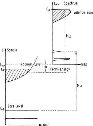
Angle-resolved photoemission spectroscopy (ARPES) exploits the photo-electric effect, in which an electron can be excited out of the sample by an incoming photon. This process is governed by the energy balance
Ekin = hν−φ−EB (3.1)
where Ekin is the kinetic energy of the excited electron, ν the frequency
of the incoming photon and EB the binding energy of the electron with
respect to the Fermi level. The work function φ is the gap in energy
be-tween the Fermi level and the energy of an electron in vacuum at rest. Measuring the kinetic energy allows for the determination of the density of statesN(E). The range of energies for which the density of states can be measured is ultimately limited by the photon energy. Using light sources with a higher frequency as a probe gains access to deeper electron states, from which a larger range of the density of states can be constructed. The photoemission process is summarised in figure 3.1.
However, the electronic structure of a material is not solely charac-terised by the density of states. In particular, thek-dependent dispersion is needed for a full characterisation. In vacuum the dispersion of the excited electron is given by
E(~k) = h¯
2(k~
k+k~⊥)2
2m (3.2)
with ~kk and k~⊥ the momenta parallel and perpendicular to the sample
18 Experimental Setup
Figure 3.1:The energy schematics of the ARPES process. The lower left shows the energetics of the sample, with the top right the energetics of the excited electron. Image from [19]
and the photoelectron suffers no scattering in the sample,k~k is conserved
during photoemission. This conservation is used to construct the band structure by relating the parallel momentum toθ, the escape angle of the
excited electron with respect to the surface normal, via
|k~k| =
1 ¯ h
p
2mEkinsinθ (3.3)
When the absence ofk⊥dispersion can be expected, as in the case of 2D or
quasi-2D materials, the full band structure can be determined. The deter-mination of dispersion along the perpendicular direction warrants a more detailed description of the photoemission process, often given in the form of the three step model.
18
3.1 ARPES 19
3.1.1
The Three step model
The three step model breaks the photoemission process up into three dis-tinct steps, and treats those steps separately. The steps are:
1. The excitation of an electron by an incoming photon.
2. Transport of the excited electron to the sample surface.
3. Escape of the electron to the vacuum.
The first step is conveniently described by Fermi’s golden rule
w ∝ 2π
¯ h |
Ψf
∆|Ψii|2δ(Ef −Ei−hν) (3.4)
Ψi and Ψf denote the state before and after excitation, with Ei and Ef
their respective energies. The perturbation∆ encodes the interaction be-tween the photon, with vector potential A~, and the electron, with initial momentum~p. The perturbation can be written as (see [19])
∆ = e
mcA~ ·~p (3.5)
Assuming the electron Hamiltonian (without coupling to photons) is given by and using the appropriate commutators
H = ~p
2
2m +V(~r) (3.6)
~
A·~pcan be written asA~ ·~p ∝ A~ · ∇V ∝ A~ ·~r. A peculiarity of this descrip-tion is that when the problem is reduced to the free electron gas (electron-electron interactionsV =const,∇V = 0), the transition ratewbecomes 0, and no photoemission occurs. This arises due to the lack of direct (i.e. ~k conserving) transitions in a free electron gas of infinite size. Refinements of the model for the electron gas will resolve this issue. The presence of theA~ and~r-dependent∆introduces dependencies on photon polarisation, photon frequency, sample geometry and orientation, all of which may af-fect the obtained spectra.
20 Experimental Setup
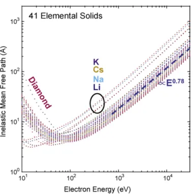
in a solid has to be added on, most easily done by introducing a complex wave vector~k. The electron mean free path is heavily dependent on its energy, whose relation is shown in fig 3.2. At a photon energy of 11eV, the
energy most commonly used in this work, the mean free path isO(1 nm),
meaning that ARPES is extremely surface sensitive. This requires clean samples and ultra high vacuum (UHV) conditions to preserve the sam-ples. Using a free electron final state gives the following expression for the perpendicular momentum:
|~k⊥| = 1
¯ h
q
2m(Ekincos2θ+V0) (3.7)
where the presence of the crystal has been absorbed in the inner potential V0. In practiceV0requires phenomenological determination.
In the third step, where the electron escapes to the vacuum, surface effects come into play. Firstly, the surface barrier has to be crossed. This is incorporated by introducing a minimum energy the final state electron has to have in order to cross the barrier. This is commonly denoted byφ,
the work function. Secondly at the surface~kkconservation is enforced.
The distinction of three steps is a very useful one, making the process tangible. However it must be kept in mind that this is a simplified model. A more correct description would be to treat the whole process in a sin-gle step using inverse LEED wavefunctions and applying a many-body description. Such a detailed analysis is beyond the scope of this thesis.
3.1.2
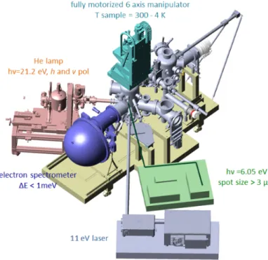
The Geneva ARPES set-up
To limit thermal broadening of spectral features, samples in the ARPES
set-ups are cooled to temperatures T ∼ 4K. Furthermore to limit
sam-ple degradation, UHV conditions are necessary. The Geneva ARPES set-up is designed to regularly operate under such conditions. To investi-gate a sample under these conditions, a three step procedure is in place. Firstly, the sample is introduced in the load lock, which can be vented with nitrogen to ambient pressure, and is pumped down to a pressure of
∼ 10−7 mbar. Then the sample is transferred to the preparation
cham-ber (pressure∼ 10−10 mbar, from which the sample can be moved to the
analysis chamber (pressure∼10−11mbar. The sputtering chamber can be accessed through the preparation chamber. The schematics of the set-up are shown in fig 3.3.
The set-up contains three light sources, an MB-Scientific He-lamp pro-ducing light with hν = 21.2 eV and hν = 40.8 eV, a 6.01 eV laser and a
20
3.2 Sputtering 21
Figure 3.2: The inelastic mean free path of electrons in various solids as function of their energy. Image from [20]
11 eV Lumeras laser. In this work the 11 eV laser is used throughout, with the exception of large energy range valence bands, for which the He-lamp was used at 21.2 eV.
A MB-Scientific A1 analyser is used for the collection and analysis of the photoelectrons. This analyser has two deflectors in place so that con-stant energy maps can be taken without rotating the sample, which is re-quired in more traditional analysers.
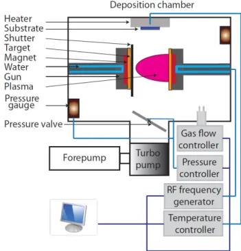
3.2
Sputtering
Techniques for depositing thin films fall into two broad categories: chem-ical vapor deposition and physchem-ical vapor deposition, the latter of which includes molecular beam epitaxy, pulsed laser deposition and sputtering. The method of choice here is radio frequency off-axis magnetron sputter-ing, where atoms are freed from the surface of a target by bombardment of heavy, positive ions of an inert gas. For a more elaborate discussion, and a discussion of other techniques, the reader is referred to the literature.
sam-22 Experimental Setup
Figure 3.3: The schematics of the Geneva ARPES set-up. The preparation cham-ber is on the righthand side of the set-up. The sputtering chamcham-ber (not shown in graphic) is attached to the preparation chamber on the right. Image from [21]
ple plate down with clamps attached to the sample holder. A target of polycrystalline LaNiO3is used. A mixture of argon and oxygen gas is
in-troduced in the chamber at a pressure of ∼ 0.18 mbar at a ratio of 3.5:1. The presence of oxygen makes sure the sample is properly oxidised to get stoichiometric samples. The gas mixture is ionised by a strong elec-tric field. To accommodate for the use of insulating targets an ac elecelec-tric field is used to prevent the build-up of charge. A strong electric field ac-celerates the ions towards the target, while a magnetic field contains the plasma. We opted for an off-axis geometry to optimise sample growth and
prevent bombardment of the sample by ions. The growth of LaNiO3
re-quires a high temperature, which is set, monitored, and controlled by a temperature controller. When not in use the sputtering chamber is kept at a pressure of∼ 10−8 mbar. This pressure can be achieved because the sputtering set-up is attached to the ARPES set-up. This allows samples to be mounted without exposing the sputtering chamber to air. As such, the sputtering chamber is opened only occasionally for maintenance or re-placement of targets. A schematic of the sputtering chamber is shown in figure 3.4.
22
3.2 Sputtering 23
Figure 3.4:The schematics of a sputtering chamber used by the group led by J-M Triscone, the design of which was the starting point of our design. Image from [18]
There are no in-situ diagnostics to monitor the quality of the film grown, so we rely on ex-situ tools. However the surface sensitivity of ARPES pre-vents us to grow a sample, take it out for diagnostics and then measure it with ARPES. Instead we first grow, then measure with ARPES and only afterwards characterise the sample.
The perovskite crystal structure of LaNiO3 necessitates the use of a
single crystal perovskite material as a subtrate to grow on. These are of-ten complex oxides, which, generally being band insulators, are also well suited for transport experiments on the films. In general, the substrates
have lattice parameters that differ from those of LaNiO3. When those
differences are small, instead of growing a LaNiO3 film with bulk lattice
parameters and defects caused by the lattice mismatch, the film will be strained so that the in-plane lattice parameter matches that of the sub-strate. This only holds up to a certain thickness, above which relaxation to the bulk structure combined with defects at the interface is energetically preferred. The substrates we opted for are SrTiO3and LaAlO3, which have
an in-plane lattice mismatch of -1.3% and +1.7% respectively [22]. For
24 Experimental Setup
thickness of∼50u.c. [18].
A common defect in oxide films are oxygen vacancies. Such vacan-cies cause lattice distortions and can alter the physical properties. The formation of these vacancies can be counteracted by an appropriate post-annealing procedure. Here, we let the sample cool down in an pure oxy-gen atmosphere of 0.18 mbar.
3.3
Sample Characterisation
We rely on several diagnostic tools to characterise our samples. We use X-ray diffraction θ - 2θ scans to identify higher order Bragg peaks, from
which the out-of-plane lattice parameter of the film can be determined. The presence of Fresnel oscillations in the diffraction pattern is indica-tive of a high quality film. Furthermore, the diffraction pattern can show the presence of crystalline contaminations. A typical diffraction pattern is shown in figure 3.5, where the main features are clearly visible. The sharp peak corresponds to the second order Bragg peak of a substrate ter-minated by a (001) plane, commonly referred to as the 002 Bragg peak. The broader peak next to it is the Bragg peak from the thin film, whose Fresnel oscillations are visible. X-ray reflectrometry is used to calibrate the film thickness. This is done by fitting the reflection pattern with the GenX software package [23], giving an absolute thickness in ˚A. Thickness in unit cells (u.c.) is then obtained by dividing the thickness in ˚A by the out of plane lattice parameter. The X-ray source used for these measurements produces the CuKα1line withλ =1.5402 ˚A.
The resistivity is measured using an Quantum Design PPMS. To do transport measurements, four platinum contacts are deposited on the sam-ple corners. This enables the use of the Van der Pauw method to determine sheet resistance. The temperature dependence of the resistivity shows whether a sample is metallic or insulating, where we define metallic as ∂ρ/∂T > 0 for all temperature T. Furthermore, the low temperature value of the resistivity for metallic samples is an indicator of sample quality.
24
3.3 Sample Characterisation 25
Chapter
4
Results
4.1
LaNiO
3films on SrTiO
3The first series of samples were grown on SrTiO3 (STO) substrates, with
one sample grown on LaAlO3(LAO) as comparison. These substrates are
terminated by a (001) plane. We started by growing a calibration sample on STO, from which we determined the growth rate, assuming linearity in time and source power. This calibration was found to be also consis-tent with growth on LAO substrates. For this sample we also determined the out of plane lattice parameter, which we used to determine the film thickness for this sample and for subsequent samples on STO. The X-ray diffraction and reflection patterns are shown in figure 4.1. The diffraction pattern in figure 4.1a shows the (001) and (002) peaks for both the STO substrate and the LaNiO3film, with the sharp peak belonging to the
for-mer and the Fresnel pattern belonging to the latter. The clear visibility of the fringes of the Fresnel pattern indicates a good sample quality. Fur-thermore, the absence of a signal between the Bragg peaks indicates that there are at most very few defects or crystalline contaminants. The out of plane lattice parameter for the film was determined to be 3.78 ˚A, which combined with the absolute thickness extracted from the oscillations in figure 4.1b gave a thickness of 44 unit cells (u.c.). The growth parameters were a power of 30W for 30 minutes.
The ARPES measurements we do fall into one of two categories. First there are the Fermi surface maps, where we measure the intensity at the Fermi level as a function of the twokk directions for a fixedk⊥. The result
is a 2D map of the cross-section of the Fermi surface and a k⊥ = const.
28 Results
(a) (b)
Figure 4.1:X-ray data of the calibration sample. Figure 4.1a shows the diffraction pattern around the (001) and the (002) peaks, and figure 4.1b shows the reflection pattern.
the otherkk. From a dispersion plot we obtain a momentum distribution
by integrating an energy window of the dispersion plot. These distribu-tion curves are fitted with Lorentzian line profiles, to get thekkvalue of the
distribution peak and the width of the distribution curve. By integrating the dispersion plot around thekkvalue of the line, we get an energy
distri-bution. From the width of the line profile we obtain the inelastic mean free path by taking the reciprocal of the line width. In this work, we present the Fermi surface maps, the energy distributions and the mean free path values of our samples.
The first series consisted of two samples on STO, one at 30W and one at 20W growth power, and one sample grown on LAO with 20W power. The X-ray diffraction patterns (figure 4.3a) indicate good sample quality, with the reflection pattern (figure 4.3b) indicating a thickness of 13 u.c., 14 u.c. and 13 u.c. respectively. The ARPES data for these samples is summarised in figures 4.4 and 4.5. The integrated spectra over a large energy range (figure 4.4a) were taken with the helium lamp (hν = 21.2eV, while the
rest of the data was taken with the 11eV laser. All of these samples show metallic behaviour in ARPES with a well defined Fermi surface (figure 4.5) and a quasi-particle peak with a sharp cut-off (figure 4.4b). To determine thekzvalue at which the Fermi surface maps were taken, we use equation
(3.7), where we take an inner potentialV0 =10 eV, as was determined by
Eguchi et al [25]. For this we obtainkz =0.56 ˚A-1. The dispersion plot cuts
were taken kz and ky = −0.23 ˚A-1, as determined by equation (3.3). The
dispersion plots show a suppression of emission at kx = 0. Rather than
being a characteristic of LaNiO3, this is the result of the laser polarisation
28
4.1 LaNiO3films on SrTiO3 29
(a) (b)
(c)
(d)
(e)
Figure 4.2:Examples of the types of data used in this work. Figures 4.2a and 4.2b show the full Fermi surface and the cross-section at kz = 0.56π/a respectively
from a two band tight binding model with parameters from [24]. The black line in 4.2b indicates where the dispersion plot 4.2c was taken. From this dispersion plot, the momentum distribution 4.2d was taken by integrating a window around EF. The energy distribution 4.2e was obtained by integrating around the peak in
30 Results
used. As noted in section 3.1.1, the observed emission may depend on polarisation, resulting here in a complete suppression. Evidence that this is a matrix element issue is shown in figure 4.13.
As shown, the sample on LAO has a higher quasi-particle peak atEF,
and shows sharper Fermi surface features, suggesting that the LAO sam-ple may be more metallic and thus of better film quality. The explanation for this is twofold. First, the out of plane lattice parameter of LAO differs less from that of LaNiO3 than the out of plane lattice parameter of STO.
Therefore the film on LAO is less strained and the Ni-O octahedra are less distorted, so the film resembles metallic bulk LaNiO3 more closely.
Sec-ondly are the charged planes that exist in LaNiO3 and LaAlO3, but do
not exist in SrTiO3. LaNiO3 (001) consists of alternating planes of(LaO)+
and (NiO)−, which carry a net charge per unit cell. The same is true for LaAlO3, having(LaO)+and AlO− planes. SrTiO3lacks this property, the
SrO and TiO planes being neutral. Growing a LaNiO3 film on STO
re-sults in a build-up of electrostatic energy, caused by a charged plane from LaNiO3being adjacent to a neutral plane from STO. This does not occur for
films on LAO, where the alternation of charged planes can be continued in the substrate. This lack of electrostatic energy allows for higher quality films on LAO. It is for these reasons that the films we grew in subsequent series were all on LAO substrates.
(a) (b)
Figure 4.3: The X-ray data for the first series of samples. Figure 4.3a shows the diffraction patterns. The base line of the the patterns do not coincide due to dif-ferent slit sizes used during the measurements. Figure 4.3b shows the reflection patterns, plus one fit generated by GenX, showing that the software is capable of producing good fits yielding a sensible thickness.
30
4.1 LaNiO3films on SrTiO3 31
(a) (b)
32 Results
(a)
(b)
(c)
(d)
Figure 4.5: ARPES data for the 14 u.c. sample on STO (figures 4.5a and 4.5b) and the 13 u.c. sample on LAO (figures 4.5c and 4.5d). The lower arches of the Fermi surface are shown on the left (kz =0.56A˚-1), with dispersion plots atky =
−0.23A˚-1shown on the right.
32
4.2 LaNiO3films on LaAlO3 33
4.2
LaNiO
3films on LaAlO
3The second series of samples consisted solely of films grown on LAO at a power of 20W. Diagnostics were performed using X-ray diffraction, X-ray reflectivity and resistivity measurements (figure 4.6). The samples were determined to have thicknesses of 4 u.c., 5 u.c., 10 u.c., and 18 u.c.. For completeness, the data of the 13 u.c. sample on LAO from the first series is added to the figures. We were unable to perform resistivity measure-ments on the 5 u.c. sample due to time constraints. Added for comparison to figure 4.6c of resistivity measurements are resistivity curves obtained by King et al. for 5 u.c. and 8 u.c. samples [8] and curves obtained by Fowlie et al. for 8 u.c. and 11 u.c. samples [9]. The measurements indi-cate that our samples are of comparable quality to those of Fowlie et al. (grown by sputtering) and of slightly worse quality than those of King et al. (grown by molecular beam epitaxy). The only outlier seems to be the 10 u.c. sample, which has a higher resistivity than expected based on the results from Fowlie et al. This can be attributed to the annealing treatment of the substrate used for this sample. Furthermore, the X-ray diffraction and reflection patterns indicate samples free of defects or crystalline con-taminations. Insulator-like behaviour occurs at a thickness of 4 u.c., which is a higher thickness than reported by King et al. for comparable temper-ature behaviour of the resistivity. This is most likely due to the difference in overall sample quality noted earlier.
The integrated spectrum of the valence band is shown in figure 4.7a, while the energy distribution near EF is shown in figure 4.7b. The latter
were taken by integrating over a small k-space window around the Fermi level crossing. (see figure 4.8). Visible in the valence bands is the overall trend, reported by King et al., of smoothing out and progression towards lower energies of the peak near EF with decreasing thickness. It is
inter-esting to note that the spectra of the 4 u.c. and the 10 u.c. samples are sim-ilar, but differ clearly from the other spectra. Distinct features of these two spectra are the lowered height of the peak at∼ −5eV, and the extra peak at
∼ −3.5eV. The substrates used for this sample underwent annealing prior to sample growth. However due to a temperature controller malfunction this was done at too high a temperature, damaging the substrate surface leading to poorer film growth. This grouping is not visible from the spec-tra near EF (figure 4.7b), instead showing the expected behaviour of the
be-34 Results
(a) (b)
(c)
Figure 4.6: Diagnostics of the samples grown on LAO. Shown are the X-ray diffraction patterns (figure 4.6a), the reflection patterns (figure 4.6b), and the re-sistivity curves (figure 4.6c). Rere-sistivity curves from King et al. [8] and Fowlie et al. [9] are included for comparison.
haviour is shown to occur in the thickness dependent conductivity, where a peak conductivity exists in a thickness range of 6-11 u.c. [9]. Should the conductivity and the quasi-particle peak height-to-background ratio be linked, we would expect the maximum relative height of the peak to occur in the 10 u.c. sample. However, the damage done by the annealing might have caused a suppression of the energy distribution peak atEF.
Figure 4.8 shows the dispersion plots at ky = −0.23 ˚A-1 and kz =
0.56 ˚A-1, showing the change in electronic structure with thickness. We find an abrupt change going from 5 u.c. to 4 u.c., showing a loss of weight atEF, a loss of quasi-particle coherence and a broadening of the band. The
abruptness of this change is in line with the findings of King et al. [8]. In our case, however, the transition occurs at a thicker 5 to 4 u.c. This may be attributed to the lower quality of our samples, as noted earlier. From the
34
4.2 LaNiO3films on LaAlO3 35
(a) (b)
Figure 4.7: Integrated spectra of LaNiO3 films on LAO substrates, taken with a 21.2eVHe-lamp (figure 4.7a) and an11eV laser (figure 4.7b).
momentum distribution atEF, the carrier mean free path can be obtained
by fitting the band with a Lorentzian line profile and taking the recipro-cal of the line width (see figure 4.2d). The variation of the mean free path across different thicknesses is shown in figure 4.8f. The mean free path shows a sharp drop coinciding with the loss of coherence shown in the dispersion plots. Furthermore there is a peak which coincides with the earlier noted maximum height of the quasi-particle peak, which seems to confirm the results of Fowlie et al. This all is in stark contrast to King et al., who report a near constant mean free path across all samples lower than the values we obtain for the metallic samples. Our ability to resolve the thickness dependent mean free path is a testament to the high k-space res-olution of our measurements. Oddly enough the residual resistance ratio, defined asρ(300K)/ρ(5K) does not mimic the behaviour of the mean free
path, or the conductivity. We are still unsure as to why this is.
We can estimate the resistivity of our samples from the ARPES data
by using the Drude model. The Fermi velocity vF of our samples can be
found through the slope of the dispersion atEF:
vF = 1
¯ h
∂E
∂k (4.1)
Using this, we can calculate a scattering time through:
τ = ξ
vF (4.2)
36 Results
(a) (b) (c)
(d) (e)
(f)
Figure 4.8: The dispersion plots atky = −0.23A˚-1, kz = 0.56A˚-1 for film
thick-nesses of 18 u.c. ( 4.8a), 13 u.c. ( 4.8b), 10 u.c. ( 4.8c), 5 u.c. ( 4.8d) and 4 u.c. ( 4.8e). Figure 4.8f shows the mean free path across the dispersion plots, and the residual resistivity ratio of the samples. The blue line indicates the constant mean free path reported by King et al.
36
4.2 LaNiO3films on LaAlO3 37
Figure 4.9: The measured low temperature resistivity and the resistivity esti-mated using the Drude model from the ARPES data.
resistivity is calculated by:
ρ = m
ne2τ (4.3)
wherenis the carrier number density, andeis the electron charge. For the
mass m we cannot use the bare electron mass, instead we use the
renor-malisation found by Nowadnick et al [26], who find m = 3.4me, withme
the bare electron mass. Since the ARPES measurement were taken at 5 K, we compare the calculated resistivity with the measured low-temperature resistivity. The result is shown in figure 4.9. We find that the Drude re-sistivity is within an order of magnitude of the measured rere-sistivity for the metallic samples, indicating that our measurements are not obviously limited by our instrument. Our estimate for the 4 u.c. sample is far off, however this is an insulating sample where we cannot expect the Drude model to give reasonable results.
The Fermi surface maps (figure 4.10) show similar behaviour, with the Fermi surface at 18 u.c. showing sharp features which get significantly broadened at 4 u.c. All of the maps and dispersion plots (figures 4.5, 4.8 and 4.10) have an asymmetry in intensity. This is an effect of the emission matrix elements being dependent on the sample orientation with respect to the laser and the detector, rather than being intrinsic to LaNiO3 thin
films.
Using the map of the 18 u.c. sample, we can track the evolution of the mean free path and the energy distribution nearEF along one of the arcs of
the Fermi surface. We measured the energy distribution at several points along the arc, indicated by the angleαbetweenkxand the line connecting
38 Results
(a) (b)
Figure 4.10: Fermi surface maps for the 18 u.c. film ( 4.10a) and the 4 u.c. film ( 4.10b) atky =−0.23A˚-1,kz =0.56A˚-1.
However, there is no movement of the Fermi level and no pseudo-gap opening. To obtain the mean free path, we measured the momentum dis-tributions across the arc. The lines along which these disdis-tributions were measured have an angle α with respect to kx so that they go through the
indicated points and the Brillouin zone corner. This means that we’ve approximated the shape of the Fermi surface by a circle, since we would ideally draw these lines perpendicular to the Fermi surface. So there is an angle difference∆α between the actual line and the ideal line. The error
this causes in the mean free path is a factor of cos(∆α). The error∆αis zero
forα = 45◦ and gets larger with decreasingα. The error is largest for the
lowest values of alpha, where the ideal line would be nearly horizontal. So for the last point,α =24.2◦, and the error is a factor of cos(24.2◦) ≈ 0.91.
So the error in the mean free path due to the approximation of the Fermi
surface shape is ∼ 10%. The mean free path evolution obtained through
this analysis is shown in figure 4.11c. The mean free path shows a com-parable trend to that of the energy distribution, with the mean free path decreasing as the Fermi surface angle decreases. This means that the mean free path is dependent on the direction in k-space, which is highly unusual for a metallic state, where normally the mean free path is isotropic. This indicates that there is some k-dependent interaction, most likely of which are phonon scattering or magnetic fluctuations. A famous example of a similar anisotropy is the pseudo-gap state of the high-Tc cuprates, where
the size of the pseudo-gap depends on the direction in k-space [27]. The same analysis is carried out for the 4 unit cell sample; the results in
38
4.2 LaNiO3films on LaAlO3 39
figure 4.12. Now we find that a pseudo-gap has opened at the Fermi level, and the size of the gap is anisotropic. Some of the energy distribution curves show some in-gap feature, however the size of these is compara-ble to the noise level in the distribution. We are therefore still doubtful whether there is actually an in-gap feature. The mean free path shows an anisotropy similar to the 18 u.c. sample. The value atα =51.0◦ is possibly
an outlier due to the fact that the peak in the momentum distribution at this angle is close to the edge of map segment we used. The combination of a pseudo-gap and a k-space anisotropy makes that this insulating sam-ple resembles the pseudo-gap state of the cuprates more closely. Whether this analogy is justified remains to be seen.
The dispersion plots (figures 4.5 and 4.8) show a suppression of emis-sion atky =0. This is a result of the polarisation dependence of the matrix
elements governing the emission process. To demonstrate this we mea-sured two cuts on the 18 u.c., one with a predominantly P polarisation, and one with a predominantly S polarisation (figure 4.13). As shown, a change of polarisation lifts the suppression and we see the band closing. We nevertheless continued to use P polarisation where there is a suppres-sion of emissuppres-sion, because the laser intensity is significantly lower in the S polarisation, resulting in less sharp peaks atEF.
As a way of optimising the growth of the films, we also treated a LAO substrate with an HCl solution and O2annealing prior to growing a 5 u.c.
40 Results
(a)
(b)
(c)
Figure 4.11: The energy distribution aroundEF( 4.11b) and the mean free path
( 4.11c) along Fermi surface arc ( 4.11a) of the 18 u.c. sample. The energy distri-butions were taken at the marked points, with the mean free paths obtained from the momentum distribution along lines through the marked points and centred at the corner of the Brillouin zone. The position of the marked points is given by the Fermi surface angleα.
40
4.2 LaNiO3films on LaAlO3 41
(a)
(b)
(c)
42 Results
(a) (b)
Figure 4.13: Dispersion plots of the 18 u.c. thin film, where the laser was P po-larised for the left dispersion plot, and S popo-larised for the right dispersion plot.
Figure 4.14: The effects of chemical treatment of the LAO substrate on 5 u.c. LaNiO3thin film.
42
4.3 LaNiO3(111) thin films 43
(a) (b)
(c)
(d)
(e) (f)
Figure 4.15: Summary of the data on STO(111) and LAO(111) samples. Fig-ure 4.15a shows the X-ray diffraction patterns of the thin films. There are two LAO peaks visible close to each other due to LAO being a twin crys-tal. Figure 4.15b shows the temperature dependent resistivity of the sample on LAO(111). Figures 4.15c and 4.15d show the valence band and the energy dis-tribution near EF respectively. The dispersion plots are shown in figures 4.15e
and 4.15f for the samples on STO(111) and LAO(111)
4.3
LaNiO
3(111) thin films
We tried growing LaNiO3films on STO(111) and LAO(111), the results of
which is shown in figure 4.15. The dispersion plots show no band struc-ture nearEF, and there is barely a presence of a quasi-particle peak. The
valence band too have only barely visible features close to EF. However,
judging by the X-ray diffraction patterns and the metallic behaviour of the resistivity, we would expect to see some features near EF similar to
44 Results
be that 11 eV happens to be a bad choice for LaNiO3 samples. For
rea-sons similar to the (001) case we expect to be able to achieve better film quality on LAO(111) compared to STO(111). Primarily because the lat-tice mismatch is less on LAO(111). Secondly, here too there is an issue of differently charged planes. In the (111) case, LaNiO3 consists of
alter-nating(LaO3)3− and Ni3+ planes, LaAlO3consists of(LaO3)3−and Al3+
planes, and SrTiO3 consists of(SrO3)4− and Ti4+. So here too there is a
charge difference per unit cell of 1 between LaNiO3 and SrTiO3, limiting
the film quality. While the valence band does show pronounced difference between the STO(111) and the LAO(111) samples, this is not reflected in the energy distribution nearEF. We believe that we are currently not
pri-marily limited by differences of the substrates, but rather by the incident photon energy.
44
Chapter
5
Conclusion & Outlook
Our aim was to map the evolution of the electronic structure of LaNiO3
thin films over varying thickness. We achieved this by growing the films in the in-situ sputtering chamber of the laser ARPES set-up at the univer-sity of Geneva. We characterised the electronic structure of the thin films by measuring dispersion plots at ky = −0.23 ˚A-1, kz = 0.56 ˚A-1.
Esti-mates of the resistivity using the Drude model suggest that our measure-ments are not primarily limited by our instrumeasure-ments. Fermi surface maps were obtained for 14 u.c. LaNiO3on SrTiO3(001) and for 4, 13, and 18 u.c.
LaNiO3 on LaAlO3(001). We observe a gradual loss of spectral weight at
EF, and a loss of quasi-particle coherence approaching a thickness 4 u.c.
of LaNiO3. Along with the changes in spectral weight, we find a drop
in the carrier inelastic mean free path, where so far only a near constant mean free path has been observed. We also find that the mean free path and the height-to-background ratio of the peak atEFmimics the
thickness-dependent behaviour of the conductivity reported by Fowlie et al [9]. The energy distribution nearEF and the mean free path were monitored along
one of the arcs of the Fermi surface for the 18 u.c. and the 4 u.c. samples. We observe an anisotropy in k-space in both samples and a pseudo-gap opening in the 4 u.c. sample. While we were able to grow films on LaAlO3
and SrTiO3 substrates, we were unable to obtain decent quality ARPES
data for these sample. We believe that the photon energy used limits the data quality for these films.
In order to prove that the transition to an insulating state is driven by the bond angles, the next step in this research would be to cap the LaNiO3
films with a thin LaAlO3layer. Using a capping layer would significantly
differ-46 Conclusion & Outlook
ent material. LaAlO3is an especially suitable choice, since the lattice
mis-match between LaAlO3is only 1.3%, and both LaAlO3and LaNiO3consist
in part of(LaO)−planes. Here, the last(LaO)− plane of LaNiO3 doubles
as the first(LaO)−plane of LaAlO3, further reduces the amount of
relax-ation needed at this interface. With this capping layer we hope to suppress the transition to an insulating state. The ultra thin metallic LaNiO3 films
in these samples are promising devices to observe a quantum well state. These states arise when one of the dimensions of a metal is reduced to be-low the mean free path in that dimension. In this case there is no longer a 3D metal but a 2D metal and a quantum well in the third direction. For
LaNiO3the film thickness would have to be reduced below the mean free
path ofO(10 nm), or below a thickness of 4 unit cells. Normally such thin samples are insulating, however by suppressing the transition using a cap-ping layer, we might be able to obtain thin enough metallic samples to see a quantum well state.
Further gains can be achieved by optimising the growth process. As observed, annealing substrates can have a pronounced effect on the thin films. Chemical treatment can impact the quality of the films in a similar way. Using these two processes, it should be possible to achieve substrates with atomically flat terraces and a single termination. We believe that an optimisation of substrate treatment can beneficially impact the thin film quality. This might also be the key to achieving good quality samples on (111) substrates.
46
Bibliography
[1] G. Demazeau, A. Marbeuf, M. Pouchard, and P. Hagenmuller, Sur
une s´erie de compos´es oxyg`enes du nickel trivalent deriv´es de la perovskite, Journal of Solid State Chemistry3, 582 (1971).
[2] M. L. Medarde and L. Medarde, Structural , magnetic and electronic
properties of perovskites ( R = rare earth ) Structural , magnetic and elec-tronic properties of RNiO 3 perovskites ( R = rare earth ), J. Phys.: Con-dens. Matter1679, 1679 (1997).
[3] G. Catalan, Progress in perovskite nickelate research, Phase Transitions
81, 729 (2008).
[4] G. Giovannetti, S. Kumar, D. Khomskii, S. Picozzi, and J. van den Brink,Multiferroicity in Rare-Earth Nickelates RNiO3, Phys. Rev. Lett.
103, 156401 (2009).
[5] J. Zhang, H. Zheng, Y. Ren, and J. F. Mitchell,High-Pressure Floating-Zone Growth of Perovskite Nickelate LaNiO3 Single Crystals, Crystal Growth & Design17, 2730 (2017).
[6] H. Guo, Z. W. Li, L. Zhao, Z. Hu, C. F. Chang, C.-Y. Kuo, W. Schmidt, A. Piovano, T. W. Pi, O. Sobolev, D. I. Khomskii, L. H. Tjeng, and A. C. Komarek, Antiferromagnetic correlations in the metallic strongly correlated transition metal oxide LaNiO3 , Nature Communications9, 43 (2018).
48 BIBLIOGRAPHY
[8] P. D. C. King, H. I. Wei, Y. F. Nie, M. Uchida, C. Adamo, S. Zhu, X. He, I. Boˇzovi´c, D. G. Schlom, and K. M. Shen, Atomic-scale control of com-peting electronic phases in ultrathin LaNiO3, Nature Nanotechnology9, 443 (2014).
[9] J. Fowlie, M. Gibert, G. Tieri, A. Gloter, J. ´I ˜niguez, A. Filip-petti, S. Catalano, S. Gariglio, A. Schober, M. Guennou, J. Kreisel, O. St´ephan, and J. M. Triscone, Conductivity and Local Structure of LaNiO3 Thin Films, Advanced Materials29, 1 (2017).
[10] N. Mott,The Basis of the Electron Theory of Metals, with Special Reference to the Transition Metals, Proc. Phys. Soc. A62, 416 (1949).
[11] J. Hubbard, Electron correlations in narrow energy bands, Proceedings of the Royal Society A276, 238 (1963).
[12] S. Middey, J. Chakhalian, P. Mahadevan, J. W. Freeland, A. J. Millis, and D. D. Sarma, Physics of ultrathin films and heterostructures of rare earth nickelates, Annuel Review of Materials Research46, 305 (2016).
[13] J. Zaanen, G. A. Sawatzky, and J. W. Allen, Band gaps and electronic structure of transition-metal compounds, Physical Review Letters 55, 418 (1985).
[14] J. M. Luttinger,Fermi Surface and Some Simple Equilibrium Properties of a System of Interacting Fermions, Phys. Rev.119, 1153 (1960).
[15] M. Imada, A. Fujimori, and Y. Tokura,Metal-insulator transitions, Re-views of Modern Physics70, 1039 (1998).
[16] J. L. Garc´ıa-Mu ˜noz, J. Rodr´ıguez-Carvajal, and P. Lacorre, Neutron-diffraction study of the magnetic ordering in the insulating regime of the perovskites RNiO3 (R=Pr and Nd), Phys. Rev. B50, 978 (1994).
[17] J. Van Den Brink and D. I. Khomskii,Multiferroicity due to charge or-dering, Journal of Physics Condensed Matter20(2008).
[18] R. Scherwitzl, Metal-Insulator transitions in nickelate heterostructures, PhD thesis, Universit´e de Gen`eve, 2012.
[19] S. Hufner, Photoelectron Spectroscopy, Springer-Verlag Berlin Heidel-berg, third edition, 2003.
48
BIBLIOGRAPHY 49
[20] C. S. Fadley,X-ray photoelectron spectroscopy: Progress and perspectives,
Journal of Electron Spectroscopy and Related Phenomena178-179, 2
(2010).
[21] A. de la Torre,Spectroscopic studies of layered iridium oxides, PhD thesis, Universit´e de Gen`eve, 2015.
[22] H. K. Yoo, S. I. Hyun, L. Moreschini, H.-D. Kim, Y. J. Chang, C. H. Sohn, D. W. Jeong, S. Sinn, Y. S. Kim, A. Bostwick, E. Rotenberg, J. H. Shim, and T. W. Noh, Latent instabilities in metallic LaNiO3 films by strain control of Fermi-surface topology, Scientific Reports5, 8746 (2015).
[23] M. Bj ¨orck and G. Andersson, GenX: an extensible X-ray reflectivity re-finement program utilizing differential evolution, Journal of Applied Crystallography40, 1174 (2007).
[24] S. Lee, R. Chen, and L. Balents,Metal-insulator transition in a two-band model for the perovskite nickelates, Phys. Rev. B84, 165119 (2011).
[25] R. Eguchi, A. Chainani, M. Taguchi, M. Matsunami, Y. Ishida, K. Horiba, Y. Senba, H. Ohashi, and S. Shin, Fermi surfaces, electron-hole asymmetry, and correlation kink in a three-dimensional Fermi liq-uid LaNiO3, Physical Review B - Condensed Matter and Materials Physics79, 1 (2009).
[26] E. A. Nowadnick, J. P. Ruf, H. Park, P. D. King, D. G. Schlom, K. M. Shen, and A. J. Millis, Quantifying electronic correlation strength in a complex oxide: A combined DMFT and ARPES study of LaNiO3, Physical Review B - Condensed Matter and Materials Physics92, 1 (2015).