Leakage Reduction Using DTSCL and Current Mirror
SCL Logic Structures for LP-LV Circuits
Sanjeev Rai1, Ram Awadh Mishra1, Sudarshan Tiwari2
1Department of Electronics & Communication Engineering, Motilal Nehru National Institute of Technology Allahabad,
Allahabad, India
2National Institute of Technology, Raipur, India
Email: [email protected], [email protected], [email protected]
Received September 3, 2012; revised October 5, 2012; accepted October 13, 2012
ABSTRACT
This paper presents a novel approach to design robust Source Coupled Logic (SCL) for implementing ultra low power circuits. In this paper, we propose two different source coupled logic structures and analyze the performance of these structures with STSCL (Sub-threshold SCL). The first design under consideration is DTPMOS as load device which analyses the performance of Dynamic Threshold SCL (DTSCL) Logic with previous source coupled logic for ultra low power operation. DTSCL circuits exhibit a better power-delay Performance compared with the STSCL Logic. It can be seen that the proposed circuit provides 56% reduction in power delay product. The second design under consideration uses basic current mirror active load device to provide required voltage swing. Current mirror source coupled logic (CMSCL) can be used for high speed operation. The advantage of this design is that it provides 54% reduction in power delay product over conventional STSCL. The main drawback of this design is that it provides a higher power dissipa-tion compared to other source coupled logic structures. The proposed circuit provides lower sensitivity to temperature and power supply variation, with a superior control over power dissipation. Measurements of test structures simulated in 0.18 µm CMOS technology shows that the proposed DTSCL logic concept can be utilized successfully for bias cur- rents as low as 1 pA. Measurements show that existing standard cell libraries offer a good solution for ultra low power SCL circuits. Cadence Virtuoso schematic editor and Spectre Simulation tools have been used.
Keywords: CMOS Integrated Circuits; CMOS Logic Circuit; Dynamic Threshold MOS (DTMOS); Power-Delay
Product; Source-Coupled Logic (SCL); Sub-Threshold CMOS; Sub-Threshold SCL; Ultra-Low-Power Circuits; Weak Inversion LP-LV(Low Power-Low Voltage)
1. Introduction
The ever increasing attention on power consumption in circuit design has motivated a significant investigation of optimum design for minimizing energy or power for a given performance constraint. Technology scaling results in a significant increase in leakage current of CMOS de- vice. Various methods and techniques, such as voltage scaling, clock gating, etc. [1-3] have been applied suc- cessfully in the medium power, medium performance region of the design spectrum for lower power consump- tion. Nevertheless, in some applications where ultra-low power consumption is the primary requirement and per- formance is of secondary importance, a more aggressive approach is warranted. Special circuit techniques have been implemented to enable operation at very low cur- rent levels and to achieve the desired performance speci- fications.The demand for implementing ultra-low-power digital systems in many modern applications such as mo- bile systems [4], sensor networks [5,6], and implanted
biomedical systems [7], has increased the importance of designing logic circuits in sub-threshold regime [8].
The power dissipation is a crucial parameter in ultra- low power application. The supply voltage VDD is gener- ally reduced below the threshold voltage VT of metal- oxide-semiconductor (MOS) devices [9]. Reducing the supply voltage or choosing high-threshold-voltage (HVT) devices results in a smaller Veff = VDD− VT value and, hence, less power consumption [10]. However, reducing Veff results in reduction in the ratio of the ON-current of
a logic gate ION to its leakage current IOFF. Reduction in ON OFF
I I
plored [9]. In mixed mode integrated circuits the crucial parameters that affect the performance of the digital sys- tem are supply noise and substrate noise. Source coupled logic (SCL) are widely used to reduce the output voltage swing compared to CMOS logic gates for high frequency application. This paper explores performance comparison of two source coupled logic structures with previously available Sub Threshold Source Coupled Logic (STSCL) gates for implementing ultra-low-power digital systems. In this approach, the power consumption and maximum speed of operation can be adjusted linearly through the tail bias current of each gate over a very wide range [11,12], thus, efficiently decoupling the decision of out- put voltage swing from power dissipation and delay. To enable the operation at very low trail bias current and to achieve the desired performance, we have to use a spe- cial circuit technique for implementing very low power Source Coupled Logic circuit. In first design, the intrin- sically limited output impedance of deep-submicron, dy- namic threshold PMOS devices have been used to im- plement very high value load resistances for SCL topol- ogy. In second design an active load current mirror has been used to implement very high value of load resis- tance called Current Mirror Source Coupled Logic (CMSCL). Here, a more general approach with much less sensitivity to process and technology variations will be introduced [12]. This paper presents two different techniques, one for implementing Dynamic Threshold Source Coupled Logic (DTSCL) gates where the bias current of each cell can be set as low as 0.1 pA and an- other for implementing Current Mirror source coupled logic gates where the bias current of each cell can be set as high as 1 mA. In Section 2, after a brief review of SCL circuits, the proposed techniques for implementing dif- ferent SCL gates will be introduced. Section 3 discusses about the load device concept applied to SCL circuits. Section 4 discusses about the experimental results and implementation of the proposed circuits. Section 4.4 dis- cusses the power-delay performance of the proposed cir- cuit configurations and comparison of different SCL logic structures, followed by conclusions in Section 4.5 and finally Acknowledgement in Section 5.
2. Different Source-Coupled Logic Structure
2.1. DTMOS Topology
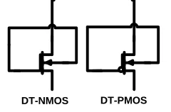
In DTMOS logic, gates of transistors are tied to their substrates to achieve the same stability with direct sub- strate biasing without using additional control circuitry as in case of VTCMOS logic (Figure 1) [11]. As the sub-
strate voltage in DTMOS logic changes with the gate input voltage, the threshold voltage is dynamically changed. In the off-state, i.e., in in DD for NMOS (PMOS), the characteristics of DTMOS transistor is exactly the same as regular MOS transistor. Both have
the same properties, such as the same off-current, sub- threshold slope, and threshold voltage. In the on-state, however, the substrate-source voltage (Vbs) for NMOS (PMOS), the characteristics of DTMOS transistor is ex- actly the same as regular MOS transistor. When the DTMOS is in off state then it offers higher threshold voltage which in turn reduces the leakage current of the MOS device. In the on state, the substrate-source voltage (Vbs) increases which in turn reduces threshold voltage of the DTMOS. Reduction in threshold voltage is due to the reduction in body charge which again leads to an advan- tage of higher carrier mobility because the reduced body charge causes a lower effective normal field. The re- duced threshold, lower normal effective electric field, and higher mobility results in higher on current drive in DTMOS than that of a simple MOS transistor.
The sub-threshold slope of DTMOS improves and ap-proaches the ideal 60 mV/decade which makes it more efficient in sub threshold logic circuits to obtain higher gain.
2.2. Current Mirror Topology
A current mirror is a circuit designed to copy a current through one active device by controlling the current in another active device of a circuit, keeping the output current constant regardless of loading. The current being ‘copied’ can be, and sometimes is, a varying signal cur- rent. Conceptually, an ideal current mirror is simply an ideal current amplifier. The current mirror is used to pro- vide bias currents and active loads to circuits. High-per- formance current mirrors with low input and output voltages are required as building blocks of mixed-mode VLSI systems that operate from a single supply of 1.8 V or below. High accuracy requires very high output resis- tance and low input resistance. Low-voltage operation requires low input and output voltages as well as low supply requirements for the control circuitry used to im- prove the mirror’s input and output resistance. There are three main specifications that characterize a current mir- ror. The first is the current level it produces. The second is its AC output resistance, which determines how much the output current varies with the voltage applied to the mirror. The third specification is the minimum voltage drop across the mirror necessary to make it work prop- erly. This minimum voltage is dictated by the need to keep the output transistor of the mirror in active mode.
0
V V V
[image:2.595.368.488.644.723.2]DT-PMOS DT-NMOS
The range of voltages where the mirror works is called the compliance range and the voltage marking the boun- dary between good and bad behavior is called the com-pliance voltage. There are also a number of seconddary performance issues with mirrors, for example, tempera- ture stability.
2.3. Basic SCL Topology
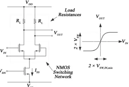
[image:3.595.61.287.562.715.2]The source coupled logic (SCL) topology has been a modern approach for designing of ultra low power cir- cuits. This topology is very suitable for very low bias current operations as it provides accurate control on power consumption of each gate, where as the power dissipation of conventional static CMOS circuits is lim- ited by their sub-threshold leakage current. Simultane- ously, the gate delay in this configuration does not de- pend on the supply voltage and hence, there is low sensi- tivity to supply voltage variations.
Figure 2 shows that the switching part can be com-
posed of a network of NMOS source-coupled pairs to implement more complex logic functions [2]. The load resistances can be implemented using PMOS devices biased in triode region.
In an SCL gate, the logic operation takes place mainly in current domain. Therefore, the speed of operation can be inherently high. The voltage swing at the output node
SW SS L should be SW n T ( n
V I R
4n UU
V n is the
sub-threshold slope factor of NMOS differential pair devices, and T is the thermal voltage). To achieve the required voltage swing at very low trail bias current the load resistance should be very high, and also occupy a small area with a very good control to adjust their re- sistivity with respect to their trail bias current. In first design, DT-PMOS transistor can be used to provide high resistance with a relatively high voltage swing at the output, the proposed topology can operate properly as logic device. In the second design, current mirror active load is used as a load device to provide higher resistance with a relatively high voltage swing.
Figure 2. A conventional SCL-based inverter/buffer circuit.
In SCL topology the main leakage currents are due to the p-n junctions of the MOS devices, whereas in CMOS logic circuits the sub-threshold channel leakage current is the dominant leakage component,. The speed of ope- ration in an SCL gate is mainly limited by the time con- stant at the output node which is calculated as Equation (1):
SCL L L SW SS
T R C V CL I (1) Based on the above, the propagation delay is inversely proportional to the tail bias current. Meanwhile, the cir- cuit power-delay product (PDP) is independent of ISS [12-14].
3. Load Device Concept
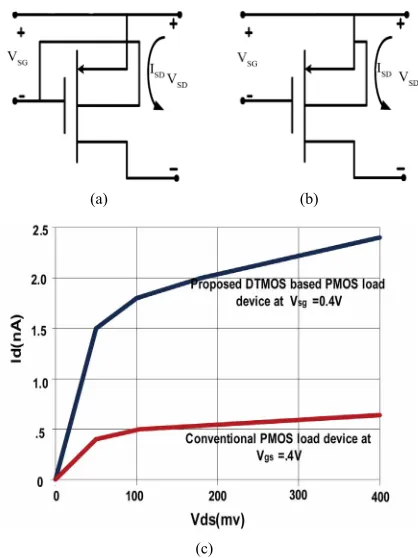
To maintain the required voltage swing at very low trail bias current it is necessary to increase the load resistance in inverse proportion to the reducing trail bias current. In sub-threshold region, the trail bias current would be in the order of few pA or even less. Therefore, to obtain a required output voltage swing, the load resistance should be of the order of few GΩ. Meanwhile, this resistance should be controlled very accurately based on the value of trail bias current ISS. Hence, a well controlled high resistivity load device with a very small area is required. For this range of resistivity, conventional PMOS devices biased in triode region cannot be utilized since the re- quired channel length of the transistor would be im- practically large. Figure 3(a) shows the proposed load
device, where the gate of the PMOS device is connected to its bulk where as Figure 3(b) is the conventional de-
vice. In this way, the load device provides accurate con- trol on the resistance, which, associated with the trans- conductance of the differential pair will provide a con- trolled, limited gain and amplitude with relatively small size PMOS load device.
Figure 3(c) shows the I-V characteristics of the
con-ventional PMOS and the proposed PMOS load device. In the proposed load device the gate and substrate of PMOS load device are shorted. When VSG = VSDthen it will behave as conventional PMOS load device as we vary the gate voltage VSG the voltage across the substrate terminal also varies as a result the threshold voltage of the device changes and also the resistance of the PMOS load device varies. In this way the proposed load device will be used as a controlled resistance.
The basic current mirror can also be implemented us- ing MOSFET transistors, as shown in Figure 4. Transis-
tor M1 is operating in the saturation or active mode, and
so is M2. In this setup, the output current IOUT is directly
related to IREF. The drain current of a MOSFET ID is a function of both the gate-source voltage and the drain- to-gate voltage of the MOSFET given by
,
D GS DG , a relationship derived from the func- tionality of the MOSFET device. In the case of transistor
(a) (b)
(c)
[image:4.595.70.279.80.359.2]Figure 3. (a) Conventional PMOS load device; (b) DT-PMOS load device; (c) I-V characteristics of the conventional PMOS load in comparison to the proposed DT-PMOS de-vice.
Figure 4. Basic Current Mirror Structure.
M1 of the mirror, ID = IREF. Reference current IREF is a known current, and can be provided by a resistor as shown, or by a “threshold-referenced” or “self-biased” current source to ensure that it is constant, independent of voltage supply variations.
Using VDG= 0 for transistor M1, the drain current in M1
is D GS DG , so we find: GS REF
The drain-to-source voltage can be expressed as DS DG GS
V V V
GS, DG
f V V
. With this substitution, the
Shichman-Hodges model Equation (2) provides an ap- proximate form for function :
V ,V 0
,0
I f f V I ,
implicitly determining the value of VGS. Thus IREF sets the
value of VGS. The circuit in the diagram forces the same VGS to apply to transistor M2. If M2 also is biased with
zero VDG and provided transistors M1 and M2 have good
matching of their properties, such as channel length, width, threshold voltage etc., the relationship IOUT = f(VGS, VDG = 0) applies, thus setting IOUT IREF ; that is, the output current is the same as the reference current when VDG= 0 for the output transistor, and both transistors are matched.
2
2
1
, 1
2 1
1 2
d
GS DG p GS th DS
p GS th DG GS
I
W
f V V K V V V
L W
K V V V V
L
(2)
where, Kp is a technology related constant associated with the transistor, W L is the width to length ratio of the transistor, VGS is the gate-source voltage, Vth is the threshold voltage, λ is the channel length modulation constant, and VDS is the drain source voltage. Because of channel-length modulation, the mirror has a finite output (or Norton) resistance given by the ro Equation (3) of the output transistor, namely
1 DS
N o
D V
R r
I
(3)
where λ is the channel-length modulation parameter and VDS is the drain-to-source bias.
4. Proposed Implementation of DTSCL &
Current Mirror SCL Gates & Results.
4.1. DTSCL Gates
[image:4.595.124.211.420.503.2]The proposed DTPMOS load device can be utilized to implement an SCL gate biased in sub-threshold regime.
Figure 5 shows the basic structure of the proposed
DTSCL gate. The Figure 5 includes the replica bias cir-
cuit which is used to control the output voltage swing. Replica bias circuit consist of two major component one is op-amp and another is a current mirror circuit which
[image:4.595.313.538.534.707.2]will maintain a constant trail bias current ISS. This circuit also tracks the variations on temperature and supply voltage and, hence, compensates their effect on the cir-cuit performance.
A simplified circuit diagram of the replica bias circuit used to control the output voltage swing is also shown. In this schematic, all devices operate in sub-threshold re- gime and the tail bias current can be reduced until it be- comes comparable in magnitude to the leakage currents that exist in the circuit. Figure 6(a) illustrates the DC
transfer characteristics of a DTSCL gate. The stage gain of DTSCL gate is as shown in Figure 6(b). The meas-
ured stage gain of DTSCL gate is approximately 42. The measured input-output transfer characteristics of a DTSCL buffer stage at different trail bias current are shown in
Figure 6(c). As all the devices are operating in sub-
threshold regime hence the transfer characteristic of the circuit is independent of the trail bias current.
In the plot above, the deviation from the ideal DC characteristics is mainly due to the leakage currents in the test circuit coming from electrostatic discharge (ESD) protection circuitry. To measure the DC characteristics, output voltage swing has been adjusted manually.
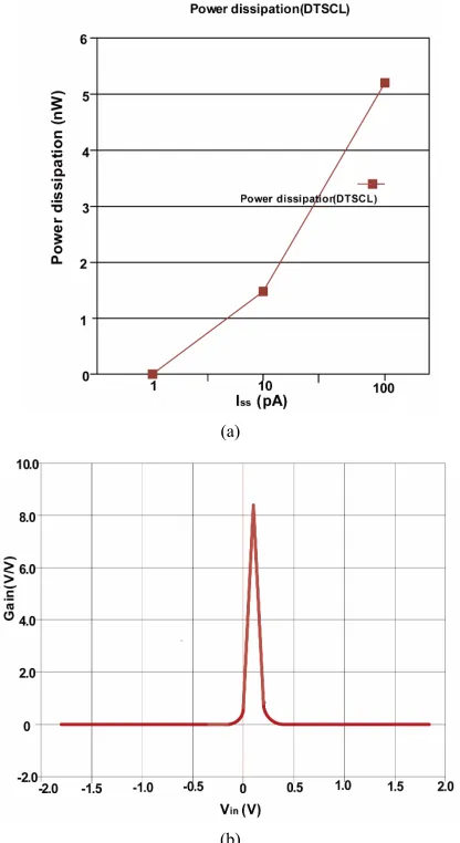
The variation in power dissipation and gate delay of a DTSCL gate is as shown in Figures 7(a) and (b)
simul-taneously. It is seen that the stabilized output of is achieved at trail bias current ISS = 1 pA. At this trail bias current, DTSCL provides lowest power delay product of the order of 569.71 × 10⁻¹⁸ W-Sec.
The Table 1 above describes the variation in delay
with different trail bias current with subsequent power dissipation and the corresponding PDP.
4.2. Current Mirror SCL Gates
The proposed current mirror active load device can be utilized to implement an SCL gate biased in sub- threshold regime. Figure 8 shows the basic structure of
the proposed Current Mirror SCL gate.
In this schematic given below, all devices operate in sub-threshold regime and the tail bias current can be re-duced until it becomes comparable in magnitude to the leakage currents that exist in the circuit.
Figure 9(a) illustrates the DC transfer characteristics
of a Current Mirror SCL gate. The stage gain of Current Mirror SCL gate is as shown in Figure 9(b). The meas-
ured stage gain of Current Mirror SCL gate is approxi- mately 8.2. The measured input-output transfer charac- teristics of a Current Mirror SCL buffer stage at different trail bias current are shown in Figure 9(c). As all the de-
vices are operating in sub-threshold regime hence the transfer characteristic of the circuit is independent of the trail bias current.
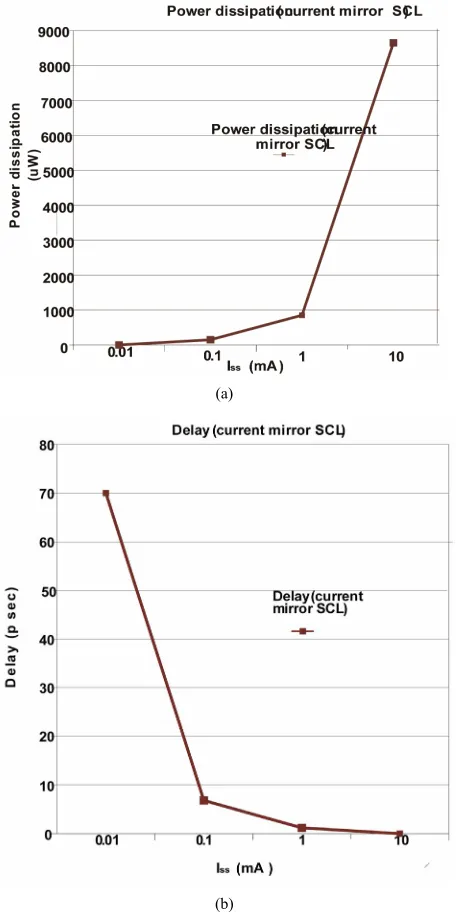
The variation in power dissipation and gate delay of a
(a)
(b)
(c)
Figure 6. (a) Simulated DC transfer characteristics of a DTSCL gate biased at ISS of 1 Pa; (b) DC gain of a DTSCL
gate biased at ISS 1 pA; (c) Measured transfer
characteris-tics of a DTSCL buffer stage for different bias currents (ISS
= 1 pA, and 10 pA).
Table 1. Variation in delay with trail bias current.
Bias current
ISS (pA) Dissipation (nW)Power Delay (n sec) PDP(10^-18 Wsec)
1 0.1096 5200 569.71
10 1.5232 900 1370.88
(a)
(b)
[image:6.595.317.528.83.607.2]Figure 7. (a) Variation in power dissipation with trail bias current; (b) Variation in delay with trail bias current.
Figure 8. Current Mirror SCL gate and the replica bias circuit used to control the output voltage swing.
(a)
(b)
(c)
Figure 9. (a) Simulated DC transfer characteristics of a Current Mirror SCL gate biased at ISS of 1 mA; (b) DC
gain of a Current Mirror SCL gate biased at ISS of 1 mA; (c)
Measured transfer characteristics of a Current Mirror SCL buffer stage for different bias currents (ISS = 1 nA, 1 µA and
1 mA).
Current Mirror SCL gate is as shown in Figure 10(a) and (b) simultaneously. It is seen that the stabilized output of
[image:6.595.68.276.86.467.2] [image:6.595.57.288.509.703.2]delay product of the order of 592.238 × 10⁻¹⁸ W-Sec.
The Table 2 Describes the PDP and power consump-
tion at different trail bias currents.
(a)
(b)
[image:7.595.60.288.132.588.2]Figure 10. (a) Variation in power dissipation with trail bias current; (b) Variation in delay with trail bias current.
Table 2. Variation in delay with trail bias current.
Bias current ISS (mA)
Power
Dissipation (µW) Delay (p sec) PDP(10^ - 18 Wsec)
0.01 16.44 70 1150.8
0.1 111.147 7.5 833.60
1.0 832.73 0.716 592.238
10 8426.12 0.0731 615.949
4.3. Voltage Swing Control
To achieve the required voltage swing at the output, a controlling circuit is used. Figure 11 shows a simplified
schematic of replica bias circuit to control the output voltage swing. The Replica bias circuit consists of a high performance current mirror circuit that can maintain a constant current ISS at the output to provide accurate control on the output voltage swing. The replica bias circuit should be well matched to the SCL gates to have very low deviation in operating point. Meanwhile, amplifier should provide enough gain with a very low offset to have the desired accuracy.
In this work, a folded-cascode amplifier has been used to provide a large swing at the output node and to be able to test the SCL gates in a very wide range of bias current values. Any mismatch in the bias current of the devices of the SCL gates and RB circuit will result in variation of the desired output voltage swing.
4.4. Performance Analysis and Observation
4.4.1. Power-Speed Trade-Off in SCL Circuits
In contrast to the CMOS gates, where there is no static power consumption (neglecting the leakage current), each SCL gate draws a constant bias current of ISS from a
supply source (Figure 2). Therefore, the power con-
sumption of each SCL gate can be calculated by Equa- tion (4) as
,SCL
diss DD SS
P V I (4) Meanwhile, the time constant at the output node of each SCL gate, is given as Equation (5) i.e.,
L L SW SS L
R C V I C
[image:7.595.323.524.527.716.2] (5) is the main speed-limiting factor in this topology (CLis the total output loading capacitance). Based on (5), one
[image:7.595.57.287.643.737.2]can choose the proper ISS value to operate at the desired frequency. This circuit exhibits a very low sensitivity to the process variations because the power consumption and delay of each gate only depend on ISS, which can very precisely be controlled. Meanwhile, it is not neces- sary to use special process options to have low threshold voltage devices, as frequently used for static CMOS [1,2,8]. Therefore, it is necessary to use the DTSCL cir- cuits at their maximum activity rate to achieve the maxi- mum achievable efficiency. It is also important to note that the gate delay does not depend on the supply voltage, whereas it linearly varies with the tail bias current. This property can be exploited for applications in which the supply can vary during the operation. Based on Equa-tions (4) and (5), the power-delay product (PDP) of each gate can be approximately calculated by Equation 6 given below:
DTSCL1ln 2V V CDD SW L
PDP (6) Observation 1:The delay of a logic block can be con- trolled without influencing PDP as the delay of DTSCL gate depends on trail bias current (ISS), but not on supply voltage VDD.
Observation 2:To reduce the power to frequency ratio,
α should be kept as large as possible. This observation does not contradict with similar results for conventional CMOS.
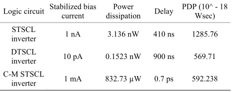
4.4.2. Tabulated Comparison of Different SCL Circuit
Shown below is the comparison of the power consump- tion, delay and power delay product of different SCL structures (STSCL, DTSCL, Current Mirror SCL) as shown in Table 3. The table shows that if we wish to
design a circuit with low power dissipation than pro- posed DTSCL is preferred over other SCL techniques and if we choose to design a circuit with higher speed than proposed Current Mirror SCL is preferred over other SCL techniques.
4.5. Conclusion
[image:8.595.57.289.646.738.2]In this paper, an analytical approach for studying and comparing the performance of ultra low power STSCL, DTSCL, and Current Mirror SCL has been presented.
Table 3. Comparison of various SCL circuits.
Logic circuit Stabilized bias current dissipation Power Delay PDP (10^ - 18 Wsec)
STSCL
inverter 1 nA 3.136 nW 410 ns 1285.76 DTSCL
inverter 10 pA 0.1523 nW 900 ns 569.71 C-M STSCL
inverter 1 mA 832.73 µW 0.7 ps 592.238
While there is a tight tradeoff among the power con- sumption, speed of operation , and supply voltage in de- sign of CMOS digital circuits, the SCL topology provide a more flexible deign option for ultra low power applica- tions. In this work, two new source coupled logic design has been discussed. The first design uses a high resis- tance DT-PMOS load device to provide the required voltage swing at the output. The measurement result shows that the DTSCL topology provides 56% reduction in PDP compared to STSCL, using 0.18 µm CMOS tech- nology. The second design uses basic current mirror load device to provide required voltage swing at the output. This design can be used for high speed operation at the cost of higher power dissipation. Hence this design can be used for high speed operation at the cost of power dissipation. The measurement result shows that the Cur- rent Mirror SCL provides 54% reduction in PDP com- pared to STSCL, using 0.18 µm CMOS technology. The trail bias current of each gate can be reduced to less than 0.1 pA, while the power delay product of the gate re- mains less than 1 FJ. The bias current of a SCL gate can be scaled over several decades, which makes this topol- ogy very suitable for ultra low power applications. The main advantage of this topology is that there is no effect of process and temperature variation and it can operate in a wide range of frequency. The author has used Cadence Virtuoso Schematic Editor [15] and Spectre as simula-
tion platform. All the results and their verification has been done by using cadence tools.
5. Acknowledgements
The authors duly acknowledged with gratitude the su- pport from ministry of communication and information technology, DIT Govt. of India, New Delhi, through spe- cial manpower Development program in VLSI and re- lated Software’s Phase-II (SMDP-II) project in ECE De- partment, MNNIT Allahabad-211004, India.
REFERENCES
[1] A. Tajalli and Y. Leblebici, “Leakage Current Reduction Using Sub-Threshold Source-Coupled Logic,” IEEE Trans- actions on Circuits and Systems—II: Express Briefs, Vol. 56, No. 5, 2009, pp. 374-378.
[2] A. Tajalli, E. J. Brauer, Y. Leblebici and E. Vittoz, “Sub-Threshold Source-Coupled Logic Circuits for Ultra- Low Power Applications,” IEEE Journal of Solid-State Circuits, Vol. 43, No. 7, 2008, pp. 1699-1710.
doi:10.1109/JSSC.2008.922709
[3] D. Suvakovic and C. A. T. Salama, “A Low Vt CMOS
Implantation of an LPLV Digital Filter Core for Portable Audio Applications,” Transactions on Circuits Systems, II: Analog and Digital Signal Processing, Vol. 47, No. 11, 2000, pp. 1297-1300.
Nano-meter CMOS,” International Symposium on Signals, Circuits and Systems, Vol. 1, Iasi, 13-14 July 2007, pp. 1-2. doi:10.1109/ISSCS.2007.4292635
[5] B. A. Warneke and K. S. J. Pister, “An Ultra-Low Energy Microcontroller for Smart Dust Wireless Sensor Net- works,” IEEE International Solid-State Circuits Confer- ence, Vol. 1, 2004, pp. 316-317.
[6] L. S. Wong, et al., “A Very Low-Power CMOS Mixed- Signal IC for Implantable Pacemaker Applications,” IEEE Journal of Solid-State Circuits, Vol. 39, No. 12, 2004, pp. 2446-2456. doi:10.1109/JSSC.2004.837027 [7] E. Vittoz, “Weak Inversion for Ultimate Low-Power
Logic,” In: C. Piguet, Ed., Low-Power Electronics Design, CRC Press, Boca Raton, 2005.
[8] B. H. Calhoun, A. Wang and A. Chandrakasan, “Model- ing and Sizing for Minimum Energy Operation in Sub- Threshold Circuits,” IEEE Journal of Solid-State Circuits, Vol. 40, No. 9, 2005, pp. 1778-1786.
doi:10.1109/JSSC.2005.852162
[9] M. Anis and M. Elmasry, “Multi-Threshold CMOS Digi- tal Circuits, Managing Leakage Power,” Kluwer, Norwell, 2003. doi:10.1007/978-1-4615-0391-0
[10] E. Brauer and Y. Leblebici, “Semiconductor Based High- Resistance Device and Logic Application,” European Patent Application No. 07104895.3-1235, 2007.
[11] H. Soeleman, K. Roy and B. C. Paul, “Robust Sub- threshold Logic for Ultra Low Power Operation,” IEEE Transactions on Very Large Scale Integration (VLSI) Systems, Vol. 9, No. 1, 2001, pp. 90-99.
[12] F. Cannillo and C. Toumazou, “Nano-Power Sub-Threshold Current-Mode Logic in Sub-100 nm Technologies,” IEEE Electronics Letters, Vol. 41, No. 23, 2005, pp. 1268-1269. doi:10.1049/el:20053082
[13] A. Tajalli, E. Vittoz, Y. Leblebici and E. J. Brauer, “Ultra Low Power Sub-Threshold MOS Current Mode Logic Circuits Using a Novel Load Device Concept,” Pro- ceedings of the European Solid-State Circuit Conference, Munich, September 2007, pp. 281-284.
[14] M. Horowitz, T. Indermaur, R. Gonzalez, et al., “Low- Power Digital Design,” Proceedings of IEEE Interna-tional Symposium on Low Power Electronics and Design, San Diego, 10-12 October 1994, pp. 8-11.