80900~t
·
M~P-900
MULTI-LINGUAL
PROCESSOR
* * *
.PRINCIPLES OF OPERATION
Standard
MLP-900
MUL TI-LINGUAL
PROCESSOR
*
*
*
PRINCIPLES
OF
OPERATION
RESTRICTED DISTRIBUTION
·:<:'Viiii'f"L obj':inis una other
STANDARD Computer Corporation publications call be obtained through the nearest STANDARD sales office . (see back cover).
@
Revised, May 1970
Comments concerning the contents of this publication should be addressed to
STA NnA R n Computer Corpoml;oll,
Technical Publications, 633 East Young St.,
PREFACE
This document is an introduction to the functional design of the MLP-900 Multi-Lingual Processor. It includes a description of system architecture, processing facilities and MLP-900 order codes.
The MLP-900 is a microprogrammed processor with an on-line alterable control memory. It possesses a designed-in capability for efficient interpretive execution of instructions in formats and languages other than its OWh internal order code set.
On-HneaHera'bTe"'niIci~opr-6graffimt1Tg-is not the only capabtlity needed to make a
proces-s&" efflCient in multi-lingual interpretive applications. Three design principles were followed to develop a processor capable of handling a broad spectrum of target languages:
• The system architecture is generalized and provides direct control of logic func-tions and access to all storage elements.
• Order codes are well-structured and are similar in function to typical machine language instruction sets.
• The processor uses language-dependent hardware with complementary micro-programs to effiCiently adapt to widely varying target instruction and operand for-mats,
I/o
structures and memory addressing l1lodes.The language-dependent, plug-in hardware is used to perform a variety of trans-lation and formatting functions more efficiently than unassisted software. Hardware aids can provide:
• High speed in executing repetitive functions; such as target instruction decomposition, order code translation and microprogram execution routine entry.
• Formatting of memory addresses and translation functions, such as page or byte addreSSing, Inemory protection, relocation, etc.
• Reduction in Control Meluory storage requirements.
TABLE OF CONTENTS
Section Page
1
2
Preface . . . . iii
List of Illustrations • • . . • . • . . . • . . . . • . • • . • . . . • . • vii List of Tables • • . . . • • • • . • . . • . • . ix
MLP-900 PROCESSOR DESIGN
1.1
1.2
1.3
1. 3.1
1. 3. 2
1. 3. 3 1. 3.4 1. 3.5 1. 3. G
1.3.7
1. 3.8
1.4
1. 4.1 1. 4.2 1. 4. 3 1.4.4 1. 4.5 1. 4. 6 1. 4.7 1. 4.8 1. 4.9 1. 4.10
GENERAL . . . .
MLP-900 SUMMARY SPECI FICATIONS • • • • • • • • . .
OPERATING ENGINE DESIGN
General Regi sters . . . • . • . . • . Pri lnary A dele r . . . . Byte/Deci lnal Adder . . . . Data Mask Registers and Functions . . . . Shift Operatiolls . . . • . . . External Buses and Registers . . . • Operating Engine Language Boards . . • . . . Target Instruction Regi sters . • . . .
CONTROL ENGINE DESIGN . . . .
Control IVIenl0ry Addressing . . . . Control Memory Design . . . . Ministep Registers and Gating Functions . . • . . . Subroutine Return Stack and Stack Control . • . . . Pointer Registers . . . . lV11NI FLO\V Status Word . . . . Control Engine Language Boards • . . . State Flip-Flops . . . • . . . Action Reques t Servicing . . . • . . . • . . . Control Engine Data Transfers . . . • . . • . • . . .
MINISTEP FORMATS AND CONVENTIONS
2.1
2.2.1
2.2.2
2.2.3 2.2.4
GENERAL . . . .
GEAR - General Arithmetic . . . . CEDE - Conditional External Data Exchange . . . • . SInN - Shift Instruction . . . . • . . . • . . . • . . . CHAL - Character/Left and CHAR - Charact.er/Right.
Section 2 Appendix A B C D E
TABLE OF CONTENTS (continued)
MINISTEP FORMATS AND CONVENTIONS (continued)
2.2.5 2.2.6 2.3 2.3.1 2.3.2 2.3.3 2.3.4 2.3.5 2.3.5.1 2.3.5.2 2.3.5.3 2.3.5.4 2.3.6 2.3.6.1 2.3.6.2 2.3.6.3 2.3.7 2.3.8
GENT - General Data Transfer •••••••••••.•.• TEXT - Transfer External. ••••••••.•••••.•••
CONTROL MINI STEPS • • • . • • • . •••••••••••••
BRA T - Branch Test • • • . • . . . • . • • • • • • . . • • BENT - Branch and Enter . . • • . . • • . • • . • • • • • • • BORE - Branch or Return . • . . • . . . . • • . • • . • • . . BRAD - Branch and Modify . . • • . • • . . • . . ••. BEAD - Branch-Extended Address . • . • • . • • . • • . •
Conditional Absolute Branch • • . . . • . • . • . . . Absolute Branch Plus Pointer • • . . • • • • • . . . . • . . Continuation Plus Pointer . . . • • . . Conditional Relative Branch • . . . • • . • . . • . . .
BLOT - Block Transfer . . . • . . . • . .
Pointer Operation . • . . . • . . . . Single Block Load Operations . . . • • . . Multiple Block Load Operations . . . • . .
MAST - Manipulate Status . . . -; . . . . MOVE - Control Engine MOVE . . . • . .
SC-700 Magnetic Core Menl0ry . . . • • . . . • • . Lallguage Boards • • . . . • . . . • . . . • • • . . . • . . . State Flip-Flops • • . . . • . . . • • . . . • . . • . . . • . . Maintenance Panel . . . . Ministep Field Decodes . . . • . . . • . • • . . . Glossary of Commonly U sed Terms • . • . • . . .
Figure 1-1 1-2 1-3 1-4 1-5 1-6 2-1 2-2 2-3 2-4 2-5 2-6 2-7 2-8 2-9 2-10 2-11 2-12 2-13 2-14 2-15 2-16 2-17 2-18 2-19 2-20 2-21 2-22 2-23 2-24 2-25 A-I B-1 D-l D-2
LIST OF ILLUSTRATIONS
MLP-900 Overall Block Diagram • • . • • • • • • • . • • . • • • • • • • • • . . Operating Engine Block Diagram . • • . • . . . • . . . • • • • • • . • • . • Byte Data Word Format • • . • • . • • • • • • . . • • . . • • • • . • • • • . • • • Control Engine Block Diagram . • • • • • . . . . • • . • •••••••••.••• Control Memory Address Selection, Flow Diagram ••••••••••••• MINIFLOW Status Word Format • • . • . . . • • . . . • • . • . . • . . . . • Basic Ministep Formats • . . . . • • • • . . • • . . • . . . • • . • • . • • • • • • Operating Ministeps . • . . • . . • . • • • . . . • • . . • . • • • • • • . • . • • GEAR Format . • . . . • . • • . . • . • . . . • . • • • . . . . • . . CEDE Fornlat . • . . . • . • . . . • . . . • . . . • . . . SIDN Format . . . • . . . • SIDN/MULTIPLY Flow Diagram . . . • . . . • . . • . • • . SHIN/DIVIDE Flow Diagram . . . • . . . • . . . • . . . . • CHAL/CI-IAR Fornlat . • • . . . . • . . . • . . • . . . • . . . • . . GENT Format • • . • . . • . . . • . . • . . . . • . . . . • • . . . . • . • • Control Ministeps . • . . • . . . • . . . • . . . • . • . . . Control Ministeps State Flip-Flop Address Format . . . . BRA T Format . . . . . . . • • . . . . • . • BENT Format • . . . • . . . • . . . . . . . • BORE Format
BRAD Format BEAD Format
BEAD Format, Conditional Absolute Branch . . . • . . BEAD Format, Absolute Branch Plus Pointer . . . . BEAD Format, Continuation Plus Pointer • . . . BEAD Format, Conditional Relative Branch . • . . . • . . . BLOT Fornlat . . . • . . . • . Load Control Word (LCW) Format (LMB Operations) • . . . MAST Format . . . • . . . • . MOVE Format . . . • . . . • . . . • . Register Addressing Format . . . . • . . . • . • . . . • . . . • . . .
External Command Word . . . • . . . • . . • . . Language Board Input/Output Signals • . . . • . . . • . . • • . . . MLP-900 Maintenance Panels • . • • . . • • . . . . • . • . . • . . . • . • • . • MLP-900 Indicator Lamp Layout (Front View) • . . .
Table
1-1 1-2 1-3
1-4
1-5 2-1 2-2 2-3
2-4
2-5 2-6
2-7
2-8
LIST OF TABLES
Primary Adder Operations • • . . . • • . . . . • • Byte/Decimal Adder Operations • • • • . • • • • . • • . • . . . • • . • . . • • Pointer Register Functions . . . . • . • . . • . . • . . . • . • • . • . • State Flip-Flop Listing . • . . . • . . . • • . . . . • . . • • • • . . MLP-900 Action Request Characteristics . • . . . • • • • . • • . • • Arithmetic Codes and Functions • . • . . • • . • . . . • . • . . . • . • • . State Flip-Flop Functions (GEAR) . • . . . • • . . . . • . . CEDE Exchange Codes . . • . . . • . . . • . . • . . . • SInN Ministep Shift Codes and Functions . • . . • . . . • . . . Byte/Decimal Arithmetic Codes . . . • . . . • . . State Flip-Flop Functions (CHAL and CHAR) . . • . . . • Miscellaneous Group Registers . . . • . . . . • . Control Engine Register Address Assignments . . . .
Page
1-8
1-9 1-19
1-23 1-26 2-3 2-6
2-7
SECTION 1
MLP-900 PROCESSOR DESIGN
1.1 GENERAL
The STANDARD MLP-900 Multi-Lingual Processor is a nlicroprogrammed data processor designed to provide a high degree of versatHity and computing power. One of the most important features is the high-speed, on-line alterable microprogram memory. The order code is designed for ease of use. The processor language is called MINIFLOW*; individual instructions are "ministeps". MINJFLOW programming resembles certain aspects of machine language programming on earlier processors. The MLP-900 is designed for direct access at the microprogram level. The MINJ-FLOW programmer can "get to" all mode control flip-flops and machine registers. MINJFLOW routines and conlplementary hardware tailor the MLP-900 for efficient execution of a broad spectrum of target languages and systenls. High level procedures in exi sting languages can be executed in l\UNIFLOW di rectIy. Complex macros and sub-routines can be synthesized in MINI FLOW and execution can be initiated by the fetch of a single, problem-oriented, target language instruction.
In a typical processor, the instruction set generally can be separated by function into three categories:
a. Manipulation of arithmetic and logical operands.
b. Control and sequencing of instruction execution.
c. Input/output operations (which often combine both arithnletic and control functions).
In the STANDARD IVILP-900, the facilities for performing arithmetic and logical transformations on data have been separated fronl the control and sequencing functions to a large degree. Control signal and data transfer interfaces provide c0111munication between the data handling section, or Operating Engine, and the sequencer, or Control Engine. The Control Engine contains the microprogram (control) nlenlory. Input/output operations, as in other processors, requi re considerable interaction between the
sequencing and the data handling elements of the I\lLP-900. See Figure 1-1.
MINI FLOW instruction words are similarly divided into two types, called Operating and Control ministeps, which sequence the elements of the Operating and Control
Engines, respectively. If an Operating 111inistep is followed in sequence by a Control ministep, the two will be executed si 11lultaneously. Otherwi se, a single Control mini-step or one Operating 111inimini-step is executed.
Some processor tasks, which are highly repetitive in nature, are relatively in~f
ficient when executed by an unassisted firmware routine. The MLP-900 has provision for up to four sets of Language Boards. The principal functions of Language Boards are to generate addresses and sequence accesses to IVlain IVlemory, extract data from target language instructions, and generate MINIFLOW entry addresses (branch vectors).
MINIFLOW INSTRUCTIONS
"
CONTROL MEMORY
~~
v
CONTROL ENGINE
REA D·WRITE RYDATA MEMO
GATING DATA EXTERNAL
I/O BUSES
AUXILIARY
...
REGISTERS-OPERATING ENGINE
..
..
... 0 ..
....
...
~ 1 ..
""
..
~ 2 ..
""
...
~
J
PERIPHERALS, CONTROLLERS COMMUNICATIONS CONCENTRATORS I/O PROCESSORS, OTHER MEMORY UNITS, OPERATOR CONSOLE
3
TYPICAL INTERCONNECT
SC·700 MEMORY
UNIT HIGH· SPEED CHANNELS
I/O PROCESSOR
MULTIPLE CPU'S
o
MEMORY I/O PORTS
NOTE: THE ~C-700 MEMORY UNIT IS EXTERNAL TO THE MLP-900 PROCESSOR. ANY MLP-900 BUS CAN BE CONNECTED TO ANY SC-700 PORT_ UP TO EIGHT 32K-WORD SC-700 MEMORY MODULES FIT INTO A SINGLE SC-700 CABINET. UP TO SIX-TEEN CABINETS CAN BE ACCOMMODATED ON ONE BUS_
Figure 1-1. MLP-900 General Block Diagram
MINIFLOW language design and the MLP-900 hardware provide the following capabilities:
• On-line alterable microprogram (Read/Write Control Memory) .
• Expandable Control Memory
• Interpretive execution of a wide range of target languages
• Multiple general-purpose registers
[image:10.623.110.547.31.421.2]• Up to 1024 high-speed data registers (optional)
• BCD and byte arithmetic
~. Multiple, independent, asynchronous, Input/Output buses
• Variable data field manipulation
• Direct access to all registers and control flip-flops
• Indirect register addressing at the microprogram level
• Flexible microprogram branching and tran~fer of control
• Microprogram subroutine entry and return
• Order code organized for efficient use of Control Memory
1. 2 MLP-900 SUMMARY SPECIFICATIONS
• 128 nanosecond clock cycle
• 32 General Registers; 36 bits plus 4 parity
• Up to 1024 Auxiliary Registers*; 36 bits plus 4 parity
• Expandable Control Memory up to 64K (K = 1024) locations; 32 bits plus 1 parity
• Both Read-Write and Read-Only Control :Menlory available in 512-word nl0dular increments
• 32 Data Mask Registers; 36 bits plus 4 parity
• Four independent, asynchronous, half-duplex, External (Input/Output) Buses; 36 bits plus 4 parity
• Automatic microprogram subroutine stacking to 15 levels
• Up' to 4 target languages (independent order code sets) per processor
1. 3 OPERATING ENGINE DESIGN
Figure 1-2 is the functional block diagram of the Operating Engine. This portion of the MLP-900 contains registers, shifters and arithmetic and logical elements used to manipulate operands. The Operating Engine External Buses interface with Main Memory, peripherals, and other external devices. Several interfaces provide com-munication with the Control Engine. The Operating Engine can execute seven Operating mini step types:
a. General Arithmetic (GEAR)--Performs binary arithnletic, logical operations, and single register shifts
b. Character/Left (CHAL) -- Byte and BCD operations from right to left
c. Character/Right (CHAR) -- Byte and BCD operations fronl left to right
d. Conditional External Data Exchange (CEDE) -- Transfers addresees, target instructions and data between the MLP-900 and Main Menlory
e. Transfer External (TEXT) -- Transfers addresses and data between the MLP-900 and devices on the External Buses
f. Shift Instruction (SHIN) -- Executes complex shift operations
g. General Data Transfer (GENT) -- Transfers data between Operating Engine
Registers and to and frolll the Control Engine interface .
The nominal Operating Engine register length is 3G hits. The Pritnary Adder operates on two 36-bit inputs and the Byte/Decimal Adder Inanipulates two 8-hit bytes. Parity is lllaintained on 9-bit bytes during data transfers in the Operating
Engine. Logical transfornlations which do not maintain parity, such as arithmetic and shifting operations, are performed by two identical, independent, logical structures. The outputs of the two elelllents are compared at clock time for identity. If they are identical, parity is regenerated; otherwise, an Action Request (lnicroprogranl interrupt) is forced. Byte parity (9-bit) is sent out over the External Buses and incollling parity is checked when data is moved from the External Bus Registers.
AUXILIARY REGISTERS I
••
PRIMARY BUSS
: EXCHANGE BUSS t
GENERAL REGISTERS
l'
OPERATING ENGINE LANGUAGE
BOARDS
CONTROL ENGINE POINTER REGISTERS
1
.r
• ,r
+
PRIMARY ADDER
1
PRIMARY SHIFTER
EXTENSION ~
SHIFTER
,1
-
DATA MASK REGISTERS,1
BYTE / DECIMAL ADDER
CONTROL ENGINE DATA BUS
,.
TARGET INSTRUCTION
REGISTERS
..
,r
••
. CONTROL ENGINE EXCHANGE BUS INTERFACE CONTROL ENGINE
LANGUAGE BOARDS
Figure 1-2. Operating Engine Block Diagram
[image:13.613.116.568.51.641.2]certain types of fetches from memory to be addressed by data in an incoming word. The third major function of the OE Language Boards is to translate target language order codes into initial MINIFLOW entry addresses. Memory protection, certain types of indexing, page searching and other special-purpose address modification. functions can be performed by OE Language Boards. Language Boards translate order codes and extract data and address fields faster than unaided MINI FLOW • Any function provided by either the OE or CE Language Boards can be accomplished by a MINIFLOW routine at the cost of processing speed and increased Control Memory space.
The MLP-900 accommodates up to 1024 full-word Auxiliary Registers. These registers may be used as high-speed (one-clock-time access) buffers, temporary data storage, etc. Auxiliary Registers are optionally available in increments of 256 words.
A data masking capability allows manipulation of fields shorter than the full Operating Engine register length. Thirty-two Data l\1ask Hegisters, 36 bits wide, are preloaded with mask words via MINIFLOW initialization routines. Mask words, or Masks, Inodify the operation of both the Primary and Byte/Decinlal Adders and data transfers into the result register from the Primary Bus. One data nlasking mode allows loading a field into a register \vithout changing masked-out bits. In the General Arithmetic (GEAR) nlinistep Clear 1110 de , masked-out bits are zero-set in the result
register. Only nlasked-in data is transferred in either mode. Arithmetic and logical operations apply to masked-in fields and ignore nlasked-out bits.
A number of register addresses other than General Registers are addressable during CEDE, TEXT and GENT execution. 1024 addresses are reserved for comnluni-cating with the OE Language Board Registers. Other addresses are reserved for the Target Instruction Registers (Prinlary and Secondary), the CE Data Buss, Data Mask Registers, Auxiliary Registers and External Registers.
Ministeps are obtained two at a time from Control Memory each clock cycle. Operating Ministeps are executed out of the OE Ministep Register (refer to Figure 1-4) in the Control Engine. Decoded control signals, frol11 the OE Ministep Register, sequence the logical elelnents of the Operating Engine.
1.3. 1 General Registers
The MLP-900 has 32 General Registers, each 36 data bits wide. Four parity bits, one for each 9-bit byte, are nlaintained with each register. AU'32 registers are address-able as inputs to the Primary and Byte/Decimal Adders. Except for General Regi~ter 31, the Shift Extension Register, none of the General Registers has a dedicated function. General Registers have two independent address structures. The Operand A register specified by an Operating ministep is gated to one input of the Adders and the Operand B input goes to the other, depending on the addressing options of the nlinistep. Any of the General Hegister:-l Illay he Hpccificd :lH eithet', or bot.h, Opc'rand 1\ OJ'
n
inpllin 1.0 11)('five low-order bits in one of the 16 CE Pointer Registers (refer to paragraph 1. 4.5) to specify the address of the corresponding operand in the General Registers.
Transfers of data to the General Registers from the Primary Bus (GEAR, CHAL, CHAR, and SIDN ministeps) are modified by the contents of one of 32 Data Mask Regis-ters. In the Non-clear or replacement mode of data masking operations, logic prevents 111asked-out bits (corresponding to zeros in the Inask word) fronl being changed in the General Registers. In the Clear nlode of the GEAR nlinistep, masked-out bits are replaced with zeros. When the Test function of the GEAR, CHAL, CHAR, SHIN, and CEDE Ininisteps is enabled, the Operand A General Hegister is not loaded with the result of the operation, regardless of masking functions.
Odd-numbered General Regi sters are also bused to the Extension Shifter. During clouble-register-Iength shift operations (SHIN nlinistep), the Extension Shifter is pai:ted with the Primary Shifter. Even-odd pairs of General Registers can be specified. General Register 31, the Shift Extension Register, can be paired with any General Register as an operand for double-length shifts. Hefer to paragraph 2.2.3 for a description of the Shift Instruction, shift paths and functions.
1. 3.2 Primary Adder
The Prinlary Adder is a 3G-bit, parallel binar,v, arithmetic and logical processor. GEAR Ininisteps execute the 16 operations listed in Table 1-1. The result of operating on the Operand A and n inputs is placed in the Operand A regi ster, except when the TEST bit is true. The Primary Adder is also used with several CEDE, TEXT, and SHIN ministep t')l)CS, but operations are limited to binary addition and subtraction.
Operand B inputs to the Pri mary Adder inc lude General Regi sters, Long and Short hnmediate (literal) operands and the contents of anyone of 16 Control Engine Pointer Registers. Operand A inputs are the General Regi sters or External Bus Input Registers. Inputs fronl theExternal nus llcgisters are gated to the Pri mary Adder by Operating Engine Language Boards to speed up menlory fetches during sonle types of CEDE Inini-steps. The result of this operation goes to the associated External Bus Output Register as an External COl1llnand Word.
Data Mask words affect the Prinlary Adder operation. lV'lasking allows the MINI-FLO\V programmer to perform arithmetic, logical nlanipulation and testing on variable fields. Maskin& functions are:
• Adder outputs are forced to zero in Inasked-out bit positions.
• Arithmetic carries are not generated in nlasked-out bits.
Table 1-1_ Primary Adder Operations
Arithmetic Logical
A -A+B A -A-B (Logical AND)
A -A+B+l (A-B, 2's complement) A -A-B"
A - A+B+l (B-A, 2' s complement) A -A'B
A -A+B+COFI (Conditional carry-in) A -AUB (Logical OR)
-A --A+B+COFI A -AUB
A -A+B+COFI A. AUB
A-B (Clear and add) A ,,- AEB (Exclusi ve OR)
A-B (1' s complement) A 4- AEB (Compare)
"A" is Operand A. "B" is Operand B. "A" is the l' s complement of A.
"COFl" is the Carry-out State flip-flop used as initial carry-in. II. II represents the
logical product (AN D) operation.
"u"
represents the logical union (OR) operation. "E" represents the Exclusive On. function. " - II (left arrow) denotes that the resultof the operation on the right is transferred to the location specified on the left.
1. 3.3 Byte/Decimal Adder
The MLP-900 Byte/Decimal Adder operates on 8-bit bytes. During the Character/ Left (CHAL) and Character/Right (CHAR) ministeps, the Byte/Decimal Adder combines an 8-bit Operand A with an 8-bit Operand D input. The result goes to the Operand A location unless the TEST bit is on. Operand A inputs are General Registers. Operand B inputs are General Hcgisters and auxi liary Operand D inputs (refer to paragraph 1. 3.2). The byte location within a word is also specified. Figure 1-3 shows byte boundaries within a 36-bit regi ster word.
BYTE 0 BYTE 1 BYTE 2 BYTE 3
o
34 11 12 1920 2728Figure 1-3. Byte Data Word Fornlat
Four CE Pointer Registers (refer to paragraph 1. 4. 5) are available to tally byte and word locations in two operand character strings. Two of these four Pointers
35
(POO and POI) are used to indirectly address the A and B byte locations. The other two (P02 and P03) are used to hold character counters. For the CHAL ministeps~ Pointers 00 and 02 are decremented if the A byte address is obtained indirectly. Pointers 01 ~nd
03 are decremented if the B byte is indirectly addressed. Zero Sense and All Ones Sense State pseudo-flip-flop outputs, generated by the contents of the four Pointer Registers, are satl1pled to control sequencing. The CHAR l11inistep is similar. However, Pointers 00 and 01 are incremented instead of decremented when the associated byte address is
in-direct, and the pseudo flip-flops ?ampled for these two pointers would he "Three SenHc II
and "Four Sense". In both CHAL and CHAn. if the TEST bit is true no incrementing or decrenlenting takes place even though byte address is specified indirect.
[image:16.613.120.527.70.216.2] [image:16.613.114.554.436.500.2]The Byte/Decimal Adder executes decimal operations on binary-coded-decimal (BCD) characters (two per byte) and binary operations on 8-bit bytes, as shown in
Table 1-2. Decimal arithmetic combines the two-BCD-digit A and B bytes and generates a decimal sum or difference. Both inputs are checked for validity and the result is corrected for carries. Except when masked, binary operations affect the entire 8-bit operand field. CHAL and CHAR Masks are the eight least significant bits of the addres sed Data Mask word.
Table 1-2. Byte/Decimal Adder Operations
Decimal Binary Logical
A
-
A+B A-
A+B A-
A+B+COFI A - BA A+B
"
A +- A+B+1 A-
A+B+COFIA
A·BA
..
A+B+COF1 A A+B+1 A A+B+COF1A
AUB1\
A A+B+COF1 A AEB
/\
"B" represents the 9's complement of two BCD characters in the B byte.
1.3.4 Data Mask Hegisters and Functions
The MLP-900 Processor has 32 Data l\1ask Registers, each 36 bits wide. Mask Registers are divided into two hanks of 16 registers. Bank selection is controlled by the Bank Select State flip-flop (refer to paragraph 1. 4.8). Data masking allows selec-tive operation on hits and fields within a word. Masking is effecselec-tive during GEAR, CHAD and SHIN nlinisteps. A Mask Hegister is addressed each execution of these mini steps. The eight, low-order bits (bits 28-35) in the selected :Mask Hegister are active for CHAD. During SHIN, nlasking is effective on data in the Prilnary Shifter. Bit posi-tions in the selected l\1ask Register which contain a one (1) are defined as Inasked-in bits. Bits containing a zero (0) are nlasked-out bits.
During GEAR, Masking can operate in one of two modes. In the Clear nlode, all masked-out bits of the result word transferred into the Operand A register are replaced by zeros; nlasked-in bits are read into the register. If the CLEAR bit is off, masked-out bits inhibit alteration of the contents of corresponding bits of the recei v-ing register. Masked-in bits will be loaded normally. The Clear mode is equivalent to the generation of the logical product of the Mask word and the result word. When the CLEAR bit is false (zero), masked-on bits are loaded into the result register without disturbing data in masked-off bit positions, which is equivalent to field re-piaceinent.
[image:17.615.131.545.187.291.2]word (or full byte width during the CHAL and CHAR mini steps) . If a carry-out signal is generated in a masked-in field, it will propagate through masked-out bits. If it encounters no n1asked-in bits, it will be sensed as a Carry-Out signal (COP), and will be loaded into the Carry-Out flip-flop (COF1) at clock time.
Zeros (0) are shifted into vacated masked-in bit positions of the result word when a shift is executed. In the Clear mode of the GEAR ministep, data is shifted into masked-out bit positions without being lost.
1. 3. 5 Shift Operations
The Operating Engine 1ms two functionally identical Shifters. Both are 36-bits wide and have some shift paths in common. The Primary Shift..!r operates on the output of the Primary Adder. The Extension Shifter operates on data in odd-numbered General Registers and External Bus Registers. Up to 16 bits of cross-over data is passed when a connected shift is executed. GEAR mini steps control only single-register shifts by the Primary Shifter. Shift Instruction (SHIN) mini steps can execute both single- or double-register shifts. SHIN codes can comlnand connected or independent double-length shifts, single-length shifts, circular shifts (double- or single-length) , primitives for iterated divide and multiply algorithms, nOl'malize shifts and indirect shifts. The SIITFT AMOUNT field of the GEAR, and SHIN ministeps can specify one-clock-cycle shifts of left or right 0, 1, 2, 4, 6, 8, 12, and 16 bits.
SIDN indirect shifts use the Shift Control Pointer Register (P07) in the Controf Engine. The 6- and 12-bit shifts cannot be executed by indirection. When an indirect shift is executed, the four least significant bits and the Logical OR of the four 1110St signi-ficant bits in 8-bit-wide Shift Control Pointer Regi ste1' are salnpled. Since the n1aximum single shift is 16 bits, a 16-bit shift is taken each tin1e logic detects a count greater than 16; i. e., a one (1) somewhere in bits 0-3 of the Shift Control Pointer. On execution, the Shift Amount count is reduced by 16. If the four n10st significant bits are zero, the next lower bit which contains a one (1) controls the shift. If the Shift Control Pointer has a count of 11 (binary 1011), for exalnple, and the indirect shift is repeated, shifts of 8, 2, and 1 bit would be executed consecuti vely. The count in the Pointer is reduced by the an10unt of the shift each ti me. By pai ring a "branch" type Control n1ini step to test the SHD (Shift Done) State pseudo-nip-flop, with a SHIN mini step, a 1-clock-tinle repetitive loop can be fornled to execute indirect shifts until the Pointer count goes to zero .•
Multiply and Divide capability are provided by repeated execution of corresponding SHIN n1ini steps. The number of iterations is initially placed in the Shift Control Pointer Register. The count in the Shift Control Pointer is reduced by one each iteration and the loop is normally tern1inated as the count goes to zero. Normalize shifts are con-trolled by outputs fronl the CE Language Board. A tally is kept in the Shift Control Pointer during Normalize. An output of the Language Boards, the Normali7.e Done Rtate
1. 3. 6 External Buse sand Regi sters
Except for some miscellaneous control outputs and interrupt inputs, the MLP-900 Processor I/O interface consists of up to four External Buses. Each is 36 data bits and 4 parity bits wide. Each Bus uses an associated group of control, ~ignalling and tinling lines to sequence data transfers in both directions. Buses are bidirectional, time shared (half-duplex) communications ports, designed to send addresses and data out and receive data back with equal facility. The MLP-900 communicates with devices on the bus by way of up to 8 External Bus Registers. Each Bus has a register for incom-ing data and a register for outgoincom-ing addresses and data. Transfers to and from the External Bus Registers are sequenced by Conditional External Data Exchange (CEDE) and Transfer External (TEXT) mini steps. CEDE mini steps are designed for fetching target instructions and operands fronl Main Memory. TEXT is used to communicate with peripherals. Various fields of incoming target language instructions are processed by the MLP-900 Language Boards under the control of the CEDE ministep. Some of the CEDE ministeps provide semi-automatic sequencing of instruction and operand fetches. A nUl11ber of CEDE and TEXT varieties place the processor into the \Vait mode if an external device has not responded to a request when execution begins. During waits, l11inistep execution is inhibited until the desired operation occurs, or an Action Request forces a transfer of control.
The MLP-900 Processor samples four parity bits on each input transfer. If bad parity is detected during a fetch sequence, the previously transmitted external add~ess
word in the Output Register allows a retry of the fetch. This greatly improves the possibility of recovering fr0111 a transient error on the input.
The MLP-900 is designed to work with the SC-700 Magnetic Core memory. \Vith proper interfaCing, however, the processor can be adapted to conlnlunicatc with almost any type of self-clocked menlory unit, since data transfers inward have few til11ing constraints. Appendix A of this dOCU111ent is a short description of the SC-700 mel11ory.
1.3. 7 Operating Engine Language Boards
Operating Engine (OE) Language Boards perforln a wide variety of tasks related to the generation of MINIFLO\V entry addresses fronl target language instructions and fOrlnatting address (External Command) words to Main Meillory. In conjunction with a corresponding Control Engine (CE) Language Board, an OE Language Board adapts the MLP-900 to a sp,eci fic target language (instruction set) and target environment (system framework) . Up to four pairs of Language Boards can be installed in each l\1LP-900 Processor. Appendix B contains a nlore detailed description of the MLP-900 OE and CE Language Board inputs, outputs and typical functions.
OE Language Boards have two primary functions. One is address nlodification for accesses to Main Memory. Address modification is effective when External Com-nland words, generated by CEDE Ininisteps, initiate [etches of target language instruc-tions and operands and generate write addresses. Address nlodification facilities
translate target system addresses into equivalent Main Memory addresses. Typical functions include:
• Insert Mel1l0ry Protect keys
• Modify memory addresses using base register inputs
• Perform address lilnit violation checks
• Translate relocated page addresses
• Translate character and byte addresses to word addresses
Another major function of the OE Language Boards is to generate hard-wired, initial entry addresses to initialization MINIFLOW during execution of the CEDE/WIN (Wait for Instruction) mini step, based on target instruction type. Initialization MINI-FLO\\! routines include such functions as operand fetching, indexing, indirection, and some complex types of address modification. After the initialization routine is com-pleted, the execution MINIFLOW r01.1tine is entered by branching with the assi stance of the Control Engine Language Boards.
Several secondary functions can be performed by the OE Language boards, such as generating operand addresses from target instruction data. Silnilarly, OE Language Boards can execute fetches, using incoming data, during indirect addressing modes. Various CEDE ministep types are implenlented to provide serni-automatic addressing sequcnees.
1. 3.8 Target Instruction Hegisters
There are two Instruction Registers, Prinlary Instruction Hegister and Secondary InstnlCtion Register, both of which can be loaded frOln the active External In Hegister as controlled by Operating Engine Language Boards. The Operating Engine Language Boards can also cause the Primary Instruction Register to be loaded [rom the Secondary Instruction Register. The setting of these registers would normally be accolnplished during a CEDE/ \VIN. They are Operating Engine regi sters and nlay be addressed in the usual fashion by a GENT or CEDE ministep.
The Target Instruction Regi sters are sensible by the CE Language Boards. This allows target instruction field extraetion.
1. 4 CONTROL ENGINE DESIGN
Figure 1-4 is a functional block diagram of the 11:LP-900 Control Engine. The Control Engine can be conceptually divided into two smaller functional groups. One is made up of the Control Menlory Address Generators, the Control Menlory itself, its Output Registers and the Operating and the Control Engine Gating structures. The second group sequences data transfers, stores data, monitors status and controls testing and sequencing . . Major operations of this part of the Control Engine include:
• Generate Control Memory address inputs
• Translate target language instructions and extract data fields
• Provide iteration control and indirect register addressing
• Hold "Status" data and tally external and internal interrupts.
• Interface between the Operating and Control Engine registers.
'---v--l
EXTERNAL DEVICES
TARGET INSTRUCTION
REGISTERS
POINTER ADDER
OP. ENG. LANGUAGE
BOARDS
EXCHANGE BUS .
EXCHANGE DATA BUS SELECT CTRl. ENG. DATA
BUS SELECT
OP. ENG. INTERFACE
OP. ENG. AUXILIARY
[image:21.618.108.560.229.513.2]OPERAND INTERFACE
Two sequential mini steps are fetched each clock cycle. The even and odd Control Memory banks are completely independent. Current ministep addresses nlay be either even or odd without restriction. Two mini steps will be executed simultaneously when an Operating mini step is followed sequentially by a Control nlinistep (with one exception). Only the current mini step is executed for other sequences. Control Engine ministeps take no additional processing ti me when paired. It is not necessary to pair nlinisteps
if there are no processing benefi~s. This nlay improve efficiency by saving some locatiolls in Control Memory.
Contl'ol ministepH sequence C0l1t1'ol Engine logic just :IS Opel'ating ministepH
regulate Operating Engine functions. Eight Control nlinistep varieties are available. There are five Branch luinisteps, a Block Transfer mini step for data transfers between Control Memory or the Subroutine Return Registers and the Operating Engine inter-face, a mini step for manipulati~g the State (nlocle control) flip-flops and a nlinistep to move data between Control Melnory regi sters.
Branch mini steps test State flip-flops which log the processor current status. Branch Ininisteps can be used to modify the sequence of Control IVlemory accesses if
the branch test condition is true. Branch mini step execution can alter the sequential execution of the microprogram instruction in several ways, Least complex is the Branch 1,'est (BM T) mini step, which executes relative branches based on testing one or a conl-bination of two State flip-flops. 1?ranch and Enter (BENT) is similar to BRAT, except taking the branch causes the rcturn address to be loaded into the Subroutine Return StacIe
The ~ranch Or Return (BORE) ministep executes an automatic subroutine return if, the
branch is not taken. Branch ~nd l\10,9.ify (BRAD) l1lodifies the alnount contained in one of eight Control Engine Pointer Regi sters b,Y the count specified in the mini step. One of 256 State flip-flops is tested by BRAD.
The Branch-Extended Address (BEAD) lllinistep has four modes of execution. 1'\\'0 l1lodes cxecute absolute branches, indexed and unindexed, to any location in the Control l\1emory. \\'hen the branch is made unindexecl in one 111oele, a State flip-flop is tested. The indexed absolute branch adds the contents of onc of the Pointer negi sters to the 1G-bit Extended Branch Addl'ess field in the mini step. The third mode allows conditional branches with relative addressing to the full extent of control 111en10ry. The fourth l1lode adds the contents of a Control Engine Pointer Register to the continuation address and transfers. The BEAD mini step can execute a subroutine entry in all lnodes.
There are three Control 111ini steps other than Branches. The 1\ianipulate Status (IvlAST). n1i,nistep operates directly on State flip-nops. Any two of the State flip-flops are addressed independently and a combination of their logical states sels or resels the result flip-flop. 1\1AST cannot affect State pseudo-flip-flops (refer to paragraph 1. 4.8). Block Iransfer (BLOT) loads and reads out the contents of Control 1\·1emory and the Control Engine Subroutine Stack (refer to paragraph 1. 4.4) and sequences Operating Engine data transfers. BLOT is usually paired with an Operating Engine CEDE, TEXT, or GENT ministep. The BLOT Ininistep uses "Load Control \Vords" to execute chained (scatter/load) transfers into the processor. The Control Engine MOV E III in j st('P
and TEXT ministeps, to and from the Operating Engine. Data is transferred in 8- or IG-bit bytes, depending on the MOVE mode selected. The MOVE ministep also has a nlask capability on 8-bit transfers.
1. 4.1 Control Memory Addressing
Control Memory address inputs are gated fronl a number of sources to the Control Memory Address Generators by the Next Address_ Select logic. The major inputs are from the incremented Current Address Register (when no branching or transfer of con-trol takes place), Concon-trol Engine Pointer Registers, the Subroutine Return Stack (when a subroutine is EXITED), the Branch Address fields of various Control ministeps, and the OE Language Boards when a CEDE/WIN (Wait for Instruction) Operating ministep is executed. The CEDE/WIN Ministep generates a starting address for MINIFLOW routines to initialize target language instruction processing. Refer to Figure 1-5.
Another input, not shown in Figure 1-2, is a special-purpose Entry Address Generator, which provides hard-wired transfer addresses into error and interrupt MTNIFLOW routines. Also not shown are inputs fro111 Maintenance Console switches which are used for trouble-shooting and initialization.
The Even and Oeld Address Generators are adders and increnlenters which form Control Memory bank addresses from the base address inputs and modifiers gated by the Next Address Select logic. Several modes of addressing are synthesized fr~)1n
these inputs. Departing from the nominally sequential, i. e., current address plus increment (continuation address) and current address plus increment plus one; we have
(neglecting the incremented address of the second mini step):
• Branch Relative
• Branch Absolute
• Branch Absolute plus Pointer Count
• Branch and Store Subroutiue Return
• Branch and Modify Pointer Count
• Continuation plus Pointer Count
• Subroutine Return
• "Forced" Transfers
High-priority forced transfers occur immediately when internal monitoring logic detects an error Action Request interrupt condition, Lower-priority Action Requests take effect during CEDE Wait modes. Any of a number of lower priority Target Systenl Interrupts can ·cause a forced transfer if present when a CEDE/WIN Inini step execution is attempted.
NO
WAIT FOR DATA AVAILABLE
YES
NO
WAIT FOR ACKNOWLEDGE
TAKE MINIFLOW INITIALIZATION
ENTRY
vu
r---~ NO
NO
NO
INCREMENT CURRENT ADDRESS BY I
--··'r
INCREMENT
r-_______
:==C=U=R:R~E-NT--~---I
ADDRESS BY I
TAKE ACTIVE
-.,1,
SUBROUTINERETURN
I
I
1 - - - _ . _ - _ . ----,~
L -_ _ _ _ _ _ _ _ _ _ _ _ _ _ _ _ _ _ _ _ _ _ _ _ _ _ ~
FORM BRANCH ADDRESS
NO
t
TAKE. CLOCK DELAY
I
I
fINCREMENT CURRENT
'1
ADDRESS IBY 2 ---.J
[image:24.615.102.557.71.620.2]1. 4. 2 Control Memory Design
The Control Meluory is organized into odd and even banks. Two sequential mini-steps are accessed at a time. An important feature of the MLP-900 Control Memory is that it is available in either Read-Write or Read-Only versions. The high-speed,
Read-Write Storage (RWS) of the MLP-900 lets the user nlodify microprograms practically at will. The MLP-900 Processor with a RWS is highly adaptable and can peform process-ing functions in different languages (order codes) by readprocess-ing in a new MINIFLOW and enabling the corresponding set of Language Boards.
Read-Write Store modules are composed of 512 32-bit (plus parity), semicon-ductor registers. To change the microprogram during operation and for initializa-tion when the processor is turned on, the RWS is loaded fronl an external storage elen1ent. The BLOT (Block Transfer) mini step is used for initializing and over-writing the RWS. Due to its flexibility, RWS is highly useful for program check-out, debugging, maintenance and sequential overlay of MINIFLOW routines.
Read-Only Store (ROS) is a high-speed, 32-bit word (plus parity) luemory with contents which are pernlanently fixed when the module is built. Data in the ROS cannot be altered by over-write, power loss or transient conditions. The contents of ROS modules must be completely specified at the time hardware is ordered. ROS luodules currently contain 128 words (G4 even and G4 odd locations).
1.4.3 Ministep Registers and Gating Functions
Even Control Meluory and Odd Control Memory outputs are read into the Opera-ting Ministep Register and Control Ministep Register, depending on sequencing and nlini step type. After the Ministep Hegi sters are loaded, their contents are further decoded and passed to gating structures which sequence the Operating and Control Engine elements. After each access of the Control Memory, the Operating and Control Ministep Registers hold the currently addressed l\lINIFLO\V word and its next sequ~ntial
successor ll1ini step. The current tuini step is read froll1 the Control l\tlcmory location which has the nUll1erically s111aller address of the pair. It 111ay be located at either an odd or an even address. The n10st significant bit in the 0 P CODE field (bit zero) determines whether the current ll1inistep is routed to the Operating or Control Engine Gating structure.
If the current n1inistep is an Operating type and its successor is a Control type,
b~th'ministeps will be executed simultaneously with these exceptions:
• If the current mini step is an Operating type and it specifies a Long Immediate. Data word (literal operand), the successor word is not an instruction. From the register, it is gated to the Control Engine Data Bus. From there it goes to the Operating Engine as an auxiliary Operand B input of the Prinlary Adder.
It is possible to have a Control ministep for the current ministep. When this happens, the current ministep has priority of execution over the successor ministep. The current ministep is routed to the Control Engine Gating when it is a Control mini step and the suc-cessor mini step is not executed. Likewise, if the two sequential mini steps are both Oper-ating mini steps, the current ministep has a priority of execution and it is routed to the Operating Engine Gating elements. The successor ministep is not executed at this clock.
If no branch is taken, the Current Address Register is augmented by one and the successor ministep and its successor are read from Control Memory the next cycle.
1. 4. 4 Subroutine Return Stack and Stack Control
The Subroutine Return Stack is a group of 16 storage registers which hold 16-bit return addresses. A subroutine Return Hegister is loaded each time a subroutine entry is executed. Entries are made when a BEAD (Branch-Extended Address), with the ENTHY bit on, or a BENT (Branch and Enter) nlinistep executes a branch. Entries are also made when a breakout from the normal MINIFLOW sequence is forced by an Action Hcquest (interrupt). Destacking occurs on a BOHE (Branch Or Heturn) mini-step that does not take the branch.
Loading of subroutine return addresses is scheduled by the Stack Pointer Hegister which addresses the top of the stack (the active return address). Pointer Register 06 is dedicated to thi s function. \Vhen the four least Significant bits of the Stack Pointer are zero, the stack is empty. Initial entry into an empty stack is location 01. Sub-sequent entries go into consecutive ascending locations. A Stack Full Action Request occurs when location 15 is loaded. At the next clock, the now current address is entered in Stack Register 00 and a forced transfer to the Stack Full service routine is executed. A Stack Underflow Action Hequest occurs when a return is executed and the four least significant bits of the Stack Pointer Register are zero (0), and Action Request Lockout AHL2 is off. The Stack Pojnter will decreluent, and at the next clock the Action Request breakout will enter the address of the return nlini step in Stack Regi stcr 00, and control will be transferred to the Stack Underflow service routine.
Although the usable Subroutine Heturn stack capacity is only 15 words, with an 8-bit Stack Pointer and two MINIFLO\V service routines, the stack capacity can be easily extended to 240 levels (15 x 16). More complex service routines can extend the stack depth indefinitely or handle multiple stacks. However, the stack full service routine must detect a real upper-bound stack overflow error, otherwise a program-nling error can cause subroutine entry to an infinite nunlber of levels. Likewi se, the underflow MINIFLOW routine must check for a real lower-bound stack limit for the same reason.
1. 4.5 Pointer Registers
perform special services for other Control and Operating Engine logic elements at various times. Otherwise they can be used for general processing functions. Table 1-3 is a list of Pointer assignments.
Table 1-3. Pointer Register Functions
Pointer Register
00 - 03 04,05 06 07 08 - 14 15
Function
CHAL, CHAR, BLOT sequence Counters General Purpose (not dedicated)
Subroutine Stack Pointer Shift Control Register
CE Language Boards (Pseudo-register) OE Language Boards (Pseudo-regi ster)
Pointer Register contents indirectly address General Hegisters for Operating nlinisteps which allow indirection on Operand A and B selection. In addition, the CHAL (Character/Left) and CHAR (Character/Right) ministeps (paragraph 2.2.4) allow indirect selection of the Byte A and Byte B Operands within the Operand A and B words. How-ever, the CHAL and CHAR Byte A indirect address is specified by Pointer Register 00. The Byta B indirect address is obtained from Pointer 01. Pointers 02 and 03 are
normally used as character string length counters for the A and B byte operands respec-tively when indirect addressing occurs. These four Pointer Registers have individual decrementers. In addition, Pointers 00 and 01 have individual increnlenters. The count in the two pairs of Pointers is adjusted by one (1) during the execution of the CHAL and CHAR ministeps when the corresponding indirect byte address nlode is specified. In addition to assisting the CHAL and CHAR ministeps, Pointers 00 - 03 are also used to automatically tally locations and word counts during execution of the BLOT (Block Transfer) ministep (refer to paragraph 2.3. G).
Pointer Regi sters 04 and 05 are undedicated regi sters and can be used for general-purpose counting or indirect addressing. Pointer 06 is the dedicated Subroutine Stack Pointer (described in paragraph 1. 4. 4). Pointer 07 holds and tallies indirect shift . amounts for several of the Shift InstrucUon (SHIN) nlinistep types and Inaintains a shift count during SHIN Normali ze (refer to paragraph 2.2.3) . Pointer Pseudo-regi sters 08-15 represent data translated from target instructions by the Operating and Control Engine Language Boards. Pointers 08-14 are driven by CE Language Boards from the Target Jnstruction Registers in the Operating Engine. Pointer Pseudo-register 15 is similarly driven by the OE Language Boards. Pointer Pseudo-registers can be used for indirect addressing and auxiliary Operand B inputs, but their contents must be moved to one of the counting Pointer Hegjsters for loop control, shift operations and silnilar functions.
ministep by the amount in the MODIFIER field. The Pointer count can be changed by any amount from plus seven (+7) to minus eight (-8) in one clock cycle.
Most Pointer Registers have a State pseudo-flip-flop (ZSIOO-ll) which goes to the one (1) logic state when the corresponding Pointer count is zero (refer to para-graph 1. 4. 8). These Zero Sense State flip-flop indicators can be tested for zero (0) logic conditions during the counting process, to maintain loop control. Tn addition, Pointer Registers 00-03 are mechanized with All Ones Sense State pseudo-flip-flops (OSI00-03) which are true when the corresponding Pointer contains all ones. Tn addi-tion, Pointer Registers 00 and 01 have pseudo-flip-flops indicating when they have the value of either three or four (Three Sense TSIOO, TSIO 1 and Four Sense FSIOO, FSIO 1). These outputs are normally used for loop control during CHAL and CHAR
mini step execution.
Since the BRAD ministep can increment any counting Pointer (POO-P07) by an alnount other than one, it is possible to pass through a zero count from either direction. Conse-quently, a test of the Pointer Zero Sense pseudo-flip-flop will fail. \Vhen the Pointer Register count goes through zero, the overflow (or underflow) output of the Pointer Adder is used to drive the Through Zero State pseudo-nip-flop. This condition is true only dur-jng the clock cycle in which the overflow or underflow occurs. Through Zero must be sampled during the execution of BRAD to be valid. Since this output is developed rela-tively late in the clock cycle, a false branch condition resulting fronl a test of Through Zero causes a clock inhibit and a "hiccup" or one-clock-cycle delay. \Vhen testing a Zero Sense or One Sense pseudo-flip-flop of one of the Pointers, the indication is present at the start of the next clock c.ycle after the counting operation is complete and testing cannot cause a "hi CCU}). "
LB TEXT CEDE TM BUS BUS
ACTION REQ.
MASK CURRENT ADDRESS
0 1 2 34 5 6 7 8 1516 31
Figure 1-6. l\1JNIFLO\V Status \Vord Fornlat
1. 4. 6 l\lINlFLO\V Status Word
The two elements labeled in Figure 1-4 as "lVIINIFLO\V Status Register" and "Current Address Register" are treated as a single 32-bH register by the BLOT (Block Transfer) nlinistep. The composite register holds the MINIFLO\V Status Word (MSW) in the format shown in Figure 1-6. The M:JNIFLO\V Status \Vord facilitates initializing the processor fronl a cold start and when a target language changeover j s executed.
BUS) communications. ,When the MSW Test Mode (T.M) bit is on, the MLP-900 is in an abnormal state. This mode allows special operations to be perfornled to exercise and test automatic check and error Action Request logic. The true state (1) of the Test Modp hit enables:
• Writing into Control Memory with bad parity (BLOT/\VBP ministep; paragraph 2.3.6). • Reading Control Memory with bad parity for luore than two consecutive clock cycles . • Loading Operating Engine registers with bad parity (GENT ministep;paragraph 2.2.5). • Forcing check errors (Check Test State flip-flopjparagraph 1. 4. 8).
• Setting the State flip-flop Clock Control (CKC) to zero (Machine Halt).
Action Request Mask (ACTION REQ. MASK) bits inhibit some Action Requests (AR's) or groups of AR's so that they cannot force a transfer of control (refer to paragraph 1. 4.9) .
A convenient way to initialize the MINIFLO\V when executing a multiple block transfer (BLOT ministep) from an external source, is to load the MSW as the final step. After loading the MSW, the Current Address Register holds the start-up address for the new MINI FLOW .
1.4. 7 Control Engine Language Boards
Four Control Engine (CE) Language Boards are paired with corresponding Opera-ting Engine (OE) Language Boards. Language Board sets are selected by two bits in the Miniflow Status \\TorcJ. The principle function of CE Language Beards to to extract and translate data from fields in target language instruction words. The mechanism for performing this function includes the Operating Engine Primary and Secondary Target Instruction Regis ters (refer to paragraph 1. 3. 8) which hold the data in original format; the CE Language Boards, which perform the decompos ition and translation operations; and the Control Engine Pointer Pseudo-registers (refer to paragraph 1. 4. 5) and the CE Language Board State pseudo-flip-flops (refer to paragraph 1. 4.8) which make the outputs available to the Control Engine. Appendix B contains a more detailed descrip-tion of Language Board capabilities and interfaces.
CE Language Boards are passive and contain no internal storage elements.
Extracted and translated data is selectively routed to CE Pointers 08-14, which can be tested, transferred or used as addresses or operands. If counting capability is
required, the contents of Pointer Pseudo-registers n1ust be nloved to one of the count-able Pointers. CE Language Boards develop the Group Entry aduress into the execu-tion MINIFLOW from the target language instrucexecu-tion order code and place it in a
Pointer Pseudo-register. The Group Entry address is called the "target entry branch table. Other fields which are normally held in Pointer Pseudo-registers include oper-and oper-and index regis ter addresses, character oper-and word counts, shift amount data, literal operands (up to 8 bits), etc.
pseudo-flip-flops (CLBOO-11) are driven by the CE Language Boards. Control mini-steps can sample these outputs to control execution sequencing. The Language Board Control State flip-flops (LBC 00-15) can be sensed by CE and OE Language Boards. They can be used to provide program control inputs to Language Boards as required.
Another function of the CE Language Boards is to examine the mantissa of floating point operands for leading zeros during execution of the SHIN/NORMALIZE Ministep. The output of this sampling process is the Shift Amount control to the Primary and Extension Shifters and a count (modulo the target exponent base) to tally the alnount of normalization that takes place. An output is also generated when the process'is com-plete (NMD--Normalize Done pseudo-flip-flop).
1. 4.8 State Flip-flops
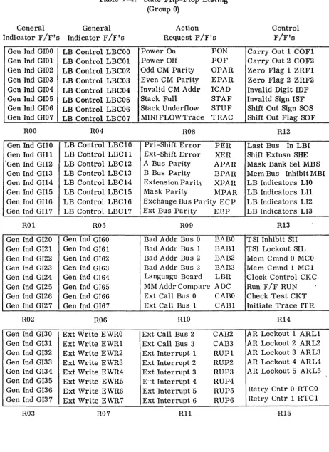
The Control Engine has a group of 256 addressable storage elements, called State flip-flaps, which perform mode control functions. In most cases, State flip-flops are actual binary storage elements. S0111e are general-purpose and are available for scratch-pad use. Others are dedicated and are controlled by internal and external events. The remainder are synthesized from outputs of various logical elen1ents in the processor and are called State pseudo-flip-flops. Table 1-4 is a Ii sting of MLP-900 State flip-flops. They are grouped by characteristics and the addressing structure of the MOVE mlnistep which can access them. Appendix C describes the indi vidual State flip-flops and their functions. Sonle general characteristics of the State flil)-flops are as follows:
• General Indicator nip-flops are not dedicated and may be used as scratch-pad regi s-ters for housekeeping and status data, program 11l0nitoring and testing.
• Language Board (LB) Control (LBCOO-15) flip-flops are available to use as lnode con-trol inputs to the OE and CE Language Boards. \Vhen they are not needed for this function, they may be used as general indicators.
• The External \Vri te (EWHO-7) group can be mechanized to provide signals to external devices, separately fronl the External Buses. \Vhen not dedicated, they can be used as general indicators.
• The Action Request (All) flip-flops respond to conditions which are to the lVILP-900 Processor what system interrupts are to a 111achine language processor. They allow the nornlal MINIFLO\V processing sequence to be modified by various internal con-ditions and external signals. \Vhen the hardware logic and the l\UNIFLO\V siInulta-neously attenlpt to set and reset one of these flip-flops, the set input will dOlninate. The complement of Action Requests and a sUlnnlary of their characteristics are described in paragraph 1. 4. 9.
• Control flip-flops are indicators which monitor status and control several important internal processor functions. When the hardware logic and the lVIINIFLOW simul-: taneously attempt to set and reset one of these flip-flops, the set input will dOlllinate.
Table 1-4. State Flip-Flop Listing (Group 0)
General General
Indicator F /F' s Indicator F /F' s
Gen Ind GIOO LB Control LBCOO Gen Ind GIOI LB Control LBCO 1 Gen Ind GI02 LB Control LBC02 Gen Ind GI03 LB Control LBC03 Gen Ind GI04 LB Control LBC04 Gen Ind GI05 LB Control LBC05 Gen Ind GI06 LB Control LBC06 Gen Ind GI07 LB Control LBCO 7
ROO H04
Gen Ind GIlO LB Control LBClO Gen Ind GIll LB Control LBCll 'Gen Ind GI12 LB Control LBC 12 Gen Ind GIl3 LB Control LBC 13 Gen Ind GI14 LB Control LBC14 Gen Ind GIl5 LB Control LBCI5 Gen Ind GI16 LB Control LBC16 Gen Ind G1I7 LB Control LBC17
ROI R05
Gen Ind GI20 Gen Ind GI60 Gen Ind GI2l Gen Ind GI61 Geu Ind GI22 Gen Ind G162 Gen Ind GI23 Gen Ind GI63 Gen Iud GI24 Gen Ind GI64 Gen Ind GI25 Gen Ind GI65 Gen Ind GI26 Gen Ind GI66 Geu Iud GI27 Gen Ind GI67
R02 R06
Gen Ind GI30 Ext Write EWRO Gen Ind GI3I Ext Write EWRI Geu Ind GI32 Ext Write EWR2 Gen Ind GI33 Ext \Vrite EWR3 Gen Ind GI34 Ext Write EWR4 Gen Ind GI35 Ext Write EWR5 Geu Iud GI36 Ext Write EWR6 Gen Ind GI37 Ext Write EWR 7
R03 R07
Action Request F/F's
Power On PON
Power Off POF
Odd CM Parity OPAR
Even CM Pari ty EPAR
Invalid CM Addr leAD
Stack Full STAF
Stack Underflow STUF
MINT FLOW Trace TH.AC
H08
Prj-Shift Error PEB.
Ext-Shift Error XER
A Bus Parity APAR
B Bus Parity BPAR
Extension Parity XPAH
Mask Parity l\1PAR
Exchange Bus Parity ECP
Ext Bus Parity EBP
H09
. Bad Adelr Dus 0 BADO Bad Adell' Bus 1 BAB1 Bad Adelr Bus 2 llAB2 Bad Aelelr Bus 3 BAll3
Language Board LllR
MM Adelr Con1pare ADC
Ext Call Bus 0 CABO
Ext Call Bus 1 CAB1
RIO
Ext Call Bus 2 CAB2
Ext Call Bus 3 CAll3
Ext Interrupt 1 RUP1
Ext Interrupt 2 RUP2
Ext Interrupt 3 RUP3
E-:t Interrupt 4 RUP4
Ext Interrupt 5 RUP5
Ext Interrupt 6 RUP6
Ril
Control F/F's
Carry Out 1 COFI Carry Out 2 COF2 Zero Flag 1 ZRFI Zero Flag 2 ZRF2 Invalid Digit IDF Invalid Sign ISF Shift Out Sign SOS
Sh ift aut Flag SO F
Rl2
Last Bus In LBI Shift Extnsn SHE Mask Bank Sel MBS McmBus InhibitMBI LB Indicators LIO LB Indicators LII LB Indicators LI2 LB Indicators LI3
R13
TSI Inhibit SII TSI Lockout SIL
MOlH Cmnd 0 MCO
Mem Cn1ncll MCI Clock Control CKC Run FIF RUN Check Test CKT Initiate Trace ITR
RI4
AR Lockout 1 ARLI AR Lockout 2 ARL2 AR Lockout 3 ARL3 AR Lockout 4 ARL4 AR Lockout 5 AHL5
Retry Cntr 0 RTCO Retry Cntr 1 RTC 1
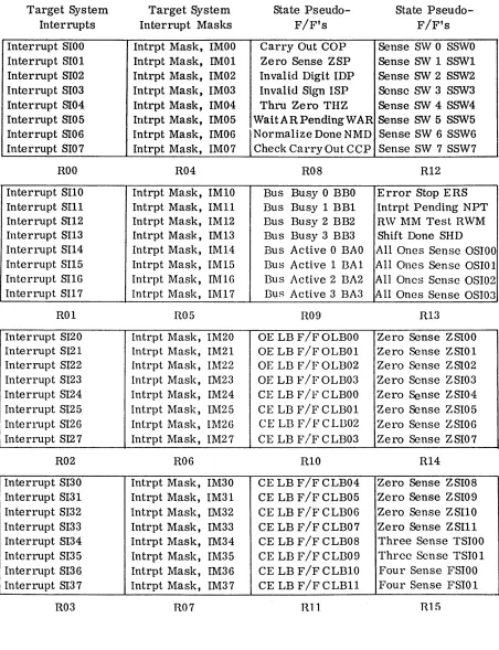
[image:31.615.101.564.95.731.2]Target System Interrupts Interrupt S100 Interrupt SI01 Interrupt S102 Interrupt SI03 Interrupt SI04 Interrupt SI05 Interrupt SI06 Interrupt SIO 7
ROO Interrupt SIlO Interrupt SIll Interrupt SI12 Interrupt SI13 Interrupt SIl4 Interrupt SIl5 Interrupt SI1G Interrupt SIl7 ROI Interrupt SI20 Interrupt SI2l Interrupt SI22 Interrupt SI23 Interrupt SI24 Interrupt SI25 Interrupt SI26 Interrupt SI27 R02 Interrupt S130 Interrupt SI3l Interrupt SI32 Interrupt 8133 Interrupt 8134 Interrupt 8135 Interrupt 8136 Interrupt SI37
R03
Table 1-4. State Flip-Flop Listing (continued) (Group 1)
Target System Interrupt Masks
Intrpt Mask, IMOO Intrpt Mask, IMOI Intrpt Mask, IM02 Intrpt Mask, IM03 Intrpt Mask, IM04 Intrpt Mask, IM05 Intrpt Mask, IM06 Intrpt Mask, IM07
R04
Intrpt Mask, IMlO Intrpt Mask, IMII Intrpt Mask, IM12 Intrpt Mask, IM13 Intrpt Mask, IM14 Intrpt Mask, IM15 Intrpt Mask, 11\116 Intrpt Mask, 11\'117
n05
Intrpt Mask, IM20 Intrpt 11ask, IM21 Intrpt 1\1ask, 11\1:22 Intrpt Mask, IM23 Intrpt Mask, IM24 Intrpt Mask, 11\'125 Intrpt Mask, 11\126 Intrpt Mask, IM27
R06
Intrpt Mask, IM30 Intrpt Mask, IM31 Intrpt Mask, IM32 Intrpt Mask, IM33 Intrpt Mask, IM34 Intrpt Mask, 11\135 Intrpt Mask, IM36 Intrpt Mask, IM37
R07
State Pseudo-F/F's
Carry Out COP Zero Sense ZSP In valid Digit IDP Invalid Sign ISP Thru Zero THZ WaitARPendingWAR Normalize Done NMD Check Carry Out CCP
R08
Bus Busy 0 BBO Bus Busy 1 BB1 Bus Busy 2 BB2 Bus Busy 3 BB3 Bus Active 0 BAO
DU8 Active 1 DA1
Bus Active 2 BA2 Dus Active 3 BA3
R09
OE LB F IF OLBOO OE LB F IF OLBOI OE LD F IF OLB02 OE LB F/F OLD03 CE LB 1"/1" C LBOO CE LB F/F CLBOI
CE LD FIfe' CLD02 CE LB F/F CLB03
R10
CE LB F/F CLB04 CE LB F IF CLB05 CE LB F/F CLB06 CELBF/FCLB07 CELBF/FCLB08 CELBF/FCLD09 CE LB F/FCLB10 CE LB F/F CLB11
Rll
State Pseudo-F/F's
Sense SW 0 SSWO Sense SW 1 SSW1 Sense SW 2 SSW2 Sense SW 3 SSW3 Sense SW 4 SSW4 Sense SW 5 SSW5 Sense SW 6 SSW6 Sense SW 7 SSW7
R12
Error Stop E RS Intrpt Pending NPT R\V l\lM Test RWM Shift Done SHD All Ones Sense OSIOO All Ones Sense OSI01 All Ones Sense OSI02 A 11 Ones Sense OSI03
R13
Zero Sense ZSIOO Zero Sense ZSIOI Zero Sense Z SI02 Zero Sense Z S103 Zero Sense ZSI04 Zero Sense ZS105 Zero Sense ZSIOG Zero Sense ZS107
R14
Zero Sense ZSI08 Zero Sense ZSI09 Zero Sense ZSI10 Zero Sense ZSI11 Three Sense TSIOO Three Sense TSIO 1 Four Sense FSIOO Four Sense FSIO 1
[image:32.612.104.556.130.719.2]• The last group of 64 State flip-flops are not hardware but pseudo .... flip-flops. These can be tested for either the true or complement condition but cannot be set and reset directly. A branch test on the first group of pseudo--flip-flops
(Group 1, R08) causes a "hiccup" (one clock delay) if the test fails.
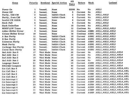
1. 4. 9 Action Request Servicing
There are 32 Action Request conditions in the MLP~900. The presence of an masked Target System Interrupt during a CE DE/WIN is also treated as an Action Request. Referring to Table 1-5, the first two Action Requests (AR's) provide a MINIFLOW entry for orderly start-up or shut-down when power is switched. The next five AR's (Priority 3-7) are set when high-priority errors or status conditions are detected in the Control Engine. Neglecting the Trace flip-flop, the next eight AR's function similarly for the Operating Engine. The four action requests labeled "Bad Addr" (Address) are set when an access is 11lade to l'vlain Memory and the bank addressed was not active in the system. This AR is also enabled if an I/O device is not presentwhen addressed. The Language BoardActionRequest (Priority 21) canbe used to indicate that a Main Menlory address was out of the range previously defined as a
boundary by opt