Super-Fast Low Power (SFLP) SRAM Cell for
Read/Write Operation
C.M.R. Prabhu
Faculty of Engineering and Technology Multimedia University, Melaka
Malaysia
Ajay Kumar Singh
Faculty of Engineering and Technology Multimedia University, Melaka
Malaysia
ABSTRACT
In this paper a Super-Fast Low-Power (SFLP) static random access memory (SRAM) cell has been proposed. The SFLP cell contains two tail transistors in the pull-down path of the respective inverter to minimize the write power consumption The cell is simulated in terms of speed, power and read stability. The simulated results show that the read and write power of the proposed cell is reduced up to 38% and 55% at 1.2 V respectively and cell achieves 2.2x higher read static noise margin (SNM) compared to the conventional 6T SRAM cell.
General Terms
SRAM, delay, power, write margin, threshold voltage, SNM..
Keywords
Static random access memory, PD-SOI, Write power, Write/read performance, Read SNM.
1. INTRODUCTION
Dueto requirement of light and portable devices, the demand high performance, low power digital very large scale integration (VLSI) system has increased [1-2]. In modern digital VLSI system, SRAM cell occupies a larger area on the chip. It is a great challenge to the researchers to restrict the power consumption in the modern processor due to demand of green technology. The power consumption of the systems can be reduced by reducing the power consumption of caches which occupies 60% to 70% of chip area. The power dissipated by caches is usually a major part of the total dissipated power. Due to this, design of power efficient high performance SRAM cell has gained importance. Various low power SRAM cell designs have been proposed [3-7]. Each design has its own merits and demerits. The cell stability is another important consideration for the cell designer [8,9]. In the present paper, a new Super-Fast Low-Power (SFLP) SRAM cell for read/write operation is proposed. The proposed cell is similar to the novel 8T SRAM cell except one extra transistor. This extra transistor is known as read access transistor, which is used to form the separate discharging path (read access transistor plus pull down transistor) during the read operation. Due to isolated read and write circuits, the read SNM of the proposed cell is enhanced. To avoid the any instability on the storage nodes in the unselected cells of the proposed 8T SRAM array, the switching behavior of the SFLP tail transistors are controlled by the respective storage nodes. During the write operation, the SFLP SRAM cell is similar to the Ref. [7] circuit which reduces the power consumption and reduces the write access time. The read operation is performed by only one bit line whereas write
operation is performed by two bit lines. Since, the discharging activity factor of the Super-Fast Low-Power (SFLP) cell is lower than the 6T cell, average read power consumption is 38% lower compared to the 6T SRAM cell. All the results are simulated in a CMOS 0.12µm technology using MICROWIND3 CAD tools [10]. The rest of the paper is organized as follows. In section 2, the operation of Super-Fast Low-Power (SFLP) cell is explained. Simulated results are discussed in section 3. Section 4 concludes the paper.
2. PROPOSED CIRCUIT DESCRIPTION
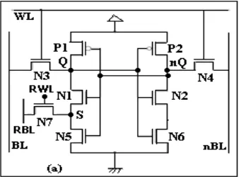
The complete schematic of the proposed Super-Fast Low-Power (SFLP) cell is shown in Fig. 1(a). The SFLP cell is divided into two circuits: write circuit and read circuit. The write circuit is similar to the 8T cell [7] and it is used to perform the write operation. The read operation is performed by two transistors (N7 and N5) which are used to perform the read operation. Transistor N7 is used to decouple the cell node from the read bit line during write operation/sleep mode. Due to this new design technique, the previously stored data remains intact in the cell during next write operation as long as RWL = 0. The layouts of the 6T and Super-Fast Low-Power (SFLP) SRAM cells, as shown in Fig. 1(b), are drawn in standard 0.12µm CMOS technology. The proposed SRAM cell has an area overhead of 11.7% due to additional two tail transistors. Because, the percentage of cell array to cache area is about 70%, the overall cache overhead is roughly (11.7% x70%) = 8.2% due to the proposed cell. The detail operation of the SFLP SRAM cell is:
[image:1.595.344.513.617.742.2]A read operation (RWL = 1, WL = 0) is performed by reading the data with help of the transistors N7 and N5. In read 1 operation, the transistor N5 is turned OFF, flips the node S to logic high, without allowing RBL to discharge which results lower power consumption. When node nQ stores data “1” (read 0 operation), transistor N5 turns ON. Now, the bitline (RBL) discharges through read access transistor N7 and pull down transistor N5. Since, storage nodes Q and nQ are completely isolated from bitlines during read operation; the voltage of the node which stores 0 is strictly maintained at the ground level.
3. SIMULATION RESULTS AND
DISCUSSIONS
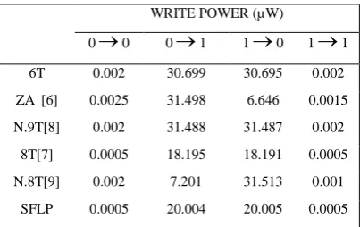
We have performed the simulation with help of BSIM4 model for 0.12 μm process technology. Threshold voltage of nMOS (pMOS) is set to 400mV. The 6T, Zero aware (ZA) [6], novel 9T (N.9T) [7], 8T [8], novel 8T (N.8T) [9] and SFLP cells are simulated and compared in terms of power consumption, access delay and current through each transistor. The simulated results are given in Tables (Table 1 –Table 7). In the proposed cell, overall power consumption is small compared to the 6T cell and other cells for 1→1 /0→0 write pattern. This is due to the no state transition and reduced sub-threshold current. Subthreshold leakage current is small (Table 7) due to the stack effect. Stacking of transistors is an effective way to reduce the subthreshold leakage current [4]. In 1→0/0→1 write pattern, power consumption is reduced due to no discharging activity at bitline (Table 1). The power dissipated in bitlines is only a part of the total cache power consumption due to increase in height of the proposed cell. The tag bitlines contribute only about 3% to the total cache power consumption during write operation [6]. The increased power consumption in wordline of the proposed cell during write mode can be compensated by equalizing the width of SFLP cell and the 6T cell layouts. The proposed cell height is longer than the 6T cell that increases the bitlines capacitace from 27.76 fF for the 6T cell to 32.51 fF for the proposed array with 128 cells per column in 0.12 μm technology. The total column write power consumption reduced by 71.31% in the SFLP cell for 0→0 and 1→1 write transitions where as 37.8% column power reduction is observed for 1→0 and 0→1 write patterns in the SFLP cell due to two tail transistors in the write circuit.
Fig 1: (b) Cell Layout
It is clear that the proposed SFLP SRAM cell consumes approximately 53.2% less average column write power (ACWP) than the conventional 6T SRAM cell. The 1→0/0→1 write transition speed of the proposed cell is faster than the conventional 6T cell and ZA cell (Table 1(a) &(b)), due to one OFF transistor in the pull down path of the inverter which lowers the discharging/charging time of bitlines. In the SFLP cell, a write operation can be performed for a minimum VWL value which is equal to the 0.56V instead of 0.81V as in the 6T cell (see Table 3). This indicates larger write margin of the proposed cell.
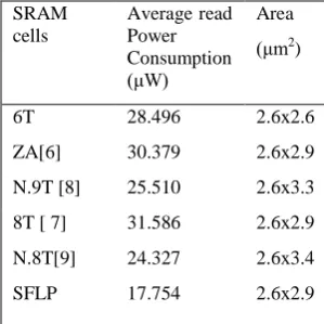
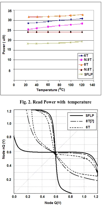
For read “1” operation (Q=1 & nQ=0), transistor N5 turned OFF and flips the node S to high. Due to no discharge at RBL considerable power is saved as seen in table 2. During read “0” operation, RBL discharges through two ON transistors N7 and N5. The average percentage read power reduction is 38% compared to the other cells (see Table 2). The read 1 access time is faster compared to the 6T cell (see Table 4). The read 0 delay is same compared to the conventional 6T cell. Table 7 gives the current flow through various transistors used in the 6T cell, 8T cell [7] and SFLP cell during read operation. Fig. 3 gives the variation of read power consumption with temperature for the 6-T cell and other cells. The proposed cell can be used up to T=120ºC with minimal power loss. This smaller change in power consumption is due to absence of leakage paths during read operation and due to isolation of write circuit from read circuit in SFLP cell. Due to isolation of read and write circuits, the read stability is enhanced and node Q is maintained strictly at 0V for nQ=Vdd (see Fig. 3)). The read SNM of the SFLP cell (420mV) is approximately 2.2xhigher than the SNM of the 6-T cell (195mV) and 1.3xlarger than the novel 8T cell [7] with a symmetrical butterfly curve. The use of low VTH (VTH=0.3V), transistors M7, M8 and M9 in the SFLP cell reduce the read SNM to 399mV compared to 110mV of novel 8-T cell. The SNM at different threshold voltages is given in Table 5. Due to increased change in current in current balance P1/N1 and P2/N2 at high temperature (T=120oC), read SNM decreases to 380mV from its room temperature value (Table 6). The percentage decrease in SNM temperature increases from 27oC to 120oC is only 9.5% in SFLP SRAM cell compared to 21% in novel 8T cell [7]. Fig. 2 gives the variation of read power consumption with temperature for the SFLP and the 6-T cells. The proposed cell can be used even in worse condition (T=120oC) with minimal power loss (10% in SFLP cell compared to 21% in novel 8T cell [7]). This smaller change in read power consumption is due to isolation of write circuit from read circuit in SFLP cell.
Table 1(a). Summary of write power for different input
WRITE POWER (µW)
0
0 0
1 1
0 1
16T 0.002 30.699 30.695 0.002
ZA [6] 0.0025 31.498 6.646 0.0015
N.9T[8] 0.002 31.488 31.487 0.002
8T[7] 0.0005 18.195 18.191 0.0005
N.8T[9] 0.002 7.201 31.513 0.001
[image:2.595.60.273.544.688.2] [image:2.595.328.530.595.722.2]Table 1(b). Summary of write Delay
WRITE DELAY(ps)
0
0 0
1 1
0 1
16T - 111 111 -
ZA [6] - 116 110 -
N.9T[8] 114 114
8T[7] 60 60
N.8T[9] - 121 117 -
SFLP - 62 62
[image:3.595.67.268.82.213.2]Table 2. Average read power and area
[image:3.595.348.487.96.230.2]Table 3.Access transistor (IN4) current
[image:3.595.93.243.256.406.2]Table 4. Read Delay
Table 5. SNM for different VTH
Table 6. SNM with different Temperature
SRAM cells
Average read Power Consumption (μW)
Area (μm2
)
6T 28.496 2.6x2.6
ZA[6] 30.379 2.6x2.9
N.9T [8] 25.510 2.6x3.3
8T [ 7] 31.586 2.6x2.9
N.8T[9] 24.327 2.6x3.4
SFLP 17.754 2.6x2.9
VWL
(volts)
IN4 in µA
6T ZA
[6]
8T
[7]
LPF
[9]
SFLP
1.2
1.0
0.81
0.63
0.62
0.60
0.58
98
98
96
-
-
-
-
75
74
71
61
57
-
-
75
73
71
60
58
-
-
75
73
71
60
58
-
-
76
74
70
61
59
58
56
SRAM cell Read Delay (ps) Read „0‟ Read „1‟
6T 80 80
ZA[6] 81 90
N. 9T[8] 94 94
8T [7] 90 90
N.8T[9] 85 14
SFLP 80 14
VTH SNM(mV)
6T ZA
[6] N.9T
[8] 8T
[7] N.8T
[9]
SFLP
0.3 - 106 352 110 359 399
0.4 195 155 390 165 397 420
0.7 - 398 433 405 443 465
Temp (oC)
SNM(mV) 6T ZA
[6] N.9T [8]
8T [7]
N.8T [9]
SFLP
-20 - 167 409 236 400 442
27 195 155 390 225 397 420
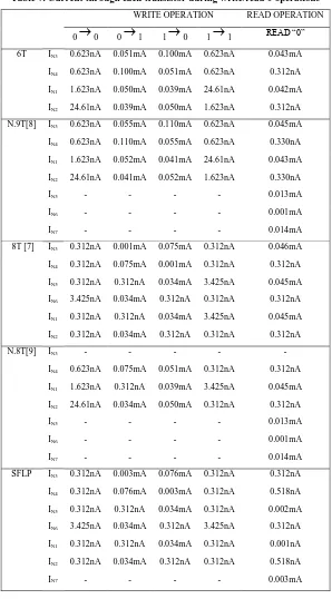
[image:3.595.314.513.444.547.2] [image:3.595.49.276.450.607.2]Table 7. Current through each transistor during write/read 0 operations
WRITE OPERATION READ OPERATION
0
0 0
1 1
0 1
1 READ “0”6T IN3 0.623nA 0.051mA 0.100mA 0.623nA 0.043mA
IN4 0.623nA 0.100mA 0.051mA 0.623nA 0.312nA
IN1 1.623nA 0.050mA 0.039mA 24.61nA 0.042mA
IN2 24.61nA 0.039mA 0.050mA 1.623nA 0.312nA
N.9T[8] IN3 0.623nA 0.055mA 0.110mA 0.623nA 0.045mA
IN4 0.623nA 0.110mA 0.055mA 0.623nA 0.330nA
IN1 1.623nA 0.052mA 0.041mA 24.61nA 0.043mA
IN2 24.61nA 0.041mA 0.052mA 1.623nA 0.330nA
IN5 - - - - 0.013mA
IN6 - - - - 0.001mA
IN7 - - - - 0.014mA
8T [7] IN3 0.312nA 0.001mA 0.075mA 0.312nA 0.046mA
IN4 0.312nA 0.075mA 0.001mA 0.312nA 0.312nA
IN5 0.312nA 0.312nA 0.034mA 3.425nA 0.045mA
IN6 3.425nA 0.034mA 0.312nA 0.312nA 0.312nA
IN1 0.312nA 0.312nA 0.034mA 3.425nA 0.045mA
IN2 0.312nA 0.034mA 0.312nA 0.312nA 0.312nA
N.8T[9] IN3 - - - - -
IN4 0.623nA 0.075mA 0.051mA 0.312nA 0.312nA
IN1 1.623nA 0.312nA 0.039mA 3.425nA 0.045mA
IN2 24.61nA 0.034mA 0.050mA 0.312nA 0.312nA
IN5 - - - - 0.013mA
IN6 - - - - 0.001mA
IN7 - - - - 0.014mA
SFLP IN3 0.312nA 0.003mA 0.076mA 0.312nA 0.312nA
IN4 0.312nA 0.076mA 0.003mA 0.312nA 0.518nA
IN5 0.312nA 0.312nA 0.034mA 0.312nA 0.002mA
IN6 3.425nA 0.034mA 0.312nA 3.425nA 0.312nA
IN1 0.312nA 0.312nA 0.034mA 0.312nA 0.001nA
IN2 0.312nA 0.034mA 0.312nA 0.312nA 0.518nA
Fig. 2. Read Power with temperature
Fig. 3.Graphical representation of SNM
4. CONCLUSION
In the proposed cell, the power saves up to 55% during write operation and 38% during read operation compared to the 6T cell. The average column write power reduces in the SFLP SRAM cell. The SNM of the proposed SFLP cell is 2.2x higher than the 6-T cell and 1.3x the novel 8T cell. The SFLP cell and be used in worse condition (T = 120oC) with minimal power loss and stability loss.
5. REFERENCES
[1] N.S. Kim, D. Blaauw, T. Mudge, “Quantitative analysis and opti- mization techniques for on-chip cache leakage power,” IEEE Trans. Very Large Scale Integr. (VLSI) Syst., vol. 13, no. 10, pp. 1147-1156, Oct. 2005. [2] M. Yamaoka, R. Tsuchiya, and T. Kawahara, “SRAM
circuit with ex- panded operating margin and reduced stand-by leakage current using Thin-BOX FD-SOI transistors,” IEEE J. Solid-State Circuits, vol. 41, no. 11, pp. 2366-2372, Nov. 2006.
[3] S. Inaba, H. Nagano, K. Miyano, I. Mizuushima, Y. Okayama, T. Nakauchi, K. Ishimaru, and H. Ishiuchi, “ Low-power logic circuit and SRAM cell applications with silicon on depletion layer CMOS (SODEL CMOS) technology,” IEEE J. Solid-State Circuits, vol. 41, no. 6, pp. 1455-1462, June 2006.
[4] A. Chandrakasan, W. J. Bowbill and F. Fox, “Design of High Perfor- mance Microprocessor Circuits,” Wiley-IEEE Press, p. 584, 2000.
[5] E. Grossar, M. Stucchi, K. Maex, and W. Dehaene, “Read stability and write-ability analysis of SRAM cells for nanometer technologies,” IEEE J. Solid-State Circuits, vol. 41, no. 11, pp. 2577-2588, Nov. 2006.
[6] Y. Chang, F. Lai, and C. Yang, “Zero-aware asymmetric SRAM cell for reducing cache power in writing zero,” IEEE Trans. Very Large Scale Integr. (VLSI) Syst., vol. 12, no. 8, pp. 827-836, Aug. 2004. [7] C.M.R. Prabhu and A.K. Singh, Novel Eight-Transistor
SRAM cell for Write Power reduction,” IEICE Electron. Express, vol.7, no. 16, pp. 1175-1181, 2010.
[8] Z. Liu and V. Kursun, “Characterization of a Novel Nine-Transistor SRAM cell,” IEEE Trans. Very Large Scale Integr. (VLSI) Syst., vol. 16, no. 4, pp. 488-492, Aug. 2008.
[9] A. Sil, S. Ghosh, and M. Bayoumi, “A Novel 8T SRAM Cell with improved Read-SNM,” Circuits and Systems, 2007, NEWCAS 2007. IEEE Northeast Workshop, vol. 5-8, pp 1289-1292, Aug. 2007.