Abstract—We propose a wide angle, efficient and low loss 1 3 power splitter based on triangular lattice air holes silicon slab Pho-tonic Crystal (PhC). Desired power splitting ratio was achieved by altering the structure at the junction area of the power splitter. Simulation results obtained using 2-Dfinite difference time domain method show that for TE polarization incident signal, the power is distributed almost equally with total normalized transmission of 99.74% and negligible reflection loss at the 1550 nm optical op-erating wavelength. In addition, the power splitter can operate at 1388 nm and 1470 nm optical wavelengths.
Index Terms—Finite difference method, optical devices, optical tuning, photonic crystal.
I. INTRODUCTION
P
HOTONIC CRYSTAL (PhC) is a low loss structure which the refractive index of its different materials alternates pe-riodically. PhC devices work based on both bandgap theory for guiding light in one direction, and total internal reflection to confine light in the other direction. Using the two mechanisms, the scattering loss induced by wall roughness in conventional planar waveguides [1] can be minimized. In addition, successful signal propagation through 90 degree sharp bend or any degree of bending in PhC was shown both theoretically and experimen-tally [2]–[4].In general, there are two types of PhC slabs. Thefirst is di-electric rods in air, which shows a transverse magnetic (TM) bandgap, and the second is air holes in dielectric slab that ex-hibits transverse electric (TE) bandgap [5]. In terms of fabrica-tion difficulty, air hole slab is much easier to fabricate and is more reliable for practical applications. PhC devices fabricated by dielectric rods in air, in contrast, induce more out of plane
Manuscript received December 04, 2011; revised May 14, 2012; accepted June 04, 2012. Date of publication June 20, 2012; date of current version August 17, 2012. The work was supported in part by MOHE High Impact Research under Grant A000007-50001.
D. C. Tee, S. R. Sandoghchi, and F. R. Mahamd Adikan are with the Photonics Research Group, Department of Electrical Engineering, University of Malaya, 50603 Kuala Lumpur, Malaysia (e-mail: [email protected]; [email protected]; [email protected]).
T. Kambayashi is with the Department of Electrical Engineering, Nagaoka University of Technology, Niigata 940-2188, Japan (e-mail: [email protected]).
N. Tamchek is with the Department of Physics, University Putra Malaysia, 43400 Serdang, Selangor, Malaysia (e-mail: [email protected]).
Color versions of one or more of thefigures in this paper are available online at http://ieeexplore.ieee.org.
Digital Object Identifier 10.1109/JLT.2012.2205369
losses due to the insufficient vertical confinement by total in-ternal reflection. Some researchers apply high-index segments in the dielectric rods leading to vertical confinement, resulting in extremely low out of plane losses in the PhC waveguides [6]. However, this adds to fabrication complexity.
PhC has emerged as an important enabling key for fu-ture compact optical integrated devices. They include basic optical components such as power splitters [7], directional couplers [8], and optical filters [9]. Theoretically, PhC based components should have nearly zero reflection and 100% trans-mission. However, practical devices are limited by fabrication accuracies.
PhC slab based 1 2 power splitter, or Y-branch power di-vider, has been demonstrated and fabricated by many research groups since a decade ago [4], [7], [10]–[13]. However, recently, there have been growing interests in 1 3 PhC power splitters, enabling triple play capabilities for example. By applying mul-timode interference (MMI) technique [14], or coupling [15], [16], researchers have been able to demonstrate 1 3 power splitter theoretically and experimentally. In the work reported by Zhanget al.[14], the optimum normalized transmittance cal-culated through simulation is around dB for each branch at 1567.4 nm wavelength and the experimental results show values around dB for each branch at 1550 nm. Such a high trans-mission loss is not desirable for efficient photonic integrated devices. Another problem for MMI devices is the considerable small output splitting angle which limits its application. In a sep-arate work, a power splitter based on dielectric rod in air was fabricated by Liu [15], which shows the transmission loss of 10%. However, the device is not suitable for optical communi-cation because of its operating wavelength in the visible range (532 nm). In another attempt, a 1 3 power divider based on ring resonators and directional couplers has been reported by Djavidet al.[16] which shows 99% transmission. Using dielec-tric rods in air, they obtained about 33% normalized transmis-sion for each of the three branches at operating wavelength of 1594 nm through the coupling between the waveguide and the ring resonators. In relation to this coupling technique, the size of the PhC will become longer due to the required interaction length for complete transfer of the propagating electromagnetic wave from one waveguide to another. Therefore, such a design may not fulfill the high integration requirement for compact op-tical integrated devices.
Beside the aforementioned MMI and coupling methods, modification of PhC structure can result in 1 3 power split-ters. In this manuscript, a structure tuning method for a 1 3
Fig. 1. Basic 1 3 power splitter. Zoom-in box shows the modified power splitter with drop holes DH1 and DH2 at the junction area.
PhC slab based power splitter is proposed and the results are verified by numerical simulation. This paper is organized as follows. Section II describes the design and parameters used for the proposed splitter. In Section III, the simulation results and discussion are presented. And finally, conclusion and future works are presented in Section IV.
II. DESIGN ANDPARAMETERS
A basic PhC slab based power splitter with triangular lattice air holes is shown in Fig. 1. It consists of a Y branch with 120 degree angle and a waveguide connected at the junction. Gen-erally, the waveguides are similar, and the signal is input from the position indicated in Fig. 1. The output power for each of the branches are measured at the locations shown in the samefigure, where P1, P2, and P3 are the transmission powers at the upper, middle, and lower output branches respectively. Moreover, the reflection loss, , is measured at half lattice distance before the input signal excitation location, and , is the measure of total input power, indicating the amount of power entered into the structure and distributed within it [14].
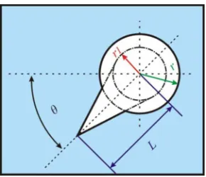
The modified power splitter is shown in the zoom-in box in Fig. 1 where the design has been changed at the junction area of the branches by including two drop holes (DH1 and DH2). The layout of the drop hole is shown in Fig. 2. The drop holes are designed to interact with the incoming electromagnetic wave while they reduce the reflection loss and guide the wave into the branches effectively [13]. The main parameters of the drop hole are , and , where is the radius of the drop hole, is the length from center of drop hole to the sharp corner, and is the bending angle, with positive for upward bending and negative for downward. In the layout shown in Fig. 2, r indicates air hole radius. In the simulation, DH1 is bent downward and DH2 is bent upward , which means that the two drop holes are approaching each other or crossing each other depending on the degree of bending and the drop hole’s length. Any changes in and will either affect the reflection loss or power splitting ratio or both at the same time.
[image:2.592.59.266.62.223.2]In this work, a 2-D finite difference time domain (FDTD) method has been used for analyzing the proposed device. For the simulation, the effective refractive index of the PhC slab
Fig. 2. Layout of the drop hole used in the 1 3 power splitter.
with holes is calculated using the effective index method [17]. Moreover, air hole radius of nm, lattice constant of
nm, and slab-effective refractive index of 2.9 corresponding to 240 nm thick silicon on silica substrate operating at 1550 nm wavelength are used [8]. The aforementioned effective index is applicable for other wavelengths as well [8]. As 2-D method is used in the simulation, the out of plane losses are fully ignored. Detailed study showed that the magnitude of these losses is very low [18].
The PhC slab is on the x-y plane, with the z axis pointing out of plane. The input signal propagates along the x-axis. The 2-D FDTD mesh size used in this simulation are
nm. The time step, is obtained from Courant limit and is equal to seconds. We have used 200 000 iterations for the FDTD computation to obtain the steady-state result. The overall size of splitter is about 13 um 10 um, and it can be fur-ther reduced because the structure is only altered at the junction area. Its small size makes it promising for the future compact photonic integrated optical devices.
A finite computation region with general Neumann or Dirichlet boundary conditions causes the propagating elec-tromagnetic wave to be reflected back at the boundary of computational region. Therefore, a 22 layer Berenger perfectly match layer (PML) [19] is applied at the boundary regions to absorb the entire outward propagating electromagnetic wave. TE polarization has been used for the simulation with its mag-neticfield only in the z direction , and, the electricfield in both x and y directions ( and ).
III. RESULT ANDDISCUSSION
To evaluate the advantages of the proposed structure, the basic power splitter without drop holes is simulated and com-pared with the proposed splitter using the aforementioned parameters.
Fig. 3. Basic power splitter design. Normalized output transmission and refl ec-tion powers are shown at the top left corner in thefigure. The inset shows the contour plot at the junction area.
into multimode. The mono-mode branches thus experience mis-match with the incoming multimode electromagnetic wave and therefore, a considerable portion of power is lost due to refl ec-tion and dispersion.
In the proposed design, drop holes are utilized to reduce the waveguide space at the junction area and consequently to pre-vent the multimode propagation and mismatch from occurring. Besides, parameters of the drop holes, can alter and match the impedance of waveguides, and consequently result in equal dis-tribution of the incoming mode wave into three single-mode waves propagating in the branches.
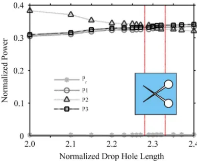
[image:3.592.55.275.63.241.2]Palamaru et al. [20] showed that a tiny hole, followed by a line of holes in a gradually increasing size manner, could adiabatically convert conventional waveguide mode into a PhC waveguide mode to achieve mode matching without incurring significant loss. The concept is verified experimentally by Wilson et al. [13]. Besides, impedance matching between output channels and input channel reduces the reflected wave and increases the power transmission efficiency. By adding extra holes to the input channel, intrinsic impedance can be tuned to achieve almost perfect impedance matching [21]. In order to split the power equally among the output channels with very low reflection, the branches’ impedance should be similar and should match with input channel [21]. Optimization for the splitter is done by tuning one of the parameters while the other two arefixed. Repeating the procedure for other parameters (if required) can disclose a local optimized region. First, the radius of the drop, , and the bending angles, and arefixed, while the effect of drop’s length is studied. The result shown in Fig. 4 indicates that for the length size within 2.2 to 2.4 , the normalized output transmission is divided equally on each output port, with the optimum length occurring at . Further optimizations were not necessary. The layout for the drop hole length at is shown in the inset. With the current technology, fabrication of holes with accuracy up to 15 nm has been achieved using focused ion beam method [22]. The smallest dimension in the drop hole which is equal to the mesh size used in this simulation is 10 nm which will be viable
Fig. 4. Normalized output transmission and reflection power versus drop hole
length normalized with respect to lattice constant at and
. The interval between the vertical red lines indicates the optimum operation region. The optimum region is calculated based on the computation accuracy of the simulation. The inset shows the layout of the drop holes at
.
Fig. 5. Steady-state magneticfield distribution at
and at 1550 nm wavelength. The inset shows the contour plot at the
junction area.
with a slight improvement in the aforementioned fabrication technology.
Steady-state magneticfield distribution at point , and is shown in Fig. 5 indicating a desirable field separation into the branches. The multimode behavior at the junction area has been suppressed by the drops showing a good impedance matching between channels, leading to a considerable reduction in reflection and dispersion loss. The normalized transmitted power at P1 is 32.93%, at P2 is 33.26%, and at P3 is 33.53%, while the reflection loss is as low as 0.26%, which is quite negligible. The slight asymmetry in output power P1 and P3 is due to the possibility that the discretization mesh used in the simulation do not share the central axis of symmetry with the structure. Therefore, there is a 0.6% of tolerance in the calculated output powers. This suggests an interval (a region) of optimum operation highlighted in Fig. 4. Within the interval, the normalized power transmission is nearly 33% for all output
branches. For , and the
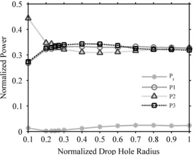
[image:3.592.321.535.302.471.2]Fig. 6. Normalized output transmission and reflection power versus drop hole
radius , normalized with respect to air hole radius , at and
.
the work reported in [14], our design shows better performance for power transmission at 1550 nm.
The parameters of drop holes within the local optimum op-erating region are feasible for fabrication. From the results, the drop hole length for the proposed slab can be varied between 1003 nm and 1025 nm. In order to show theflexibility of the fabrication parameters for the proposed splitter, the sensitivity of the design to the other parameters are studied, as follows.
While the drop’s length at and bending angles at arefixed, the drop’s radius, , is changed. The result, shown in Fig. 6, indicates that while radius is changing from to , the average reflection is negligible, and is about 0.33%, while the normalized output transmission is almost equal for all branches. This allows for a % toler-ance in drop’s radius for fabrication of the drop holes. The ef-fect of drop’s radius in reflection loss is explained by waveguide input impedance that is altered by drop’s parameters. Increase in drop’s radius decreases the local effective index experienced by the incoming electromagnetic wave and thus increases the impedance mismatch. Therefore, more light is reflected back toward the input direction and consequently reflection loss in-creases. In contrast, as reduces , DH1 and DH2 be-come smaller in size, and the device starts to behave like the basic power splitter as shown in Fig. 1, with most of the output signal intensityflowing into the direction of P2.
Study of the bending angles shows that, while the drop’s length isfixed at and drop’s radius at , for the bending degree from to , the nor-malized output transmission for each branch is within % % with low reflection. This is depicted in Fig. 7. Also, this toler-ance in bending angle, , adds extra advantage in fabrication of drop holes and thus the splitter. Fig. 8 shows thefield distribu-tion at bending angles of 25 , 35 and 45 . Fig. 8(a) represents thefields amplitude for the corresponding yellow dash-dot line in Fig. 8(b). It shows that the magneticfield is continuous, while electricfield and power are discontinuous across the drop hole (low index region). This discontinuity is due to the fact that the electric displacementfield requires to be continuous across the index contrast interface. Light confinement in low index mate-rial region of sub-wavelength size can be achieved by the
dis-Fig. 7. Normalized output transmission and reflection power versus bending
angle at and .
Fig. 8. Field distribution for different bending angles. (a) Field amplitude cor-responding to the dash-dot line (yellow) in (b), where P is the power, Ey is the y-component of the electricfield vector and Hz is z-component of the magnetic field vector. Power distribution (b) at bending angle of 25 , (c) at bending angle of 35 , and (d) at bending angle of 45 .
continuity of electricfield perpendicular to the index contrast interface. The confinement of light power in the drop holes, as shown in Fig. 8(b)–(d), is due to both Ey and Ex distributions. Naturally, larger Ey values correspond to a larger transmittance into the center branch and Ex to the upper and lower branches. By introducing drop holes, the Ey and Ex distribution is altered and simulation result indicates that at certain range of drop’s bending angles, the transmitted powers to the branches are sim-ilar. This is possibly due to the fact that, within the aforemen-tioned bending range, the power is trapped and guided in the drop holes, and distributes equally to all branches. In contrast, more powerflows into the P2 direction as the bending angle is outside of the range mentioned above. This possibly can de-scribe the impedance matching caused by altering the bending angle.
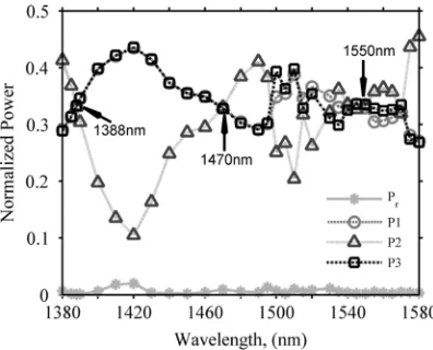
[image:4.592.66.262.63.220.2] [image:4.592.315.540.263.423.2]Fig. 9. Normalized output transmission and reflection power versus
[image:5.592.59.272.268.437.2]wave-length at and .
Fig. 10. Steady-state magneticfield distribution for
and at 1388 nm wavelength. The inset shows the contour plot
at the junction area.
Fig. 11. Steady-state magneticfield distribution for
and at 1470 nm wavelength. The inset shows the contour plot
at the junction area.
we can operate the splitter at three different optical commu-nication spectrums to suit certain applications. This multiple operating wavelengths feature has not been reported before.
wide range of wavelengths. However, different wavelengths may experience different transmittance. In the proposed splitter, similar transmittance has been demonstrated for 1388 nm and 1470 nm wavelengths in addition to 1550 nm, opening the potential for triple play applications.
IV. CONCLUSION
In this study, a power splitter was proposed by modifying the lattice structure in which two drop holes were introduced at the junction. Based on the results, the structure is capable of di-viding the electromagnetic wave power desirably, i.e., % at each branch with a very negligible reflection loss, at operating wavelength of 1550 nm. Besides, it was shown that this splitter is capable of operating at two other important optical communi-cation bands, E-band and S-band, with desirable power splitting ratio and low reflection loss.
ACKNOWLEDGMENT
The authors would like to thank K. Matsunaga for his tech-nical help.
REFERENCES
[1] J. M. Elson, “Propagation in planar waveguides and the effects of wall roughness,”Opt. Exp., vol. 9, pp. 461–475, 2001.
[2] A. Chutinan and S. Noda, “Waveguides and waveguide bends in two-dimensional photonic crystal slabs,”Phys. Rev. B, vol. 62, pp. 4488–4492, 2000.
[3] S. Olivier, H. Benisty, M. Rattier, C. Weisbuch, M. Qiu, A. Karlsson, C. J. M. Smith, R. Houdre, and U. Oesterie, “Resonant and nonresonant transmission through waveguide bends in a planar photonic crystal,”
Appl. Phys. Lett., vol. 79, pp. 2514–2516, 2001.
[4] S. Foghani, H. Kaatuzian, and M. Danaie, “Simulation and design of a wideband T-shaped photonic crystal splitter,”Optica Applicata, vol. XL, pp. 865–872, 2010.
[5] S. G. Johnson, P. R. Villeneuve, S. Fan, and J. D. Joannopoulos, “Linear waveguides in photonic-crystal slabs,”Phys. Rev. B, vol. 62, pp. 8212–8222, 2000.
[6] A. A. M. Kok, J. J. G. M. van der Tol, R. Baets, and M. K. Smit, “Reduc-tion of propaga“Reduc-tion loss in pillar-based photonic crystal waveguides,”
J. Lightw. Technol., vol. 27, no. 17, pp. 3904–3911, Sep. 2009. [7] N. Nozhat and N. Granpayeh, “Analysis and simulation of a photonic
crystal power divider,”J. Appl. Sci., vol. 7, pp. 3576–3579, 2007. [8] I. Park, H. S. Lee, H. J. Kim, K. M. Moon, S. G. Lee, B. H. O. S. G. Park,
and E. H. Lee, “Photonic crystal power-splitter based on directional coupling,”Opt. Exp., vol. 12, pp. 3599–3604, 2004.
[9] Z. Zhang, M. Dainese, L. Wosinski, S. Xiao, M. Qiu, M. Swillo, and U. Anderson, “Opticalfilter based on two-dimensional photonic crystal surface-mode cavity in amorphous silicon-on-silica structure,”Appl. Phys. Lett., vol. 90, pp. 041108–041110, 2007.
[10] L. J. Kauppinen, T. J. Pinkert, H. J. W. M. Hoekstra, and R. M. de Ridder, “Photonic crystal cavity-based Y splitter for mechano-optical switching,”IEEE Photon. Technol. Lett., vol. 22, no. 13, pp. 966–968, Jul. 2010.
[image:5.592.59.272.492.661.2][12] L. H. Frandsen, P. L. Borel, Y. X. Zhuang, A. Harpoth, M. Thorhauge, M. Kristensen, W. Bogaerts, P. Dumon, R. Baets, V. Wiaux, J. Wouters, and S. Beckx, “Ultralow-loss 3-dB photonic crystal wave-guide splitter,”Opt. Lett., vol. 29, pp. 1623–1625, 2004.
[13] R. Wilson, T. J. Karle, L. Moerman, and T. F. Krauss, “Efficient photonic crystal Y-junctions,”J. Opt. A, Pure Appl. Opt., vol. 5, pp. S76–S80, 2003.
[14] M. Zhang, R. Malureanu, A. C. Kruger, and M. Kristensen, “1 3
beam splitter for TE polarization based on self-imaging phenomena in photonic crystal waveguides,”Opt. Exp., vol. 18, pp. 14944–14949, 2010.
[15] C. Y. Liu, “Fabrication and optical characteristics of silicon-based two-dimensional wavelength division multiplexing splitter with photonic crystal directional waveguide couplers,”Phys. Lett. A, vol. 375, pp. 2754–2758, 2011.
[16] M. Djavid, A. Ghaffari, F. Monifi, and M. S. Abrishamian, “Photonic crystal power dividers using L-shaped bend based on ring resonators,”
J. Opt. Soc. Amer. B, vol. 25, pp. 1231–1235, 2008.
[17] O. V. Ivanova, R. Stoffer, L. J. Kauppinen, and M. Hammer, “Varia-tional effective index method for 3-D vectorial scattering problems in photonics: TE polarization,” inProc. PIERS, Moscow, Aug. 2009, pp. 1038–1042.
[18] G. R. Hadley, “Out-of-plane losses of line-defect photonic crystal waveguides,”IEEE Photon. Technol. Lett., vol. 14, no. 5, pp. 642–644, May 2002.
[19] J. P. Berenger, “A perfectly matched layer for the absorption of elec-tromagnetic waves,”J. Computational Phys., vol. 114, pp. 185–200, 1994.
[20] M. Palamaru and Ph. Lalanne, “Photonic crystal waveguides: Out-of-plane losses and adiabatic modal conversion,”Appl. Phys. Lett., vol. 78, pp. 1466–1468, 2001.
[21] S. Boscolo, M. Midrio, and T. F. Krauss, “Y junctions in photonic crystal channel waveguides: High transmission and impedance matching,”Opt. Lett., vol. 27, pp. 1001–1003, 2002.
[22] Y. Kurokawa, Y. Ohno, S. Kishimoto, T. Okazaki, H. Shinohara, and T. Mizutani, “Fabrication technique for carbon nanotube single-electron transistors using focused ion beam,”Jpn. J. Appl. Phys., vol. 43, pp. 5669–5670, 2004.
Din Chai Teereceived the B.S. degree (withfirst-class honors) in telecommu-nication engineering from the University of Malaya, Kuala Lumpur, Malaysia, in 2010, where he is currently working toward the Ph.D. degree.
In 2010, he was selected to represent the University of Malaya to participant JENESYS (Japan-East Asia Network of Exchange for Students and Youths) ex-change program at Nagaoka University of Technology, Niigata, Japan. He is currently a Research Assistant with the Flat Fibre Laboratory, Department of Electrical Engineering, University of Malaya, Kuala Lumpur, Malayasia. His current research interests include simulation on photonic crystal slab based de-vices, photonic crystalfiber, and development of novel Flat Fiber applications.
Toshio Kambayashireceived the Ph.D. degree from the Tokyo Institute of Technology, Tokyo, Japan, in 1977.
He is currently a Professor with the Department of Electrical Engineering, Nagaoka University of Technology, Niigata, Japan, and is involved in research on optical waveguides, optical integrated circuits, and photonic crystal devices. From 1977 to 1979, he was a Lecturer with the Research Laboratory of Preci-sion Machinery and Electronics, Tokyo Institute of Technology, where he was involved in the research of monolithically semiconductor laser fabrication for integrated optical circuits. He joined the Nagaoka University of Technology in 1979 as an Associate Professor. From 1981 to 1983, he was a Research Officer at the University of Bath, Bath, U.K., where his work involved the research of semiconductor lasers and LED’s for integrated optical circuits.
Dr. Kambayashi is a member of the Institute of Electronics and Communica-tion Engineers of Japan and the Japan Society of Applied Physics.
Seyed Reza Sandogchireceived the B.S. degree (withfirst-class honors) in telecommunication engineering from the Sadjad Institute of Higher Education, Mashhad, Iran, in 2005, and the M.S. degree in telecommunication from Univer-sity of Malaya, Kuala Lumpur, Malaysia, in 2011. His dissertation investigated the refractive index profile characterization methods.
His research mainly includes modeling and simulation of optical devices and developing characterization systems. He has been involved in establishment of fiber drawing facilities in University of Malaya, Kuala Lumpur, Malaysia, where he is currently working with the opticalfiber fabrication team at the Flat Fibre Lab.
Nizam Tamchekreceived the B.S. degree in physics from Kanazawa Univer-sity, Japan, in 2001, and the M.Sc. and Ph.D. degrees in photonics from the University of Malaya, Kuala Lumpur, Malaysia, in 2010.
He is currently a Lecturer with the Department of Physics, University Putra Malaysia. He joined the MCVD Laboratory at Telekom Research and Devel-opment in 2009. His work has focused on understanding the photonics device fabrication using FHD and MCVD system and development of photonics de-vice for telecommunication and sensors.
Faisal Rafiq Mahamd Adikanreceived the Ph.D. degree from the Optoelec-tronics Research Centre, University of Southampton, Southampton, U.K., in 2007.
His Ph.D. work onflatfibre produced an international patent. He is currently the Head of the Photonics Research Group, University of Malaya, Kuala Lumpur, Malaysia, where he is involved with developing novel fabrication process to incorporate optically active materials into a glass matrix. He spe-cializes in glass-based integrated optical devices for use in telecommunication and sensing applications. He has authored and coauthored more than 70 journal and conference papers on optics and engineering education.