http://dx.doi.org/10.4236/cs.2016.71004
CFOA Based Band Pass and Band Stop
Ladder Filter—A New Configuration
Praween K. Sinha, Neelam Sharma, Simran Agarwal, Sudipto Saha
Electronics and Communication Department, Maharaja Agrasen Institute of Technology, New Delhi, India
Received 13 November 2015; accepted 18 January 2016; published 21 January 2016
Copyright © 2016 by authors and Scientific Research Publishing Inc.
This work is licensed under the Creative Commons Attribution International License (CC BY). http://creativecommons.org/licenses/by/4.0/
Abstract
A new technique for the conversion of ladder based filter into CFOA based filter has been proposed. The technique uses signal flow graph and converts the existing LC ladder based filter into band pass & band stop configurations. The design of band pass and band stop filter has been realized using the proposed technique. The proposed configuration is implemented using CFOA as an ac-tive device and all the capacitors are grounded. CFOA based circuits have greater linearity, high dynamic rate, high slew rate and high signal bandwidth. Simulation has been carried out using simulation software P Spice (v10.1). The simulation results have been demonstrated and discussed.
Keywords
CFOA-Current Feedback Operational Amplifier, Ladder Filter, Signal Flow Graph, Current Mode, Voltage Mode, Band Pass Filter, Band Stop Filter
1. Introduction
The birth of electronics lead to the need of new active devices and invention of transistors was extremely bene-ficial. After that VFA’s or Voltage Feedback Operational Amplifiers were developed. However their dynamic performances were limited because of the gain bandwidth product and slew rate. Hence nowadays there is an in-clination towards current mode circuits. The advantages of current mode circuits over voltage mode circuits are higher signal bandwidth, larger dynamic range, low-voltage operation, greater linearity, lower power consump-tion, simpler circuitry and simple implementation of signal operations, such as addition and subtraction [1]-[3].
large number of OTA’s. This paper presents a systematic approach using signal flow graph technique for realiz-ing the passive ladder based band pass and band reject filter into CFOA based band pass and band reject filter. The resulting filters requires CFOA, resistors and capacitors and most of the capacitors are grounded. Further-more, for thin film fabrication the use of grounded capacitors eliminates the etching process and reduces the number of gold contacts. Hence leading to a greater circuit reliability.
Current feedback operational amplifier (CFOA) based CM circuits have received considerable attention in many filtering and signal processing applications. Symbol diagram of the CFOA is shown in Figure 1. With the help of CFOA we can achieve the same characteristics of ladder based filter as they were in the original circuit and excluding the inductors [4]-[6]. Moreover, CFOA provides faster response and can operate at high fre-quency at high gain.
Although there has been a lot of activity on Universal Voltage Mode & Current Mode biquad filters realisa-tion using CFOA’s, comparatively only a few researchers have explored the methods of designing higher order filters using CFOA’s. Previously, Rathore and Khot [7] have designed a Low Pass and High Pass filter configu-ration using CFOA. They have given a systematic method of deriving CFOA based all grounded capacitor filter from Current Mode RLC prototype ladders. Sinhaetl proposed a Signal Flow Graph approach for realizing CFOA based high pass and low pass ladder filter [8]. Referring to the Low Pass and High Pass configurations presented in research paper [7][8], we have prepared two different combinations of Band Pass and Band Reject Filter.
In this paper, active realization of Band Pass and Band Reject ladder filter using current feedback operational amplifier (CFOA) has been presented. We have considered two cases in both band pass and band reject filters and obtained the result of both the cases.
The paper is organised as follows: 1) Introduction.
2) Transformation of passive ladder based band pass filter into CFOA based band pass filter(Circuit Analysis of ladder based filter using KVL & KCL, Signal Flow Graph, Equivalent CFOA based Circuit and Output Waveforms).
3) Transformation of passive ladder based bandreject filter into CFOA based bandreject filter(Circuit Analysis of ladder based filter using KVL & KCL, Signal Flow Graph, Equivalent CFOA based Circuit and Output Waveforms).
4) Simulation Results. 5) Conclusion.
2. Transformation of Ladder Band Pass Filter into CFOA Based Band Pass Filter
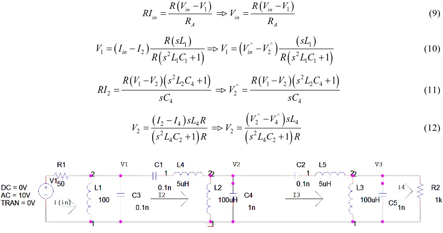
Improvements have been done in the passive ladder based Band pass filter by converting it into CFOA based band pass filter. This has been done by removing inductor from the ladder based filter which makes it better. The conversion of ladder based filter into CFOA based filter is as follows: [image:2.595.180.453.564.706.2]Two structures of Ladder Based Band Pass filter has been considered and analysis has been done. These structures have been presented in 2 cases as follows:
2.1. Case 1
2.1.1. Apply KVL and KCL in the Circuit (Figure 2)
1 1 in in V V I R −
= (1)
(
) ( )
(
1)
1 2 2
1 1 1
in
sL
V I I
s L C
= −
+ (2)
(
)
(
2)
1 2 2 4
2
4
1
V V s L C
I
sC
− +
= (3)
(
)
(
2 4 4)
2 2
4 2 1
I I sL
V
s L C
− =
+ (4)
(
2 3)
54 2
3 5 1
V V sC
I
s L C
− =
+
(5)
(
)
(
2 3)
54 2
3 5 1
V V sC
I
s L C
− =
+
(6)
(
)
(
4 6)
3 0` 2
1
I I sL
V V
s LC
−
= =
+ (7)
0 6 B V I R
=
(8)
2.1.2. Conversion into Voltage Form
These equations are converted into voltage form to remove current element and hence we get the following equations:
(
in 1)
(
in 1)
in in
A A
R V V R V V
RI V
R R
− −
= = = (9)
(
)
(
( )
1)
(
^ ^)
(
( )
1)
1 2 2 1 2 2
1 1 1 1 1 1
in in
R sL sL
V I I V V V
R s L C R s L C
= − = = −
+ + (10)
(
)
(
2)
(
)
(
2)
1 2 2 4 ^ 1 2 2 4
2 2
4 4
1 1
R V V s L C R V V s L C
RI V
sC sC
− + − +
= = = (11)
(
)
(
)
(
(
)
)
^ ^
2 4 4
2 4 4
2 2 2 2
4 2 1 4 2 1
V V sL
I I sL R
V V
s L C R s L C R
− −
= = =
[image:3.595.90.541.469.706.2]+ +
(12)
(
)
(
2 3 5)
^(
(
2 3)
5)
4 2 4 2
3 5 1 3 5 1
V V sC R V V sC R
RI V
s L C s L C
− −
= = =
+ + (13)
(
)
(
)
(
(
)
)
^ ^
4 6
4 6
3 0` 2 3 0` 2
1 1
V V sL
I I sLR
V V V V
s LC R s LC R
− −
= = = = =
+ + (14)
^
0 0
6 6
B B
V R VR
RI V
R R
= = =
(15)
2.1.3. Signal Flow Graph
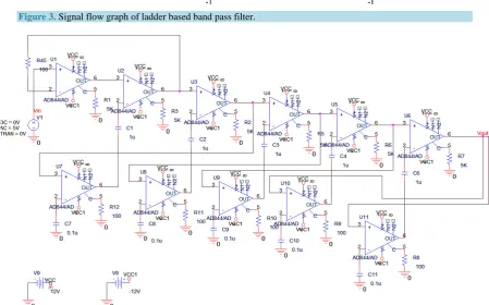
With the help of these equations we make a signal flow graph which has been shown in Figure 3.
2.1.4. CFOA Filter
Using the signal flow graph, CFOA based band pass filter for case 1 has been made as shown in Figure 4.
2.1.5. Observations
[image:4.595.218.478.83.200.2]The passive and CFOA based ladder band pass filter circuits shown in Figure 2 and Figure 4 are designed and
Figure 3.Signal flow graph of ladder based band pass filter.
[image:4.595.88.538.422.702.2]evaluated in PSPICE CAPTURE using conventional resistors, inductors, capacitors and AD844 IC as CFOA. Inductors are used for the passive ladder based circuit.
Now the circuit is simulated in PSPICE CAPTURE and its AC analysis is done.
2.1.6. Response of CFOA Based Band Pass Filter
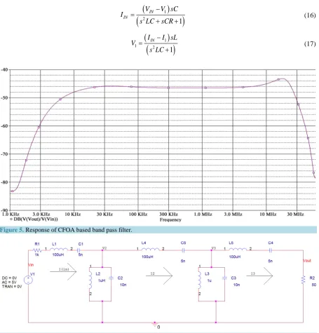
CFOA band pass filter uses the AD844 IC and a power supply to drive it. The circuit is simulated in PSPICE CAPTURE and its AC analysis is done. The graphical output obtained is given below in Figure 5.
2.2. Case 2
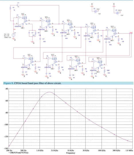
Second model of band pass filter (Figure 6) which was also simulated and the results (Figure 8) are as follows:
2.2.1. Apply KVL and KCL in the Circuit (Figure 6)
(
)
(
2 1)
1
IN IN
V V sC
I
s LC sCR
− =
+ +
(16)
(
)
(
1)
1 2
1
IN
I I sL
V
s LC
− =
[image:5.595.87.543.235.711.2]+ (17)
Figure 5. Response of CFOA based band pass filter.
(
)
(
2)
1 2
1
1
V V s LC
I
sC
− +
= (18)
(
1 2)
2 2
1 I I sL V
s LC
− =
+ (19)
(
)
(
2)
22
1
OUT
V V s LC
I
sC
− +
= (20)
2 2
OUT
V =I R (21)
2.2.2. Conversion into Voltage Form
These equations are converted into voltage form to remove current element and hence we get the following equations:
(
)
(
2 1)
^(
(
2 1)
)
1 1
IN IN
IN IN
V V sCR V V sCR
RI V
s LC sCR s LC sCR
− −
= = =
+ + + + (22)
(
)
(
)
(
(
)
)
^ ^
1 1
1 2 1 2
1 1
IN
IN V V sL
I I sLR
V V
s LC R s LC R
− −
= = =
+ + (23)
(
)
(
2)
(
)
(
2)
1 2 ^ 1 2
1 1
1 1
V V s LC R V V s LC R
RI V
sC sC
− + − +
= = = (24)
(
)
(
)
(
(
)
)
^ ^
1 2
1 2
2 2 2 2
1 1
V V sL
I I sLR
V V
s LC R s LC R
− −
= = =
+ +
(25)
(
)
(
2)
(
)
(
2)
2 ^ 2
2 2
1 1
OUT OUT
V V s LC R V V s LC R
RI V
sC sC
− + − +
= = = (26)
^
2 2 2 2
OUT OUT
I R R V R
V V
R R
= = = (27)
2.2.3. Signal Flow Graph
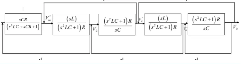
With the help of these equations we make a signal flow graph of the passive ladder based structure of band pass filter (case 2) which has been shown in Figure 7.
The passive and CFOA based ladder band pass filter circuits shown in Figure 6 and Figure 8 are designed and evaluated in PSPICE CAPTURE using conventional resistors, capacitors and AD844 IC as CFOA.
2.2.4. Response of CFOA Based Band Pass Filter (Case 2)
[image:6.595.122.507.605.708.2]For CFOA we use the AD844 IC and a power supply is attached to drive it. The circuit is simulated and its AC analysis is done. The graphical result obtained is shown in Figure 9.
Figure 8. CFOA based band pass filter of above circuit.
Figure 9. Response of CFOA based BPF of model 2.
3. Transformation of Ladder Based Band Stop Filter into CFOA Based Band Stop
Filter
In signal processing, a band-stop filter or band-rejection filter is a filter that passes most frequencies unaltered, but attenuates those in a specific range to very low levels. It is the opposite of a band-pass filter.
filters. Both the input and output terminals are paralleled, and each filter must have a high input and output im-pedance in the band of the other filter to prevent interaction. Therefore, the order n must be odd and the first and last branches should consist of series elements. These restrictions make the design of band-reject filters by com-bining low-pass and high-pass filters undesirable. The impedance interaction between filters is a serious problem unless the separation between cut-offs is many octaves, so the design of band-reject filters is best approached by using a signal flow graph technique to obtain CFOA based bandreject filter from passive ladder based bandreject filter.
Two structures of Ladder Based Band Reject filter has been considered and analysis has been done. These structures have been presented in the two cases as follows:
3.1. Case 1
3.1.1. RLC Based Band Stop Filter
The RLC based band stop filter has been shown in Figure 10.
3.1.2. Mathematical Analysis
After applying KVL and KCL in Figure 10, the following equations have been obtained:
1
in in
A
V V
I R
−
=
(28)
(
)
(
2)
2
1
1
in
I I s LC
V
sC
− +
= (29)
(
)
(
2)
1 2
2
1
V V s LC
I
sL
− +
=
(30)
(
)
(
2)
2 4
2
1
I I s LC
V
sL
− +
=
(31)
(
)
(
2)
2 3
4
1
V V s LC
I
sL
− +
=
(32)
(
)
(
2)
4 6
3 0
1
I I s LC
V V
sL
− +
= = (33)
0 6
B V I
R
[image:8.595.92.540.261.712.2]= (34)
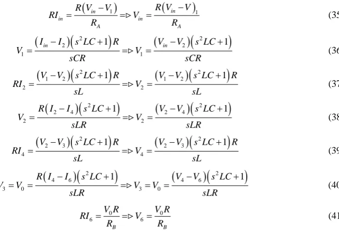
3.1.3. Conversion into Voltage Form
(
in 1)
(
in)
1in in
A A
R V V R V V
RI V
R R
− −
= = = (35)
(
)
(
2)
(
)
(
2)
2 2
1 1
1 1
in in
I I s LC R V V s LC
V V
sCR sCR
− + − +
= = = (36)
(
)
(
2)
(
)
(
2)
1 2 1 2
2 2
1 1
V V s LC R V V s LC R
RI V
sL sL
− + − +
= = = (37)
(
)
(
2)
(
)
(
2)
2 4 2 4
2 2
1 1
R I I s LC V V s LC
V V
sLR sLR
− + − +
= = = (38)
(
)
(
2)
(
)
(
2)
2 3 2 3
4 4
1 1
V V s LC R V V s LC R
RI V
sL sL
− + − +
= = = (39)
(
)
(
2)
(
)
(
2)
4 6 4 6
3 0 3 0
1 1
R I I s LC V V s LC
V V V V
sLR sLR
− + − +
= = = = = (40)
0 0
6 6
B B
V R V R
RI V
R R
= = = (41)
3.1.4. Signal Flow Graph
The Signal Flow Graph of band reject filter has been shown in Figure 11.
3.1.5. CFOA Based Active Ladder Filter
The circuit diagram for CFOA based band stop filter has been shown in Figure 12.
The Signal Flow Graph was analysed and the blocks were converted to CFOA diagram. The passive and CFOA based ladder band reject filter circuits shown in Figure 10 and Figure 12 are designed and evaluated us-ing conventional resistors, inductors, capacitors and AD844 IC as CFOA.
3.1.6. Frequency Response (Gain vs Frequency Response)
The circuit is simulated and its AC analysis is done. The graphical result obtained is shown in Figure 13.
3.2. Case 2
Second model of ladder based Band Reject Filter has been considered and following results were obtained.
3.2.1. Circuit Diagram of Band Reject Filter
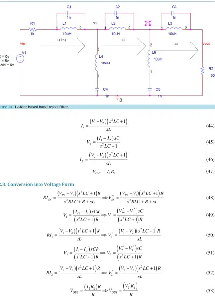
The circuit diagram of ladder based band reject filter has been shown in Figure 14.
3.2.2. Mathematical Analysis
[image:9.595.184.533.100.342.2]After applying KVL and KCL in Figure 14, the following equations have been obtained:
Figure 12. CFOA based band reject filter.
Figure 13.Response of CFOA based BRF.
(
)
(
2)
12
1
IN IN
V V s LC
I
s RLC R sL
− +
=
+ + (42)
(
1)
1 2 1
IN
I I sC V
s LC
− =
Figure 14. Ladder based band reject filter.
(
)
(
2)
1 2
1
1
V V s LC
I
sL
− +
= (44)
(
1 2)
2 2
1
I I sC
V
s LC
− =
+ (45)
(
)
(
2)
2 3
2
1
V V s LC
I
sL
− +
= (46)
2 2
OUT
V =I R (47)
3.2.3. Conversion into Voltage Form
(
)
(
2)
(
)
(
2)
1 ^ 1
2 2
1 1
IN IN
IN IN
V V s LC R V V s LC R
RI V
s RLC R sL s RLC R sL
− + − +
= = =
+ + + + (48)
(
)
(
)
(
(
)
)
^ ^
1 1
1 2 1 2
1 1
IN
IN V V sC
I I sCR
V V
s LC R s LC R
− −
= = =
+ + (49)
(
)
(
2)
(
)
(
2)
1 2 ^ 1 2
1 1
1 1
V V s LC R V V s LC R
RI V
sL sL
− + − +
= = = (50)
(
)
(
)
(
(
)
)
^ ^
2 3
1 2
2 2 2 2
1 1
V V sC
I I sCR
V V
s LC R s LC R
− −
= = =
+ + (51)
(
)
(
2)
(
)
(
2)
2 3 ^ 2 3
2 2
1 1
V V s LC R V V s LC R
RI V
sL sL
− + − +
= = = (52)
(
)
(
^)
2 2 2 2
OUT OUT
V R I R R
V V
R R
= = =
(53)
3.2.4. Signal Flow Graph
3.2.5. Conversion of Ladder Based Band Reject Filter into CFOA
The CFOA obtained after transforming passive ladder based bandreject filter into CFOA based bandreject filter has been shown below in Figure 16.
3.2.6. Frequency Response (Response for Case 2)
For CFOA we use the AD844 IC and a power supply is attached to drive it. The circuit is simulated and its AC analysis done. The graphical result obtained is shown in Figure 17.
4. Simulation Results
Simulation results of both the cases of Band Pass & Band Reject Filter are as follows:
4.1. Band Pass Filter
In Case 1, A Band Pass Filter is simulated with R1=R2 =R3 =R4 =R5 =R6 =R7 =5 kΩ and
8 9 10 11 12 100
R =R =R =R =R = Ω. Taking C1 =C2 =C3 =C4 =C5 =1 uF and
7 8 9 10 11 0.1 uF
C =C =C =C =C = .
In Case 2, A Band Pass Filter is simulated with R1=R2=R3=R4=R5=R6=R7 =10 kΩ and
[image:12.595.86.542.244.710.2]Figure 15. Signal flow graph of band reject filter (case 2).
Figure 17. Response of above BRF.
Table 1. Results of proposed realisation.
Filter Case Active Elements External Resistors External Capacitors
Band Pass Filter Case 1 11 CFOA 11 Grounded 5 Grounded
Case 2 9 CFOA 9 Grounded 5 Grounded
Band Reject Filter Case 1 11 CFOA 11 Grounded 5 Grounded
Case 2 9 CFOA 9 Grounded 5 Grounded
8 9 10 11 12 1
R =R =R =R =R = Ω. Taking C1 =C2 =C3 =C4 =C5 =50 nF and C7 =C8 =C9 =C10=5 nF.
4.2. Band Stop Filter
In Case 1, A Band stop Filter is simulated for R1=R2=50Ω, R3=R4 =R5 =R6 =R7 =50 kΩ and
8 9 10 11 12 50
R =R =R =R =R = Ω. Taking C1=C3 =C5 =C7 =C9 =1 pF, C2=0.1 nF and
4 6 8 10 5 nF
C =C =C =C = .
In Case 2, Band stop Filter is simulated for R1=50Ω, R2=100 kΩ, R3=R4=R5=1 kΩ,
6 7 5 k
R =R = Ω and R8=R9=R10=1 kΩ. Taking C1=C3=C4=C5=10 pF, C2=1 nF and
7 6 8 1 nF
C =C =C = .
5. Conclusions
A systematic method using signal flow graph technique has been developed for converting passive ladder band pass and band reject filter into CFOA based band pass and band reject ladder filter. Such realisations are suitable for fabrication in integrated circuit technology. The CFOA based filters works satisfactorily at higher frequen-cies.
In the proposed configuration, we have used CFOA and resistors and capacitors for realising band pass and band reject filter. Most of the Capacitors which have been used in our configuration are grounded in nature. The grounded devices are easy to fabricate in VLSI chip. The filter configuration designed in the proposed configu-ration has replaced the inductor completely which reduce the size of the circuit and hence, make it less bulky and expensive which is a major requirement of VLSI design.
The summary of the components used, the various frequencies and the bandwidth of band pass and band re-ject filter used in our configuration has been illustrated in Table 1.
fabrica-tion of integrated circuit technique as we replace the inductor with the equivalent CFOA.
References
[1] Lee, S.-S., Zele, R.H., Allstot, D.J. and Liang, G. (1993) CMOS Continuous-Time Current-Mode Filters for High- Frequency Applications. IEEE Journal of Solid-State Circuits, 28, 323-329. http://dx.doi.org/10.1109/4.209999
[2] Ramirez-Angulo, J., Sanchez-Sinencio, E. and Robinson, M. (1992) Current-Mode Continuous Time Filters: Two De-sign Approaches. IEEE Transactions on Circuits and Systems II: Analog and Digital Signal Processing, 39, 337-341.
http://dx.doi.org/10.1109/82.145290
[3] Hughes, B.J., Bird, C.N. and Macbeth, C.I. (1989) Switched Current—A New Technique for Analog Sample-Data Signal Processing. Proceedings of IEEE ISCAS, Portland, May 1989, 1584-1587.
[4] Wu, J. and El-Masry, E. (1996) Current-Mode Ladder Filters Using Multiple Output Current Conveyors. IEE
Pro-ceedings—Circuits, Devices and Systems, 143, 218-222. http://dx.doi.org/10.1049/ip-cds:19960490
[5] Wu, J. and El-Masry, E. (1997) A New Approach of Design of Current-Mode Filters. Proceedings of IEEE
Interna-tional Symposium on Circuits and Systems, 1, 317-320.
[6] Jurisic, D., Mijat, N. and Moschytz, G.S. (2005) Low-Sensitivity Current-Mode Active-RC Filters Using Impedance Tapering. IEEE International Symposium on Circuits and Systems, 4, 3303-3306.
http://dx.doi.org/10.1109/iscas.2005.1465334
[7] Rathore, T.S. and Khot, U.P. (2008) CFA-Based Grounded-Capacitor Operational Simulation of Ladder Filters.
Inter-national Journal of Circuit Theory and Applications, 36, 697-716. http://dx.doi.org/10.1002/cta.456
[8] Sinha, P.K., Saini, A., Kumar, P. and Mishra, S. (2014) CFOA Based Low Pass and High Pass Ladder Filter—A New Configuration. Circuits and Systems, 5, 293-300. http://www.scirp.org/journal/cs