with pulse clocking scheme. The register is design with group of sub shift registers and synchronized with non-overlapping clock pulses generated through a pulse clock generator.The use of latch in shift register creates timing problems which can be avoided by using pulse clock base latches as a basic cell in shift register. This resolve the timing problem created in shift register by using several non-overlapping clock in a duration of pulses. The shift register cell CMOS layout is design using 50nm technology in MICROWIND layout simulator tool. Total 2890 transistors are require for this design. The simulation analysis shows that the area of latch using 50nm technology is 2.8125 μm2. The power dissipation for 256 bit
length shift register is computed as 41.3μW with the area of 3162 μm2.
Keywords – Pulse Clock, Latch.
I.
I
NTRODUCTIONThe shift registers are mainly use in memory designs of microprocessors and microcontroller.It is one of the fundamental block used in digitalintegrated circuits. Shift registers are mainly used in microcontrollers, microprocessors, communication system devices such as receiver circuits, filters, memory design, image processing IC’s etc. In shift register a string of N numbers of flip flop base register is synchronized with a common clock. The number of flip flops are series connected through a synchronized clock input to design shift. The speed of the flip-flop is not as much essential than the area and power consumption because there is no combinational logic
timing problems related to the pulse latch as when pulsed latches are used instead of flip flops in several applications because of less numbers of transistors is required in pulse latch as compared to that of a flip flop.Generally latches are not use in shift register design because of timing problems though it reduces the number of transistors and are of design.
This paper discusses the design of 256 latch base shift register with area and power optimization synchronized with pulse clocking scheme.
II. C
ONVENTIONALS
HIFTERThe structure of shift register consist of series connected flip flop with a synchronized clock input. All flip‐flops receive common clock pulses, which activate the shift of data from one stage to the next. Synchronization is achieved by a timing device called clock generator, which provides a clock signal having the form of a periodic train of clock pulses. The clock signal is commonly denoted by the identifiers clock and clk. The clock pulses are distributed throughout the system in such a way that storage elements are affected only with the arrival of each pulse. In practice, the clock pulses determine when computational activity will occur within the circuit, and other signals determine what changes will take place affecting the storage elements and the outputs.
Fig. 2. Timing Simulation of Conventional Shift Register
III. R
ELATEDW
ORKThe area and power consumption of shift register are optimizes by using clock pulse latch instate of flip-flops in design [1]. The shift register is design by series connected clock pulse latches in a group. The several such groups of sub shift registers along with clock pulse generator. This circuit avoids the timing problems of conventional shift register. In [1] a 256-bit shift register using pulsed latches was fabricated using a 0.18 CMOS process with. The core area is. The power consumption is 1.2 mW at a 100 MHz clock frequency. The proposed shift register saves 37% area and 44% power compared to the conventional shift register with flip-flops [1].
In [2] a Low power clock-gated synchronous counter using Logical Effort (LE) optimized Transmission-gate Master- Slave Flip-Flop (TGMS FF) is proposed. Logical Effort is the transistor width optimization methodology for providing a tradeoff between area, delay and power.Logical Effort theory is the manual method for optimizing the transistor width. Out of all logic circuits, Inverter is said to
be a best driver. Even a simple NAND gate will be slower than a inverter because of its topology. Hence Logical Effort uses inverter as a reference circuit and compares the driving capabilities of given gate with it [2].
In [3] a adaptive coupled flip flop circuit is use for power dissipation optimization.
In [4] Flip flop and latch designs include many timing element that are not on the critical path and this timing slack can be exploited by sing slower, lower energy TEs. Instead of simultaneously optimizing for delay and energy, critical TEs should be optimized to reduce delay and noncritical TEs should be optimized to reduce energy. Design results shows energy reduction of 63% with no loss in performance compared to a high-performance design with homogeneous flip-flop and latch structures. Compared to a design which uses transistor sizing alone to reduce energy, activity-sensitive selection results in a further total TE energy reduction of 46% [4].
Fig. 4. Timing Simulation of Pulse Shifter
IV. T
WOH
UNDRED ANDF
IFTYS
IX BITP
ULSELATCH SHIFT
R
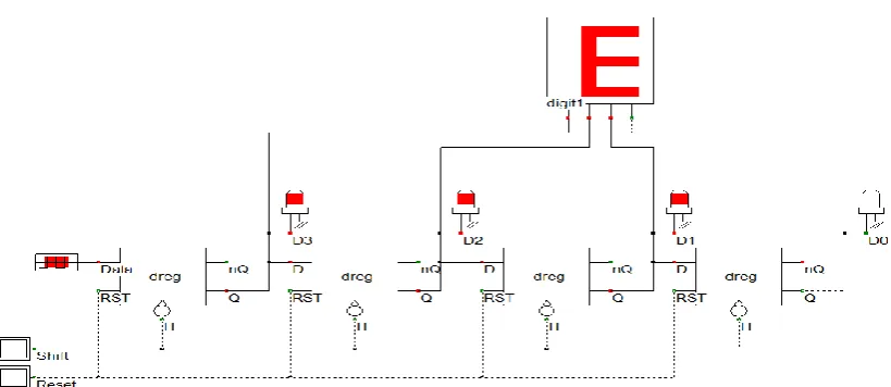
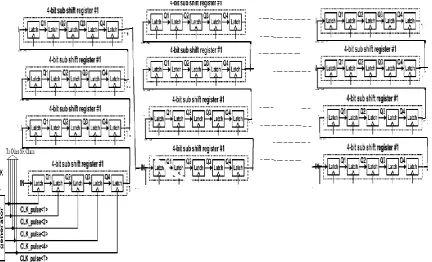
EGISTERThe fig shows the 256 bit pulse latch shift register circuit. The proposed shift register is divided into 64 sub shifter registers to reduce the number of delayed pulsed clock signals. The architecture of 256 bit register is similar to that of 8, 16 and 32 bit registers. A 256 array chain of 4 latch is connected to the four non-overlap delayed pulsed clock signals (clk0, clk1, clk2, clk3). In the 4-bit sub shift
register1, four latches store 4-bit data (Q1-Q4) and similarly the clock pulses are connected to the next chain of 4 bit shift register.
This register requires 256 latches comprises of 512 transmission gates and 768 NOT logic gates. The total number of transistors for this design is 2890 for shift register chain. The operations of the other sub shift registers are the same as that of the sub shift register1 except that the first latch receives data from the temporary storage latch in the previous sub shift register
.
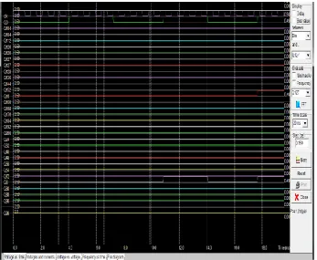
Fig. 6. Timing Simulation for 256 bit pulse clock shift register
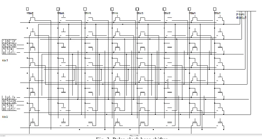
The 256 bit shift register is divided into sub shifter registers to reduce the number of delayed pulsed clock signals. A 4-bit sub shifter register array is synchronized through the parallel connected clock pulses through clock generator. That is clcok0 is connected to the first latch of each array. Similarly the clock1, clock2 and clock3 are connected to second, third and fourth latch of each sub shift register array. When 256 bit shift register is divided into 4 bit sub shift registers, the number of clock-pulse circuits is of 4 bit and the number of latches is 256. A sub shift register consisting of 4 latches requires pulsed clock signals. Each sub shift register has a temporary storage latch. The designed shift register is decompose into series connected sub registers to reduce the number of delayed pulsed clock signals. A 4-bit sub shifter register consists of five latches and it performs shift operations with five non-overlap delayed pulsed clock signals. In the 4-bit sub shift register 1, four latches store 4-bit data (Q1-Q4) and the last latch stores 1-bit temporary data (T1) which will be stored in the first latch (Q5) of the 4-bit sub shift register 2. Fig.... shows the operation waveforms in the proposed shift register.Total 2890 transistors are require for this design. The outputs of clock generator are connected to the clock inputs of each latch.
Table I: Comparative Analysis
Type [1] This Work
Transistor Size
(μm/μm) NMOS 0.5/1.8 PMOS 0.5/1.8 PMOS 0.05/0.15 NMOS 0.05/0.1 Latch area (6.7μmX5.6μm) 19.2 μm2 (2.25μmX1.25μm) 2.8125μm2 Latch Power
Dissipation 3.30 μW 0.209μW
Number of Transistors in
Latch 7 10
Word Length 256 256
Total number of Pulse Latch in Shift Register (PLSR)
320 256
Power Dissipation (PLSR)
1.99mW 41.3μW
Area (PLSR) 6600 3162 μm
2 (115 μm X 27.5
problem of pulse latch base shift register is resolve by using the non overlap clock pulses. These pulses are generated from clock pulse generator.
R
EFERENCES[1] Byung-Do Yang "Low-Power and Area-Efficient Shift Register Using Pulsed Latches" IEEE Transactions On Circuits And Systems—I: Regular Papers, Vol. 62, No. 6, June 2015 pp no 1564.
[2] Masaki Masuda, Kanto Kubota, Ryosuke Yamamoto, Jun Furuta, Kazutoshi Kobayashi, and Hidetoshi Onodera "A 65 nm Low-Power Adaptive-Coupling Redundant Flip-Flop" IEEE Transactions On Nuclear Science, Vol. 60, No. 4, August 2013 pp no 2750.
[3] K. Kobayashi, K. Kubota, M. Masuda, Y. Manzawa, J. Furuta, S. Kanda, and H. Onodera "A Low-Power and Area-Efficient Radiation-Hard Redundant Flip-Flop, DICE ACFF, in a 65 nm Thin-BOX FD-SOI" IEEE Transactions On Nuclear Science, Vol. 61, No. 4, August 2014 pp no. 1881.
[4] A.ParvathiKarthica "Power Efficient Synchronous Counter Using Transmission-Gate Based Master-Slave Flip-Flop With Modified Logical Effort Optimization" International Conference on Electronics and Communication Engineering (ECE) 7th April 2013 ppno. 86.
[5] S. EhsanRazavi, "Shift Register Design Using D-Flip flop with Low Power Consumption and High Speed " International Journal of Science and Advanced Technology (ISSN 2221-8386) Volume 1 No 7 September 2011.
[6] Ch. DayaSagar, T. Krishna Moorthy "Design of a Low Power Flip-Flop Using MTCMOS Technique" International Journal of Computer Applications & Information Technology Vol. 1, No.1, July 2012.
A
UTHOR’
SP
ROFILEMd. Ajaz Ahmad