Self-powered transparent glass-based single electrode triboelectric motion
tracking sensor array
Jinkai Chen1, Peng Ding1, Ruizheng Pan1, Weipeng Xuan1, Dapeng Guo2, Zhi Ye1, Wuliang Yin3, Hao Jin1, Xiaozhi Wang1, Shurong Dong1* and Jikui Luo4, 5*
1. Coll. of Info. Sci. & Electron. Eng., Zhejiang University, 38 Zheda Road, Hangzhou 310027, China. 2. Dept. of Appl. Phys., Chang’an University, Xi’an 710064, China.
3. Sch. of Elec. and Electron. Eng., The University of Manchester, Manchester M60 1QD, U.K. 4. Coll. of Electron. & Info. Hangzhou Dianzi University
5. Inst. of Renew. Energy & Environ. Technol., Bolton University, Deane Road, Bolton BL3 5AB, UK
Abstract: A glass-based single electrode triboelectric generator (SETEG) is developed with polydimethylsiloxane (PDMS) as the negative material. Its performance under different contact forces, frequencies and spacers is investigated in detail. The SETEGs have higher electric output under higher contact force, frequency and spacer, and show better performance with a thinner glass layer at lower humidity condition. An open circuit voltage, short circuit current and power up to 318 V, 8.3 μA and 427 μW are obtained for a SETEG of 5×5 cm2 size. Based on the study, a tracking sensor array consisting of nine 5×5 mm2 SETEGs is proposed and developed. A LabVIEW-based automatic measurement system is also developed to record, process and display the real-time output voltages of the sensing array. Results show that an output voltage up to 4 V can be easily generated when a PDMS-covered stylus touches/slides the sensor array, and the output voltages from different sensors are independent from each other. This work demonstrates the great application potential of the SETEGs sensor array for self-powered detection, tracking or monitoring motion or a touch of a stylus or some objects, thus would be very useful for touch screen display, handheld tracking device, domestic security, traffic monitoring etc.
Keywords: triboelectric generator, transparent, glass based TEG, self-powered sensor array
1. Introduction
With the rapid development of the Internet of Things, the complementary energy sources
choices for complementary energy sources, which are based on piezoelectric[1, 2],
pyroelectric[3, 4] and triboelectric[5, 6] effects etc. The triboelectric generator (TEG) uses
the contact of two materials with opposite electronic affinities to convert waste mechanical
energy into electric energy, and it is considered to be one of the most promising energy
harvesting devices due to its simple device structure, low cost, easiness for large-scale
fabrication, and most importantly, the high electrical output compared with other energy
harvesting technologies. TEGs can generate electric energy through three types of operation
modes, which are the vertical contact, lateral slide and single electrode mode. As only one of
the charge materials is connected to the circuit, the single electrode TEG (SETEG) is not the
best form for energy harvesting due to its small quantity of generated electricity[7] compared
with other two modes. However, this structure is more suitable for daily life applications as it
not only can be used to harvest energy, but also can be self-powered sensors for many
applications, as other unconnected material can be anything such as rain drop[8], finger[9, 10]
and pavement[11] etc. A SETEG array on polymer substrates has been utilized to fabricate
tactile sensor or pressure sensors[12, 13], mostly by utilizing finger touch for displaying
information, demonstrated their usefulness and allocation potential. Polymer substrates are
excellent materials for flexible applications, but they are still not widely used in electronic
devices and systems yet.
Glass has the advantages of high transparency, excellent corrosion and wear resistance,
thermal reliability and hardness etc, which is also relatively more suitable for the mass fabrication compared with polymer based TEG sensor. It has been widely used in our daily
life from skyscrapers to mobile phones in our hands. The glass-based contact mode TEGs
have shown good electrical output and excellent mechanical reliability and stability by our
previous work[14], though no practical glass-based TEG application has been reported yet.
So compared with TEG made with flexible polymer triboelectric materials, the glass based SETEG can also be very important in some specific areas that require a triboelectric materials with high thermal and mechanical reliability.
Here we report further development of the transparent SETEG-based tracking sensor
array using commercially available glass and a polydimethylsiloxane (PDMS) covered touch
and power up to 318 V, 8.3 μA and 427 μW, respectively, while the SETEG sensor (5×5 mm2
pixel size) array has a voltage output larger than 4 V under ~1 N contact force, which can be
easily detected by a commercial analog to digital converter (ADC). Results demonstrate that
the glass-based SETEG and its sensor array have great potential to be integrated into widely
available glasses for much broader applications, such as touch screen displays, hand-held motion tracking devices, domestic security or display, and can be fabricated with much
higher resolution. We also highlight the “ghosting effect” of the tracking sensor, that links the
output of one pixel with others, and the methods to suppress the effect.
2. Fabrication and experimental setup
Before fabricating the tracking sensing array, we firstly investigated the performance of
the SETEG systematically using glass and PDMS as the charging materials. The completed
5×5 cm2 SETEG structure with the upper PDMS part and the lower glass part is shown in Fig.
1(a). The PDMS (184 Silicone Elastomer, Dow corning Co. Ltd.) solution, which was a
mixture of the base PDMS and the crosslinker at a ratio of 10:1 by mass, was spun on a
commercially available 1 mm soda lime glass at 1100 rpm for 10 sec to obtain a PDMS thin
film with a thickness of ~100 μm (note this glass was merely used as a mechanical supporter,
and can be replaced by any other rigid material). Then the PDMS layer on the glass substrate was cross-linked on a hot plate at 100 °C for 25 min. The lower glass part consists of a
commercially available soda lime glass with different thicknesses (0.55, 1, 2 and 3 mm), a
transparent indium tin oxide (ITO) conductive thin layer (thickness is 750 nm with a
resistivity of 3.525×10⁻⁴Ω∙cm) and an acrylic protective layer. The ITO layer was deposited
on the soda lime glass by the direct-current reactive magnetron sputtering at 150 W power,
0.7 Pa pressure and -75 V bias voltage[15]. For a better transparency and conductivity, the
ITO was then annealed using a rapid thermal annealing machine (RTP-CT100M) at 300 °C
for 5 min in N2 atmospheric pressure. Finally, the protective acrylic layer was glued to the
ITO layer. These samples were made for the preliminary test to demonstrate its capability to
be used as TEG sensor array.
contact force, frequency and spacer between the two TEG electrodes, which is the same as
the experimental setup in our previous work[14]. The voltage and current outputs were
collected using an oscilloscope (Tektronix MDO3022) and a picometer (Keysight B2981A),
respectively.
Fig. 1(b) is the three dimensional (3D) illustration of the sensing array device (0.55 mm
thickness, 5×5 cm2) with nine SETEGs (the pixel size is 5×5 mm2 with a 5 mm distance
between pixels in both the x- and y-directions). The ITO pattern on the glass wafer was
fabricated using the conventional ultraviolet light photolithography and lift-off process and it
was then deposited and annealed using the same conditions mentioned above. The central
nine squares of the ITO patterns were the electrodes for the nine SETEGs, and the relatively
smaller nine squares around were designed for the connection of the sensor array wafer and
the PCB using the conductive tape, which is shown in Fig. 1(c). The PCB was designed to
have a hollowed square window to demonstrate the good optical transparency of the sensor
array wafer, and the image on the computer screen can be seen clearly with the sensor array
wafer on it.
Fig. 1. 3D illustration of the SETEG with the glass and PDMS parts (a) and the tracking sensing array wafer (b).
The sensing array was connected to a central hollowed printed circuit board (PCB) using conductive tape,
showing good optical transparency (c), and a stylus with a PDMS covered head was touching or sliding on the
glass side of the sensing array wafer during the test (d). The voltage data from nine independent SETEGs on the
sensing array wafer were collected using a DAQ card (e). Note the glass used is the upper part of TEG (a) is
Fig. 1(d) shows the test configuration of the sensor array, a stylus with a PDMS layer
covered head was touching or sliding on the front side (glass side) of the sensing array device
with the back side (ITO side) of the sensing array device shown in Fig. 1(b). The contact area
of the stylus soft head is much smaller than 25 mm2 (the maximum area of the stylus), depending on the contact force applied, and the PDMS layer thickness is approximately 100
µm formed by dip coating. The voltage signals were collected using a data acquisition (DAQ)
USB card (Adlink USB 1902) connected to a computer, as shown in Fig. 1(e). A
self-developed LabVIEW program was then used to calculate the voltage data from the nine
independent SETEGs to display the real-time voltage curve and tracking animation on the
computer screen.
3. Results and discussion
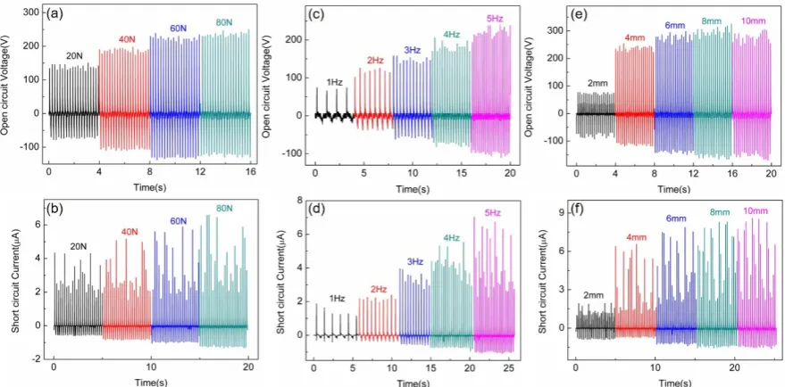
The SETEGs with 0.55 mm glass were cyclically tested under different contact forces,
frequencies, spacers. Figs. 2(a) and (b) show the open circuit voltage and short circuit current
of the TEG with a 4 mm spacer at a 5 Hz contact frequency under different contact forces,
respectively. The open circuit voltage steadily increases from 146 V (20 N) to 238 V (60 N),
and then gradually goes up to 250 V when the contact force reaches 80 N. The short circuit
current experiences a similar trend, which increases from 4.3 μA to 6.6 μA when the contact
force increases from 20 N to 80 N.
There are two main reasons that enhance the electric output of the contact mode glass
based TEG under higher contact forces according to our previous work[14], which are the
increase of the contact area and the total capacitance of the TEG[16]. The capacitance
increase of the PDMS part in the TEG is the primary reason that results in the total
capacitance increase of the TEG, because glass is a rigid material and higher contact force
will only compress the PDMS layer, leading to a smaller thickness, which means a larger flat
panel capacity of the PDMS part. For the SETEG, the PDMS part has not electrically linked
to the TEG, so the total capacity of the TEG actually remains almost unchanged. Only the
increased contact area enhances the electric output performance under higher contact force,
and that’s the reason why the electric output improvement of the glass based SETEG under
The open circuit voltage and short circuit current with a 50 N contact force and a 4 mm
spacer under different contact frequencies are shown in Figs. 2(c) and (d). The open circuit
voltage gradually increases from 74 V to 238 V when the frequency increases from 1 Hz to 5
Hz, and the short circuit current shows the similar trend, gradually increasing from 1.9 μA (1
Hz) to 7 μA (5 Hz). The rising trend of the electric output can be attributed to the quicker
contact speed under higher frequency, which leads to a faster induction and movement of
charges as discussed in our previous work [14]. Figs. 2(e) and (f) illustrate the open circuit
voltage and short circuit current with 50 N contact force and 5 Hz contact frequency under
different spacers, respectively. It is clear from these two figures that the electric output
saturate when the spacer is larger than 8 mm. The open circuit voltage and short circuit
current are 75 V and 1.9 μA at 2 mm spacer, followed by a sharp increase to 254 V and 6.6 μA when the spacer is 4 mm, then a slight increase to 318 V and 8.3 μA at 8 mm spacer. As
the contact frequency is the same for different spacer conditions, higher spacer means higher
relative velocity of the PDMS and glass triboelectric layers, which leads to a faster charge
transferring speed, thus a better electric output performance.
Fig. 2. The open circuit voltage (a) and short circuit current (b) of the glass based SETEG increase slightly with
increase in contact force. The open circuit voltage (c) and short circuit (d) of TEG increase when contact
frequency rises from 1 Hz to 5 Hz. The open circuit voltage (e) and short circuit current (f) experience a sharp
Besides the tests of the SETEG performance under different contact conditions, we have
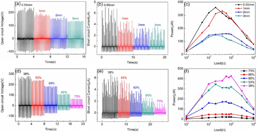
also measured the electric output performance of the glass based SETEGs with different
environmental humidity and thicknesses of glass. Figs. 3(a), (b) and (c) show the open circuit
voltage, short circuit current and power of the SETEG with four different glass thicknesses
under a 50 N contact force, a 5 Hz contact frequency and a 4 mm spacer, respectively. The
open circuit voltage gradually decreases from 238 to 135 V when the glass thickness
increases from 0.55 to 3 mm. The short circuit shows a similar trend, which decreases from
7.1 to 3.5 μA as the glass thickness increases from 0.55 to 3 mm. It can be seen clearly from
Fig. 3(c) that the peak power is possibly between a glass thickness of 0.55 mm and 1 mm,
which is 359.1 and 331.7 μW for 0.55 and 1 mm glass thickness, respectively. With further increase of the glass thickness, the peak power declines dramatically to 159.3 μW when the
glass thickness reaches 2 mm, and then the decrease trend becomes smooth again. The peak
power of the TEG with 3 mm glass drops slightly to 149.1 μW. The downtrend of the peak
power might be attributed to the larger portion of charges lost during the propagation from
the surface of a thicker glass to the ITO electrode.
Fig. 3. Open circuit voltage(a), short circuit current (b) and power (c) of SETEG with different glass thicknesses
(0.55 mm, 1 mm, 2 mm and 3 mm), decreasing with the increasing glass thickness. open circuit voltage(d), short
circuit current (e) and power (f) under different humidity levels, decreasing with the increasing humidity.
reported, higher humidity level will lead to the electric output deterioration due to the
inducted charge leakage on the surface of the triboelectric material[17], the measurement of
the open circuit voltage, short circuit current and power under different humidity, is
extremely important. We have conducted the measurements with the results shown in Figs.
3(d), (e) and (f). The open circuit voltage decreases from 282 V at 38%RH (relative humidity)
to 61 V of 73%RH, and the short circuit current declines from 6.6 μA to 1.6 μA when the
humidity increases from 38%RH to 73%RH. For the peak power, it is only 21.4 μW at 73%RH, and dramatically increases to 427 μW at RH 38%RH. The power output at high
humidity level is undoubtedly too small for the energy harvesting application, but it is
sufficient for the sensing applications as the commercial ADC can easily measure voltage
signal in millivolt scale.
The stability is one of the most important criteria to decide if the sensors are good or not.
Fig. 4 is the open circuit voltage of a SETEG with a 0.55 mm glass cyclically tested for more
than 10000 periods. The initially tested open circuit voltage is 322 V, and it slightly rises to
350 V after 3000 periods’ contact. After that, the open circuit voltage remains stable until the
end of the test. The increase of the open circuit voltage can be explained by the better contact
of the PDMS layer with the glass after initial tests, which leads to a larger contact area.
Fig. 4. The open circuit voltage of the SETEG with a 0.55 mm glass cyclical tested for more than 10000 periods,
demonstrating its excellent stability.
The above experiments have clearly demonstrated the feasibility of using the commercial
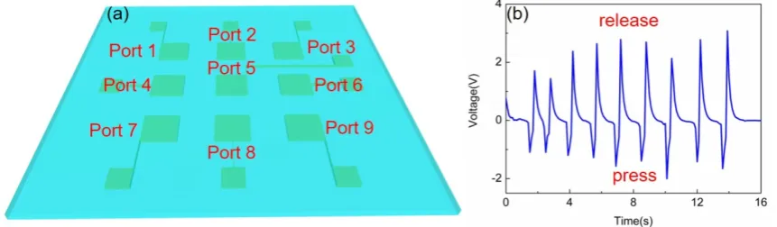
front side (glass side) of the sensor array wafer. There are nine independent SETEG sensors
made on a glass wafer, and they have been numbered from Port1 to Port9. An automatic
measurement system was built to record, process and display the voltage outputs of the
sensing array under the contact of the PDMS-covered stylus. Fig. 5(b) shows the voltage
output of Port1 recorded by the DAQ when touched by the stylus. A negative voltage and
positive voltage are generated when the stylus presses on and releases from the glass surface,
respectively. For the sliding movement of the stylus, a negative voltage is generated when the
stylus first approaches the sensor electrode and a positive voltage is generated when the
stylus leaves the sensor electrode. The generated voltage is not as large as the results tested
under the dynamic fatigue tester as the contact area of the stylus and contact force are very
small (~1 N, < 25 mm2), but the voltage outputs are large enough for any commercial DAQ to
process. ITO electrodes were only used as the conductive electrode to collect charges (signal)
for the SETEG sensors, with the pixel size of 5×5 mm2 for this work. For a 1 mm2 pixel, the
output voltage is over 100 mV, and can be easily measured by ADC, though noise would be
an issue. Therefore we speculate the tracking sensor could have pixel size down to
submillimeter for high resolution application.
Fig. 5. 3D illustration of the front side (glass side) of the sensing array wafer and the nine separated SETEG
sensors have been numbered from Port1 to Port9 (a), and DAQ device collected voltage output of Port1 (b). The
negative and positive voltages are generated when the stylus presses on and release from the glass surface,
respectively.
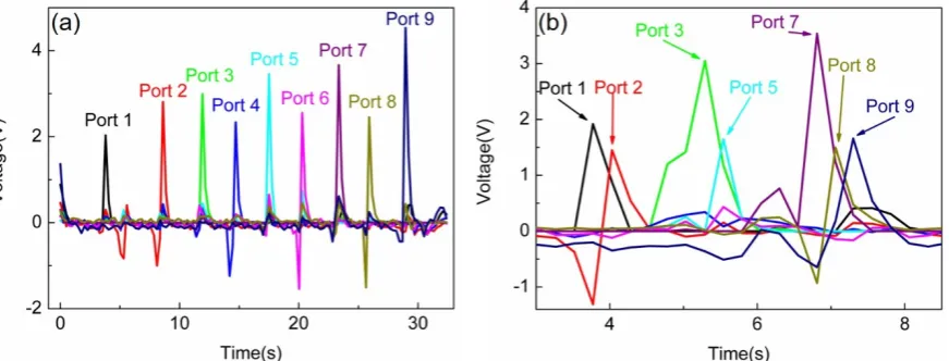
The stack illustrations of voltages of nine ports contacted one by one is shown in Fig.
6(a). Fig. 6(b) shows the voltage output when the stylus slides on the sensing array with a
that when one port is being touched, small voltage signals can also be detected from other
ports. For example, when Port9 is touched at 30 sec (Fig. 6(a)), there is a small voltage
detected from Port1 as well. We have tried to make sensors with different pixel sizes and
different distances between pixels, this phenomenon exists regardless the device size and
structure. This phenomenon is known as the “ghosting effect” and is a common phenomenon
associated with the operation method of a DAQ and ADC as discussed later. Therefore it is
necessary to pay attention to this when designing a tactile sensor with SETEG array,
especially for high speed applications.
Fig. 6. Stacked voltage pictures for 9 ports touch independently (a) and being slided with Z type (b) by a PDMS
covered stylus, showing a good independence of the nine SETEG sensors.
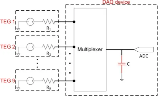
The ghosting effect can be explained using the operation principle of a DAQ device. As
shown in Fig. 7, a commercial economic DAQ usually only has one ADC, and a multiplexer
is used to switch from one channel to another when performing a multi-channel measurement.
This means that only one channel can be recorded at a time even for a multi-channel setup.
When the multi-channel analog signals come into the DAQ device, the multiplexer will
choose one of the signals and let it charge the capacitor C in the front of the ADC to reach the
voltage to the source signal voltage is called the setting time. After the conversion of the first
channel data into digital one completed, the multiplexer will switch to the next channel, and
the capacitor C starts to charge or discharge from the voltage of the previous channel to the
voltage of the channel connected. For common analog source, the DAQ device works
perfectly, but TEG has a very large input impedance (R1 to R9 as shown in Fig. 7), ranging
from tens to hundreds of MΩ, which means it will take much longer time for a TEG device to
charge or discharge the capacitor C (higher setting time). For instance, after the conversion of
Port9 voltage, the capacitor C has a high voltage and when the multiplexer switches to Port1,
as the source analog signal of Port1 is 0 V, the capacitor C will discharge to 0 voltage, but the
high input impedance requires a much longer setting time, which means it can not be
discharged to 0 V before the next channel is switched on and the ADC records a voltage
higher than 0 V for Port1.
Fig. 7. A schematic diagram of the multi-channel DAQ device collecting data from nine independent TEG
sensors. The over-large input impedance of SETEG will lead to a ghosting effect.
This effect can be suppressed by using a DAQ device with multiple ADCs or set the
sampling rate low enough or sampling time longer enough for the capacitor C to be charged
or discharged completely. With multiple ADCs, each can operate independently without
affecting others, thus no ghost effect exists. In this work, a single ADC DAQ card was used,
so we set the sampling rate longer at ~ 250 ms per point or 4 Hz to suppress the ghosting
effect, which can be nearly neglected as illustrated in Figs. 6(a) and (b), showing almost
operation frequency can not be very high, limiting their high speed application. This can be
solved by using a DAQ with multiple ADCs and capacitors with small capacitances. The
ghost effect was not reported by others, we speculate the touching by finger and releasing
will take much longer times than the charging/discharging times required, so that no ghost
effect could be observed.
One thing needs to be pointed is that there is no negative voltage output in some of the
ports, for example Port1. This is because the measured voltage output start points of these
ports were set -10 V rather than 0 V as shown in the figure and the low voltage measurement
limit of this DAQ device is -10 V, so that we can not see the negative voltage output in the
figure. For motion tracking, what we want to sense is the output signal when the stylus leaves
the sensor port, which is a positive voltage, and the negative voltage signal is not practically
useful for the application.
Fig. 8. Voltage output under nine independent touch (a) and a Z type sliding (b), showing the capability of the
sensing array to track a motion on the glass surface.
The voltage amplitude of each port under contact can be seen more clearly from Figs. 8(a)
and (b), which are the voltage output under nine independent touches and a Z type sliding,
respectively. The peak voltage in Fig. 8(a) is 2.03, 2.81, 2.99, 2.33, 3.46, 2.55, 3.66, 2.45 and
4.53 V for Port1 to Port9, respectively. The voltage output values are not the same for all the
ports as the force imposed by stylus by hand varies every time. Nevertheless, all the voltage
amplitudes of nine ports are large enough for any commercial DAQ device to collect and
velocity of the stylus can be calculated by dividing the distance over the time between peaks.
The Z type sliding consists of three strokes: Port1-Port2-Port3, Port3-Port5-Port7, and
Port7-Port8-Port9, and the average sliding speed are 1.32, 1.32 and 4.08 cm/s for these three
strokes, respectively. At the turning points of Z type motion in the Port2-Port3 and
Port5-Port7 regions, the hand controlled stylus slides relatively slower to change the direction
of moving, so that it takes more time for the voltage signals to be generated in these parts.
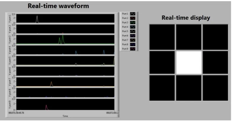
Besides the data recording and automatic measurement system, a real-time motion
tracking display was also developed to show the trace of the stylus movement using
LabVIEW program, which is shown in Fig. 9. The left nine stacked pictures are for the
real-time voltage output display and the right part is used to display the real-time stylus
movement, which have nine squares corresponding to nine ports on the sensing array. As
shown in Fig. 9, when the stylus touches Port5, the corresponding black square turns to white,
and a higher voltage output will result in a whiter square. Two videos (see supplement video
touch.mp4 and slide.mp4) are recorded to demonstrate the feasibility of tracking stylus
movement using the sensing array. This real-time motion tracking system is a prototype
device, for a further triboelectric touch screen (like the existing resistive and capacitive touch
screen) system with a customized DAQ for further suppressing the ghosting effect and a
better multi-channel voltage output measure performance, which is under developing.
Fig. 9. LabVIEW Graphic interface is used to display the real-time voltage output (left) and the trace (right) of
the moving stylus and Port5 is touched for this frame.
particularly useful for touch screen application, the working principle can be applied to other substrate materials, thus this research has demonstrated the great application potential of the
SETEGs sensor array for self-powered detection, tracking or monitoring the motion or a
touch of an object, and it would be particularly useful for the development of touch screen
display, handheld tracking devices, domestic security, traffic monitoring etc.
4. Conclusion
Transparent glass based SETEGs have been made and have been firstly characterized
under different contact forces, frequencies and spacers. Higher contact force, frequency and
spacer lead to higher SETEG electric outputs. SETEGs with different glass thicknesses have
been tested under different humidity. They have a larger electric output with a thinner glass
and at lower humidity. An open-circuit voltage, short-circuit current and power up to 318 V,
8.3 μA and 427 μW have been achieved for a SETEG with an area of 5×5 cm2. The SETEG
cyclically tested for more than 10000 cycles showed no performance deterioration and good
stability. A glass-based SETEG sensor array of nine sensors has been developed to track the
motion of a stylus with a PDMS covered head. Furthermore, A LabVIEW program has been
developed to process and display the real-time voltage output and stylus motion. The 9
separated sensors show good independence from each other for the single port touch test as
well as the capability to track stylus motion. All the above experiments demonstrated the
great potential of the glass-based SETEG to be utilized in our daily life for self-powered
sensing, tracking and display applications.
Acknowledgement: Project was supported by NSFC (Nos. 61274037, 61301046 and 61376118) and “the Fundamental Research Funds for the Central Universities 2016XZZX001-05”. The authors also acknowledge the Innovation Platform of Micro/Nanodevices and Integration System, Zhejiang University. Jinkai Chen acknowledges the Graduate Education International Exchange Fund from Zhejiang University for sponsoring his study at the University of Manchester.
References
[2] P.K. Panda, J. Mater. Sci., 44 (2009) 5049-5062.
[3] S.R. Hunter, N.V. Lavrik, S. Mostafa, S. Rajic, P.G. Datskos, Proc. SPIE, 8377 (2012). [4] I. Lubomirsky, O. Stafsudd, Rev. Sci. Instr., 83 (2012).
[5] F.R. Fan, Z.Q. Tian, Z.L. Wang, Nano Energ., 1 (2012) 328-334.
[6] G. Zhu, C.F. Pan, W.X. Guo, C.Y. Chen, Y.S. Zhou, R.M. Yu, Z.L. Wang, Nano Lett., 12 (2012) 4960-4965.
[7] Y.L. Zi, S.M. Niu, J. Wang, Z. Wen, W. Tang, Z.L. Wang, Nat. Commun., 6 (2015). [8] Q.J. Liang, X.Q. Yan, X.Q. Liao, Y. Zhang, Nano Energ., 25 (2016) 18-25.
[9] Y. Yang, H.L. Zhang, Z.H. Lin, Y.S. Zhou, Q.S. Jing, Y.J. Su, J. Yang, J. Chen, C.G. Hu, Z.L. Wang, Acs Nano, 7 (2013) 9213-9222.
[10] Y. Yang, Y.S. Zhou, H.L. Zhang, Y. Liu, S.M. Lee, Z.L. Wang, Adv. Mater., 25 (2013) 6594-6601. [11] Y.C. Mao, D.L. Geng, E.J. Liang, X.D. Wang, Nano Energ., 15 (2015) 227-234.
[12] X. Wang, H. Zhang, L. Dong, X. Han, W. Du, J. Zhai, C. Pan, Z.L. Wang, Adv. Mater., 28 (2016) 2896-2903.
[13] Z.W. Yang, Y. Pang, L. Zhang, C. Lu, J. Chen, T. Zhou, C. Zhang, Z.L. Wang, Acs Nano, 10 (2016) 10912-10920.
[14] J. Chen, H. Guo, P. Ding, R. Pan, W. Wang, W. Xuan, X. Wang, H. Jin, S. Dong, J. Luo, Nano Energ., 30 (2016) 235-241.
[15] J. Chen, X. He, W. Wang, W. Xuan, J. Zhou, X. Wang, S.R. Dong, S. Garner, P. Cimo, J.K. Luo, J. Mater. Chem. C, 2 (2014) 9109-9114.