MURDOCH UNIVERSITY
ENG460 Engineering Thesis
Charge Transfer Capacitance Meter Development
For Capacitive Level Sensor
Robert Alexander Anderson 18th November 2013
i | P a g e
Acknowledgements
I would like to take this opportunity to express my gratitude to my supervisor, Dr. Gareth Lee for providing me with the guidance required to undertake this thesis project. In addition, a special thank you to John Boulton for his advice and help in constructing my capacitor probes. Finally my heartfelt appreciation goes to my family for their unending support and understanding.
ii | P a g e
Abstract
An innovative technique has been recently developed to measure capacitance and capacitive touch. This technique labeled ‘QTouch’ was patented to Atmel in 2011, [1] but invented by a firm called ‘Quantum Research Group’. The heart of this thesis focuses on two different types of capacitive sensing circuits, adapted from the ‘QTouch’ technique.
The first circuit involves a ‘charge divider’ approach, which behaves similar to resistive voltage divider circuitry, where a voltage is retrieved between a pair of capacitors to compute the unknown
capacitance. The key advantage of this circuitry is that it allows a microcontroller to narrow the analogue reference (AREF), which focuses a maximum analogue input range on a linear region. It also has the advantage of obtaining a differential capacitance measurement through using a fixed/known reference capacitor. And finally, it offers a measurement for each charge cycle. In the second prototype circuit, the recently patented ‘QTouch’ charge transfer technique, used specifically in digital touch sensors with large signal-to-noise ratios (SNR), is combined with the charge divider approach. Both these combined techniques form a hybrid QTouch (Analogue QTouch) that is redeveloped into a capacitance sensor that retains all of the noise rejection advantages of the traditional QTouch. The key advantage of this circuitry is that it offers easy disturbance rejection, detects average changes in level and forms a single ended sensor by using a fixed known capacitor.
The Analogue QTouch circuit makes capacitance measurements that are conveyed via an output DAC breakout board, to an analogue voltage that is then fed through an operational amplifier to create a 4-20mA signal. In this project, the QTouch circuit is applied to capacitor probes in a water tank to form a capacitive level sensor, which measures the water level by computing the proportional relationship between water level and the measured capacitance. An LCD display screen is used to display real-time data, such as the capacitance and a corresponding level.
Key findings of this thesis are that the second prototype circuit that employs the ‘QTouch’ charge transfer technique (Analogue QTouch) has been demonstrated to be at least as accurate as some of the advanced capacitive measuring devices on the market such as the ‘Digital Multimeter Q1156’. It is also able to detect capacitance changes and switch to a moving average equation (Equation 12) to improve transient measurement accuracy. Because this system samples ‘accumulated charge’ it does not require continuous sampling, as whenever the accumulated charge is sampled, a type of average accumulation per iteration calculation is performed. Moreover in mathematical terms a sampling of the summation of data points is performed rather than the data points themselves. This in turn allows the user to sample the dataset at any time to perform an average calculation and according to the ‘law of large numbers', the larger the dataset, the more likely the sample average will converge to the true average.
iii | P a g e
Terminology and Abbreviations
ICSP This is used to reprogram the boot loader onto the ATmega CPU. It’s an “Atmel Standard” for “In-circuit Serial Programming”
USART Stands For Universal Asynchronous Receiver/Transmitter. Used for translating data between serial and parallel forms, it is a piece of computer hardware.
SPI Stands for serial peripheral interface bus. It operates in full duplex mode and is a synchronous serial data link that communicates in master/slave mode.
I2C Stands for ‘Inter-Integrated Circuit’. It is a multi-master serial single ended computer bus that allows low speed communication to an embedded system, motherboard or other electronic device.
SCL Clock line, used to monitor/order communication between electronic devices that use I2C communication.
SDA Data line, used to transmit data in I2C communication.
IC Stands for ‘integrated circuit’; that is a set of electronic circuits on a chip.
MCU An abbreviation for a ‘microcontroller’, a small computer on an integrated circuit that contains memory, a processing core and input/output programmable peripherals.
LCD Stands for a ‘liquid crystal display’. In the context of this thesis it is a display panel.
CPU Stands for ‘central processing unit’; it is the hardware within the computer that carries out arithmetic, logical and input/output operations.
IDE Stands for ‘integrated development environment’; it is the software application that provides development facilities to allow computer programmers to develop software.
EMI Stands for ‘electromagnetic interference’; it is a radiofrequency type disturbance that affects electrical circuits through electromagnetic induction or electromagnetic radiation.
SNR Stands for ‘signal-to-noise ratio’; it is a measure used in engineering that compares the expected signal level to the background noise level.
KVL Stands for ‘Kirchhoff's voltage law’; it is a law that states that the voltage around the close loop must accumulate to zero.
iv | P a g e
EEPROM Stands for ‘Electrically Erasable Programmable Read-Only Memory’; it is a type of non-volatile memory that can remain stored even if the power is removed.
v | P a g e
Contents
Acknowledgements ... i
Abstract ... ii
Terminology and Abbreviations ...iii
Contents ... v
List of Figures ... viii
List of Tables ... ix
List of Equations... ix
Chapter 1 Introduction ... 1
1.1 Problem Description ... 1
1.2 Objectives ... 1
1.2.1 Peripheral Objectives ... 2
Chapter 2 Literary Review ... 3
2.1 Capacitors And Capacitance ... 3
2.1.1 Pressure Tank Analogy ... 4
2.1.2 Voltage And Stored Charge Relationship ... 5
2.1.3 Current And Voltage Relationship ... 5
2.1.4 Characteristics Of Parallel Plated Capacitors ... 6
2.1.5 Parasitic Effects ... 8
2.1.6 Capacitor Orientations And Charge ... 9
2.2 Capacitive Sensing Circuits ... 10
2.2.1 Oscillators ... 10
2.2.2 Sensing Capacitance Using A Microcontroller ... 12
Chapter 3 Approach ... 15
3.1 Peripheral Design Overview ... 15
3.2Peripheral Selection ... 16
3.2.1 Eleven Microcontroller ... 16
3.2.2 Freetronics LCD Display ... 17
3.2.3 MCP4725 12-bit DAC ... 18
3.2.4 Analogue Voltage To Current Circuit ... 19
vi | P a g e
3.3.1 Conclusion And Choice For Capacitive Sensing ... 20
3.3.2 QTouch Background ... 22
3.3.3 Further QTouch Development Requirements ... 22
Chapter 4 Assumptions ... 24
4.1 Common Assumptions ... 24
4.2 Assumptions Purpose And Conclusion ... 24
Chapter 5 Methodology ... 26
5.1 Evolving QTouch Into A Capacitance Meter: A Mathematical Investigation ... 26
5.1.1 Introduction ... 26
5.1.2 Investigation Objectives ... 26
5.1.3 Investigation ... 27
5.2 Adapted QTouch Capacitance Meter Circuitry ... 33
5.2.1 The QTouchvs ‘QTouch Analogue’ Design ... 33
5.3 Single Charge Based Capacitance Meter Circuitry ... 36
5.3.1 Introduction ... 36
5.3.2 Investigation ... 37
5.3.3 Conclusion ... 39
5.4 Construction ... 40
5.4.1 Introduction to Capacitive Plate Design ... 40
5.4.2 Capacitive Plate Design And Error Considerations ... 41
5.4.3 Capacitive Plate Construction ... 41
5.4.5 Conclusion ... 45
Chapter 6 Results ... 46
6.1 Experiment 1 ... 46
6.1.1 Discussion ... 47
6.2 Experiment 2 ... 47
6.2.1 Discussion ... 48
6.3 Experiment 3 – Capacitive Probes ... 51
6.3.1 Objective ... 51
6.3.2 Methodology ... 51
6.3.3 Discussion ... 52
vii | P a g e
7.1 Future Work ... 54
7.1.2 Capacitors versus energy relationship ... 54
7.2 Thesis Conclusion ... 55
Appendices ... 56
viii | P a g e
List of Figures
Figure 1 A Typical Parallel Plate Capacitor ... 3
Figure 2, Current Flowing Through A Capacitor ... 4
Figure 3, Capacitor Analogy with Pressure Tank ... 5
Figure 4, Parallel Plate Capacitor Dimensions ... 6
Figure 5, Molecules In External Electric Field ... 7
Figure 6, Electric Field With/Without Insulator ... 8
Figure 7, Capacitor Including Parasitic Elements ... 9
Figure 8, Charge And Series Capacitors Relationship ... 10
Figure 9 , Operational Amplifier Relaxation Oscillator ... 11
Figure 10, CMOS Inverter Oscillator... 12
Figure 11, Microcontroller-Astable Multivibrator ... 13
Figure 12, QTouch Technique ... 14
Figure 13, Peripheral Design Overview ... 15
Figure 14, Freetronics Eleven Board ... 17
Figure 15, Freetronics LCD Display ... 18
Figure 16, MCP4725 12-bit Break Outboard ... 19
Figure 17, Transconductance Amplifier ... 20
Figure 18, Series Capacitors, Charge and Voltage ... 22
Figure 19, QTouch Simulation ... 27
Figure 20, QTouch Spice Simulation Initial Condition ... 28
Figure 21, QTouch Simulation Results ... 28
Figure 22, Scientific Notebook Recursive Solution ... 30
Figure 23, QTouch Analogue Design ... 33
Figure 24, Qtouch Analogy ... 34
Figure 25,QTouch Analogue Equation 9 Analogy ... 35
Figure 26, QTouch Analogue Equation 12 Analogy ... 36
Figure 27, Single Charge Based Capacitance Meter ... 37
Figure 28, C1 Vs C2 Ratio ... 38
Figure 29, C2 Vs C1 Ratio ... 38
Figure 30, C1/C2 Line Versus Linear Comparison ... 39
Figure 31, Final Single Charge Circuit Diagram ... 40
Figure 32, Initial Capacitive Probe Construction ... 42
Figure 33, The Capacitor Plates Preparation For Rubber Boots ... 43
Figure 34, Capacitor Probes Duct Tape ... 43
Figure 35, Rubber Coating And Wrapped Plastic Spacing ... 44
Figure 36, Leak Seal Used For Rubber Coating ... 44
Figure 37, Capacitive Probes Held Together With Rubber Bands ... 45
Figure 38, Capacitor Probe Measurements Graph ... 52
ix | P a g e
List of Tables
Table 1, Dielectric Constants For Selected Materials ... 6
Table 2, QTouch Voltage Per Iteration ... 29
Table 3, Scientific Notebook Variables ... 30
Table 4, Calculated Iteration Voltage ... 31
Table 5, DMM Q1156 Accuracy ... 46
Table 6, Measured Capacitances ... 47
Table 7, Measured Capacitance Treating Rated Capacitors As Oracle ... 48
Table 8, No1.Q1156 As Oracle ... 49
Table 9, No2.Q1156As Oracle ... 50
Table 10, Capacitive Probe Measurements... 51
List of Equations
Equation 1, Ideal Capacitor Voltage Charge Relationship ... 5Equation 2, Capacitor Voltage Current Relationship ... 5
Equation 3, Parallel Plate Capacitor Equation ... 6
Equation 4, KVL Series Capacitors ... 23
Equation 5, Equivalent Charge ... 23
Equation 6, KVL With Initial Conditions ... 29
Equation 7, Equivalent Charge With Initial Condition ... 29
Equation 8, Both Equations 6 And 7 Combined ... 30
Equation 9, Recursive Solution For 'Node 2' Voltage ... 30
Equation 10, QTouch Recursive Formula At Node 2 ... 31
Equation 11,QTouch (n+1) Recursive Formula ... 31
Equation 12, The Recursive Moving Average Equation ... 32
1 | P a g e
Chapter 1 Introduction
1.1 Problem Description
For any industrial control system that uses a feedback-control loop, a sensor is required to measure the process variable and generate feedback. This is so the process variable can be manipulated through an actuator towards the set point. The difference between the set point and process variable is used to calculate the error. The error is used to calculate the level of actuation required to manipulate the process variable to set point. The primary drive for creating a capacitive level sensor is to signal the tank level so that automatic level control can be achieved.
Capacitive sensing in respect to switches and mechanical systems is an attractive alternative. There is currently a technological trend towards capacitor sensing in both industry and consumer products. This is due to the absence of mechanical parts in capacitive sensing, which results in higher durability and no mechanically based hysteresis. This thesis examines a variety of capacitive level sensing schemes, with a focus on cost, accuracy, disturbance rejection and noise minimization. After the design or designs are selected as a base model, adaptations are explored for further avenues of improvement. After this selection phase the creating, calibrating and testing the improved capacitive level sensor will follow.
1.2 Objectives
Depending upon the make, brand and materials used, the price of a capacitor level sensor can vary between tens of dollars through to thousands of dollars. There are a variety of cheap components available through local electronic stores or Internet that would allow for low-cost construction of a capacitor level sensor. The key objective of this thesis is to select, design and build a fluid level sensor. The level sensor is to be controlled from a microcontroller, which would also be responsible for signaling the delivery of a 4 to 20 mA current to indicate the water level, and be able to interface to the
equipment in Murdoch University’s Instrumentation and Control Lab.
The work can be split into two phases. The first phase focuses on investigating various techniques and circuit designs for measuring capacitance; looking at implementations that have either been proposed before or are in use. Then the focus is on both analyzing and seeking to optimize accuracy, disturbance rejection, noise rejection and maximum sampling rate. The second phase focuses on the
2 | P a g e
1.2.1 Peripheral Objectives
The heart of this thesis project is concerned with capacitive measurement circuitry; however, without a means of interfacing the usability of this project would be undermined. Therefore two additional peripheral objectives are required for making the final product both user-friendly and more compatible. Firstly, an output of a 4 to 20 mA current signal allows for interoperability with industrial current loops. Finally a local LCD screen provides an alternative display screen of relevant data, in the absence of a CPU terminal interface. These peripheral objectives are essential for any project operations within an
industrial setting.
1.3 Outline Of Thesis
This thesis describes how a capacitance measurement system for water level sensing was developed from the QTouch charge transfer technique. Chapters 2 to 4 set out the background for this project. Chapter 2 presents a review of the current literature and theory on capacitors and capacitance
measurement circuits, exploring several existing sensing circuits for capacitance measurement. Chapter 3 presents a design overview for the total capacitance measurement system, and the selection of peripheral components. It also explains the basis for selecting the QTouch system, and how its limitations can be accommodated for the development of this water level sensor. Key relevant assumptions are discussed in Chapter 4.
Chapters 5 to 7 present the methodology and results from this project. In Chapter 5, adaptations are made to the QTouch system to apply the technology to directly measure capacitance, and by extension, water level. The results from the QTouch capacitance level measurement, as well as water level
3 | P a g e
Chapter 2 Literary Review
2.1 Chapter Overview
This chapter presents the theoretical background for this project, explaining the physics of capacitors and their relationship to voltage, current and charge, as well as the effects of parasitic elements such as series inductance and internal resistance. Also, four existing sensing circuits for capacitance
measurement are explored as potential candidates on which to construct a water level sensing device as per the thesis objectives.
2.2 Capacitors And Capacitance
Capacitors are created by separating two conducting plates with a layer of insulating material (see Figure 1). Each conducting plate is typically known as an electrode and is usually metallic. The material that insulates between both electrodes is called a dielectric. A ‘parallel plate capacitor’ is a term used to describe both the conducting plates as parallel and flat in orientation. [1]
Figure 1 A Typical Parallel Plate Capacitor
[2]
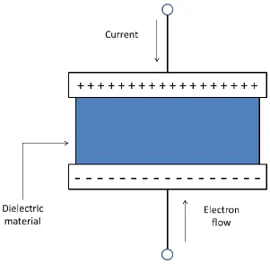
Traditionally current is described as the flow of positive charge, which is induced by the flow of electrons in the opposite direction. To illustrate how electrons interact with the capacitor as current flows through it, Figure 2 has been provided. Consider that electrons flow upwards into the capacitor; thus, a
4 | P a g e
Figure 2, Current Flowing Through A Capacitor
[Image created by Author]
Firstly as electrons accumulate on one capacitor plate and vacate the other; a voltage difference emerges across the capacitor. Also, simultaneously, current will flow as there is electron movement in progress. Capacitors are used to store charge, as charge can be stored on one plate. However the negative charge on one plate is always equal to the positive charge on the other; consequently the total net charge on both plates is zero. [1]
2.2.1 Pressure Tank Analogy
5 | P a g e
Figure 3, Capacitor Analogy with Pressure Tank
[Image created by Author]
2.2.2 Voltage And Stored Charge Relationship
The relationship between charge and voltage of an ideal capacitor is:
q = Cv (1)
Equation 1, Ideal Capacitor Voltage Charge Relationship
That is, the charge stored, in units of Coulombs, is directly proportional to the voltage across the
capacitive plates. The proportionality constant is called the capacitance C. Furthermore it is measured in Farads, a unit of measurement that describes how many Coulombs are stored per Volt. For most typical applications a Farad is considered to be an excessively high amount of capacitance. The general range of capacitance used in most electronic applications is from a few picoFarads to 0.01 Farad. [1]
2.2.3 Current And Voltage Relationship
For a capacitor the relationship between voltage and current is:
(2)
Equation 2, Capacitor Voltage Current Relationship
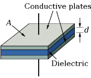
6 | P a g e 2.2.4 Characteristics Of Parallel Plated Capacitors
Figure 4 below shows the dimensions of a parallel plate capacitor. Each rectangular plate has an area A (W×L), a width W, and a length L. Between the plate pair is a distance denoted as d, that is occupied with a dielectric insulator. Provided both the length and width of the plates are much larger than the distance between them the capacitance can be approximated by:
(3)
Equation 3, Parallel Plate Capacitor Equation
[1]
The dielectric constant is denoted by . The dielectric constant is different for each material as indicated in Table 1.
Figure 4, Parallel Plate Capacitor Dimensions
[Image created by Author]
Material Relative Dielectric Constant r Dielectric Constant r× 0
Air 1 0=8.85× F/m
Diamond 5.5 4.87× F/m
Mica 7 6.20× F/m
Polyester 3.4 3.01× F/m
Quartz 4.3 3.81× F/m
Silicon dioxide 3.9 3.45× F/m
Distilled Water 78.5 6.95× F/m
7 | P a g e
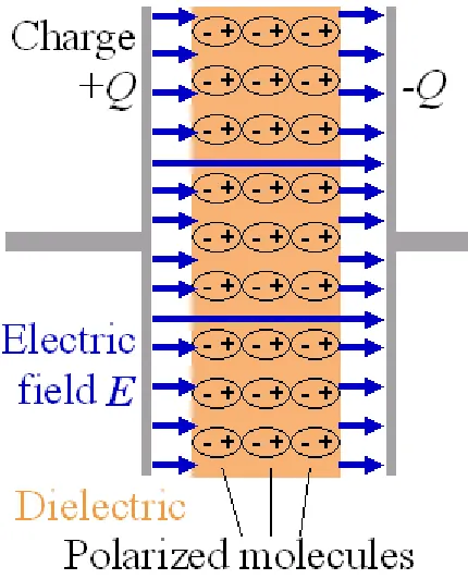
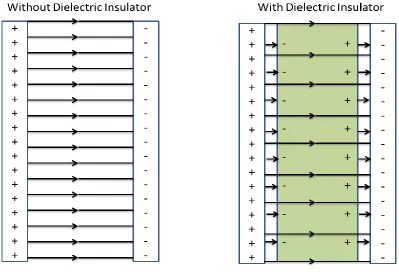
The dielectric insulator works because the molecules within the dielectric medium exhibit an electric field in the opposite direction. This effect occurs because of the charges on the plates. The dielectric produces the electric field because of the electric dipole moments of the molecules within the dielectric.
When a dielectric insulator is placed within a charged capacitor its molecules become polarized such that the net dipole moment is in parallel with the electric field. For instance if the molecules are polar (initially random orientation) they are aligned because of the torque induced by the field. If the molecules are non-polar, they are induced to be parallel to the field. In both cases the dielectric becomes polarized as indicated in Figure 5. [3]
Figure 5, Molecules In External Electric Field
[4]
8 | P a g e
Figure 6, Electric Field With/Without Insulator
[Image created by Author]
2.2.5 Parasitic Effects
Capacitors in the real world cannot always be modeled exclusively with just a capacitance. A real-world model circuit for a capacitor is provided in Figure 7. The series inductance Ls occurs because any current
that flows into the capacitor generates a magnetic field. The series resistance Rs occurs because there is
resistivity in the materials used in the capacitive plates. Lastly, there are no insulating materials that act as a perfect insulator; consequently, there is a resistance through the dielectric represented by Rp. Rs, Rp
and Ls are parasitic elements and they are always present in some degree. In circuit design care must be
9 | P a g e
Figure 7, Capacitor Including Parasitic Elements
Adapted from [5]
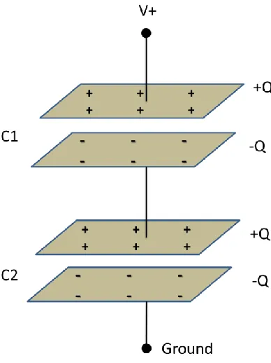
2.2.6 Capacitor Orientations And Charge
Figure 8 shows two capacitors that are connected in series. The charge across the first capacitor (C 1) is equal to the charge across the second capacitor (regardless of its capacitance) and the charge across both capacitors. This is because when the charge +Q appears on the first plate (from the positive terminal) the electric field from that charge induces an equal negative (-Q) charge on the inner plates of C1. To achieve this, electrons are withdrawn from the first plate of the second capacitor, while
10 | P a g e
Figure 8, Charge And Series Capacitors Relationship
[Image created by Author]
2.3 Capacitive Sensing Circuits
2.3.1 Oscillators
Many electronic instruments have an oscillator or waveform generator of some sort. A typical oscillator is required for any instrument that functions periodically, or initiates functions, or employs periodic waveforms for cyclical measurement. For instance oscillators are used in every computer peripheral from discs, printers and tapes. They are used in almost all digital instruments such as computers, oscilloscopes, digital multimeters, receivers, calculators, counters, timers. Usually a device absent of an oscillator is a slave and only operates when polled by a master device (that typically contains an
11 | P a g e
2.3.1.1 Relaxation Oscillators
One of the simplest types of oscillators is made by charging a capacitor through an RC circuit. After the capacitor reaches a threshold voltage limit it is quickly discharged. This is accomplished as the external circuit reverses the polarity causing the capacitor to discharge as well as changing the current direction when the threshold is reached. Typically the capacitor generates a triangle wave rather than a sawtooth wave (the latter occurs when capacitor discharges to ground). Relaxation oscillators are based upon this principle.
Relaxation oscillators have historically been constructed with negative-resistance devices like neon bulbs or uni-junction transistors. Modern practices however favor both special IC timers and operational amplifiers. Figure 9 below illustrates a commonly used RC relaxation oscillator. [6]
Figure 9 , Operational Amplifier Relaxation Oscillator
Adapted from [7]
The operation of this circuit is straightforward and based on the popular Schmitt trigger circuit. [6] By assuming the operational amplifier output is initially in positive saturation mode (the inverting terminal is charging to half V+); the capacitor charges up until it reaches half of V+ with an RC time constant of
12 | P a g e
2.3.1.2 CMOS Inverter Oscillator
Oscillators that use CMOS inverters can have a distinct advantage of having very low noise content or low side noise. Figure 10, illustrates a simple circuit that shares this desirable quality. A pair of CMOS inverters (typically used for digital logic) are connected in series to form an RC relaxation oscillator. As well as producing low noise qualities, even at higher frequencies (i.e 100 kHz) it also has the added advantage of outputting a squarewave at digital logic voltages. [6]
Figure 10, CMOS Inverter Oscillator
[Image created by Author]
2.3.2 Sensing Capacitance Using A Microcontroller
2.3.2.1 Astable Multivibrator Using A Microcontroller
Figure 11 is an astable multivibrator circuit that uses a microcontroller. This simple circuit has a microcontroller that calculates the capacitance through a frequency determining component of the astable multivibrator. The capacitance, Cx is to be measured by repeatedly charging and discharging the
13 | P a g e
Figure 11, Microcontroller-Astable Multivibrator
[Image created by Author]
While this setup is good at measuring larger capacitances, it is not very good at measuring capacitances in the lower picoFarads range. The lower the capacitance, the higher the output frequency for a fixed R, as capacitance is what determines an RC time constant. Under these circumstances, to keep frequencies slow enough when monitoring capacitors in the picoFarads range with a micro controller, the resistance needs to be increased to the mega Ohms region. However increasing the resistance to this range will jeopardise reliability of capacitive measurements because of the internal input resistance at pin B, which is rated at 100 MΩ. Moreover say R is also 100 MΩ; when Pin A is high, the impedance from pin B is in parallel with the capacitor. When Pin A is low, Pin B is in parallel with R, draining the capacitor with an equivalent 50 MΩ Circuit, which again jeopardises the reliability of the frequency and calculated capacitive measurement. [8]
2.3.2.2 QTouch
The QTouch technique uses a charge transfer scheme, with a setup shown in Figure 12. Here, the charge from the small capacitor, Cx is incrementally stored into the large capacitor, CL. As indicated in Figure 12,
there are very few components required to create this circuitry. In comparison with Figure 11, only an extra capacitor is required to replace the existing resistor.
The small capacitor Cx is cyclically charged and then discharged into the larger capacitor CL, until the
14 | P a g e
number of charge cycles completed. Finally all capacitors are discharged so that the process can begin again. The QTouch system uses the number of counts to identify any changes in the capacitance of Cx.
Because QTouch measures the summation of charge over a number of intervals; it is a technique that has an added benefit of being reasonably immune to interfering signals. For further information refer to Figure 12. [8]
Figure 12, QTouch Technique
Pseudo Code from [9]
15 | P a g e
Chapter 3 Approach
3.1 Chapter Overview
In the previous chapters, key objectives for the design of a total capacitance measurement system for water level sensing were described, and four existing capacitance sensing circuits were explored for inclusion in this system. This chapter presents a design overview for the total capacitance measurement system and the selection of peripheral components, based on these objectives. Finally, out of the four sensing circuits that were explored, the QTouch technique was selected for use, and the relevance of its benefits and limitations to this project are explained.
3.2 Peripheral Design Overview
Figure 13 below illustrates the design overview that combines key and peripheral objectives discussed in chapter 1. Each component has been selected for a unique reason that will be discussed in the following ‘3.3 Selection’ section.
Figure 13, Peripheral Design Overview
16 | P a g e
3.3 Peripheral Selection
3.3.1 Eleven Microcontroller
The Eleven microcontroller board, shown in Figure 14, was selected because it was compatible with the Arduino development environment. This development environment has an extensive range of libraries that allow easy control of Arduino-compatible components, such as the Arduino LCD shield and the MCP4725 DAC. The Eleven is 100% compatible with and is based on the existing Arduino Uno board [9]. The ICSP, headers and power jack are in identical locations to the Arduino Uno; enabling full
compatibility for all Arduino projects, sketches and shields. [9] The specifications of the Eleven microcontroller are given in 3.3.1.1 Specifications.
3.3.1.1 Specifications
MCU Type Atmel ATMega328P Input Voltage 7-12 V DC
Maximum Input Voltage Range
6-20 V DC
Operating Voltage 5 V
Digital I/O Pins 14 (with 6 able to provide PWM output) Analogue Input Pins 6 (also has digital I/O pin functionality) Analog Resolution 10 bits
Current Per I/O Pin 40 mA Total Current For All
I/O Pins
200 mA
Flash Memory 32 kB, with less than 1 kB occupied for Boot Loader. SRAM, EEPROM 2 kB SRAM, 1 kB EEPROM
Serial 1 x hardware USART, SPI (Serial Peripheral Interface), I2C
17 | P a g e
Figure 14, Freetronics Eleven Board
3.3.1.2 Arduino Development Environment
The Arduino development environment controls any Arduino or Arduino-compatible microcontroller. Software written within the Arduino development environment are called sketches. Sketches can be managed with the typical Libraries, C files (.c), header files (.h) and C++ files (.cpp). Sketches are written in the text editor. To assist debugging within the Arduino environment there is also a message area toolbar with common functions (i.e. verify/upload) and a serial monitor with a text console. Arduino is an electronic prototyping platform that utilises easy-to-use and flexible hardware/software. The Eleven microcontroller platform was selected because it is 100% compatible with the Arduino development environment and relatively affordable compared to other platforms. [10]
3.3.2 Freetronics LCD Display
18 | P a g e
Figure 15, Freetronics LCD Display
3.3.3 MCP4725 12-bit DAC
The MCP4725 12-bit breakout board, shown in Figure 16, is used to output a variable voltage between 0 to 5 volts. The output voltage is controlled via I2C that allows the microcontroller to signal the desired output voltage. I2C is a communication protocol that transmits data over two wires. The breakout board also has an EEPROM so that any output voltages can be restored if the device is power cycled. In total the breakout board has 6 pins: the supply voltage, ground, I2C address, voltage out, and both an SCL pin and SDA pin to facilitate I2C Communication. The I2C address pin is left completely unconnected since the default hex address 0x62 is used. [12]
19 | P a g e
Figure 16, MCP4725 12-bit Break Outboard
3.3.4 Analogue Voltage To Current Circuit
In an industrial setting DC signals can be used to represent physical measurements such as motion, pressure, flow, temperature and weight. Typically a DC current is preferenced over a DC voltage signal. A DC voltage signal circuit varies when there is a change of resistance across a signalling wire, because of resistive power losses. A DC current signal circuit, however, will transmit a constant current across a circuit regardless of any changes in resistance. Also, current sensing instruments usually use lower impedances to reduce power consumption, and noise immunity for current sensing instruments is significantly improved compared to that of DC voltage signals. [13]
20 | P a g e
[Image created by Author]
Figure 17, Transconductance Amplifier
Figure 17 illustrates the circuit diagram of a transconductance amplifier. The transconductance is
measured in Siemens and is the measure of ‘change in current divided by change in voltage’ (ΔI/ΔV). The transconductance ratio is made constant by the 250 Ω resistor resulting in a linear ‘voltage in’ to
‘current out’ relationship. Moreover an input voltage range of 1-5V linearly corresponds to an output current range of 4-20mA. [13]
3.4 Primary Selection
3.4.1 Conclusion And Choice For Capacitive Sensing
As discussed in Section ‘1.2 Objectives’ the key objectives in regards to the capacitive level sensing circuitry are to seek to optimise the following:
Accuracy
Disturbance rejection
Noise rejection
Sampling rate
Economical operations
Construction cost
21 | P a g e
3.4.1.1 Accuracy
The charge transfer QTouch system was selected because; out of all the researched capacitive sensing circuits it satisfied the most objectives. As the QTouch system is designed for detecting finger proximity it has typically not been concerned with measuring actual capacitance values, such as a relaxation oscillator used in a digital multimeter. Leakage (that is measured in charge per second or amps) that exists within all electrical components from dielectrics to transistors/MOSFETs will undermine the accuracy of the QTouch system, as it samples accumulated charge. In short, the alternative proposed designs, such as the oscillators are better at detecting actual capacitance; however, the QTouch system is very good at detecting changes in capacitance. For the purpose of developing a level sensor, the detection of changes in capacitance within a set range aligns with this project.
3.4.1.1.1 Law of Large Numbers
The Law of Large Numbers is typically a justification for assuming statistical normality. It says that any average set of independent random variables will converge to the mean as the number of samples increase. For instance, when flipping a coin four times and the results may yield 75% heads and 25% tales; however, if the number of coin flips were to approach infinity the results will always converge towards its true mean of 50-50. Moreover the mean of heads will approach 0.5. [14]
3.4.1.2 Noise And Disturbance Rejection
For the application of detecting the liquid level within a tank, the types of noises or disturbances that are undesirable are small fluctuations caused by electromagnetic interference (EMI) or slower
fluctuation caused by rippling waves on the water’s surface [15]. It is therefore desirable that a system that can filter out ‘sudden pulses’. The procedure behind the QTouch system is that for each ‘capacitive sense operation’ there is a small amount of corresponding charge stored into the larger capacitor. A voltage threshold for the larger capacitor is set so that when it is met, the microcontroller counts the number of cycles required. The microcontroller then uses this information to perform an averaging calculation. The threshold voltage indicates the total charge stored and ‘the number of cycles’ indicates how many ‘sets of charge’ were required. This information allows the microcontroller to perform a ‘summation of charge’ divided by the ‘sets of charge’ averaging function, that will reduce undesired noise and disturbances being sensed. Note that one ‘set of charge’ can be considered equivalent to the ‘Count’ variable in both Figure 23 and Figure 12 pseudo code.
3.4.1.3 Economic And Construction Costs
The bulk of the materials cost of the QTouch system is in the microcontroller. Arduino-clone microcontrollers can be priced as low as $10 on eBay. The rest of the circuitry is just the cost of the associated wires, two 150 ohm resistors and the reference capacitor. The circuitry can be adapted to increase sampling rate at the expense of increased power consumption, or the power consumption can be decreased along with the sampling rate. Methods of decreasing power consumption and methods to increase sampling rate are explored later in section ‘7.1 Future Work’. The QTouch system may
22 | P a g e 3.4.2 QTouch Background
The QTouch proximity sensor, patented in 2011 was invented by both Harold Phillips and Kevin Snoad [16]. It is a capacitive charge transfer based proximity sensor that includes a sensing element and a known reference capacitor. This invention exclusively relates to proximity sensing, which is an high demand function as human interfaces are increasingly leaning towards capacitive over mechanical touch sensing. In the interfaces of everyday appliances such as phones, MP3 players and some modern panels it is typical to find plastic panels or glass with a capacitive touch control system behind. [16]
The current QTouch system is designed for detecting objects such as fingers. Detecting the presence of a finger is not as simple as typically there is only a very small capacitance in the order of a few picoFarads ( Farads). Furthermore this infinitesimal change in capacitance, for many systems, needs to be detected upon an existing background capacitance in the order of tens of nanoFarads. This is where the technology of the QTouch charge transfer excels. QTouch has been shown to sense in the most
challenging environments as it mandates a high signal to noise ratio (SNR). [17]
3.4.3 Further QTouch Development Requirements
The QTouch proximity sensor circuit as it stands infers the capacitance through counting the amount of completed charge cycles. The design does not directly measure capacitance. For a capacitor level sensor it is preferable to measure the capacitance directly; because from Equation 3 in Section ’2.2.4
Characteristics Of Parallel Plated Capacitors’, the capacitance will be directly proportional to the water level. In this equation, the area and distance between the plates remains constant while the dielectric ratio of ‘air to water’ varies; thus causing the capacitance to be directly proportional to the ‘dielectric ratio’ and through it the water level. Therefore, further changes to the QTouch system are required to create a capacitive meter.
The solution may rest in a physics problem from a textbook [3]. There is an example problem where two capacitors connected in series, 6 µF and 12 µF, each initially uncharged experience a 12 V voltage difference induced by a battery, refer to Figure 18.
Figure 18, Series Capacitors, Charge and Voltage
23 | P a g e
The voltage between the capacitors is calculated by noting that the charge that goes through the first capacitor also must pass through the second. Also a traditional KVL voltage loop is used to identify that the voltage across the first capacitor and the second must equal the supply voltage. Therefore the equations that describe Figure 18 are the following:
(4)
Equation 4, KVL Series Capacitors
Letting C1 and C2 be the capacitance across V1 and V2 respectively. Also by using Equation 1, and noting
that the charge across each capacitor must be equal:
(5)
Equation 5, Equivalent Charge
24 | P a g e
Chapter 4 Assumptions
4.1 Chapter Overview
This chapter highlights some of the common assumptions made in electronic design, all of which fall under the “ideal circuit” concept, such as perfect operation of circuit elements and absence of parasitic effects. The effect of assuming an infinite impedance state for input pins in the QTouch circuit is also discussed. These assumptions are then assessed and compensatory measures discussed.
4.2 Common Assumptions
In electronic system design it is common to use ideal circuit concepts or assumptions. These include ideal operations of a perfect ground, the perfect amplifier, the perfect voltage or current supply and no parasitic effects for all circuit components. Also in the context of the microcontroller, assuming infinite impedance for input pins and zero impedance for output pins is another example.
In reality these perfect circuit elements do not exist. For instance a perfect ideal voltage source would have zero impedance and would be able to maintain voltage supply across any load no matter what current is required. For an ideal voltage source, as the resistance applied across it is reduced towards 0 Ω both the current and power required to maintain voltage would be increased towards infinity. Furthermore suppose that a 5 V supply was to deliver a current of 2 A, if the voltage supply drops from 5.001 to 4.999 V the voltage source must have an internal impedance of approximately one milliohm. [18]
One of the more unreliable suppositions that may undermine the accuracy of the QTouch sensor is assuming an infinite impedance state for pins that are configured as inputs. In reality, because capacitors are being charged up and left at static voltage levels, a very small amount of leakage will undermine the capacitor’s expected ideal voltage levels. This may adversely affect the solving of any ideal equations that use voltage levels across capacitors. Furthermore because input pins produce a high impedance state, with nothing connected to them they may experience random changes in the form of the surrounding environment’s electrical noise or capacitive coupling produced by nearby electronics (i.e. such as other pins). [19]
4.3 Assessing the Assumptions
25 | P a g e
26 | P a g e
Chapter 5 Methodology
5.1 Chapter Overview
In previous chapters, the benefits and limitations of using QTouch for capacitance sensing in a water level sensor were presented and discussed. Specifically, in 3.4.3 Further QTouch Development
Requirements, the approach taken to adapting the QTouch technology to meet the requirements of the water level sensor was introduced, namely, to enable it to directly measure capacitance. In this chapter, this approach is expanded upon in a mathematical investigation showing how the relationship between iterated measurements of voltage and capacitance can enable the QTouch to measure capacitance using the relationship equation. Next, circuit design for the water level sensor is discussed, and two designs for the system are proposed. The final section in this chapter follows construction of the water elvel sensing probes.
5.2 Evolving QTouch Into A Capacitance Meter: A Mathematical Investigation
5.2.1 Introduction
To develop the existing QTouch system into a capacitance meter a mathematical analysis of the system is required. There is little information available in most textbooks about the behavior of capacitors in series when there is charge initially stored in either capacitor. It is therefore important that a series of mathematical investigations and/or simulations are required to map initial voltage and capacitance relationships. These circuit simulations are run in Intusoft ICAP/4 Spice software package [20].
5.2.2 Investigation Objectives
The QTouch method cyclically charges the second capacitor into the first capacitor for a limited amount of times, and then afterwards grounds both capacitors before continuing further cyclical charge
27 | P a g e 5.2.3 Investigation
To replicate the QTouch charging process a Spice (ICAP) simulation was performed based on a model using ideal equations. A capacitor of 10 nF was put in series with a 1 nF capacitor as shown in Figure 19.
Figure 19, QTouch Simulation
Initially the spice simulation was run with a voltage of 100 V applied across both capacitors. The initial voltages for both the capacitors where set to 0. After the simulation was run, the’ transient response’ of the voltage at node 2 (voltage across C2) was graphed and the steady state voltage was computed as 90.909 volts. To parallel the QTouch technique described in section ‘2.2.2.2 QTouch’, the steady state voltage (at node 2) of the first Spice simulation (90.901 volts) was used to calculate the initial voltage of capacitor C1 for the next iterative simulation. Moreover, to achieve this initial voltage at node 2, the initial condition across C1 was set to ‘node 2 voltage subtract the supply voltage’ or 9.09 volts, see Figure 20. The simulation was again run and the second steady-state response at node 2 was 82.644 Volts. This action of observing the voltage at node 2, to use it for the initial voltage of the next simulation was carried out 10 times. The results are tabled below in Figure 21 and Table 2.
28 | P a g e
Figure 20, QTouch Spice Simulation Initial Condition
29 | P a g e
Voltage (V) @ Node 2
Simulation Iteration 90.9091 1 82.6446 2 75.1315 3 68.3013 4 62.0921 5 56.4474 6 51.3158 7 46.6507 8 42.4098 9 38.5543 10
Table 2, QTouch Voltage Per Iteration
5.2.3.1 Iteration One
Both capacitors in series will have no initial voltage across them when the 100 V is applied. As such the total charge across the first capacitor is going to be equal to the total charge across the second
capacitor. It is therefore that Equation 4 and Equation 5 maybe combined to solve for the voltage at node 2.
( )
( )
This calculated result is the same result produced from the first iteration of the spice simulation.
5.2.3.2 Other Iterations
In the second simulation iteration, C1 had an initial voltage of 9.0909 volts. All the charge that goes
through the first capacitor must also go through the second capacitor, regardless of the initial voltage across C1. However, according to Kirchhoff’s voltage law, one must now consider the initial voltage
across C1 as it is a part of the loop. Consequently the new equation is as follows:
( ) ( )
( )
Through defining as (n) - (n-1) both these equations may be rewritten as:
( ) ( ) (6)
Equation 6, KVL With Initial Conditions
( ( ) ( )) (7)
30 | P a g e
Through equating Equation 6 and Equation 7 the combined equation is:
( ( ) ( )) ( ( )) (8)
Equation 8, Both Equations 6 And 7 Combined
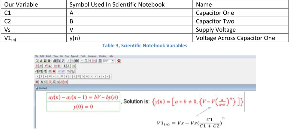
Later in this section a recursive solution for Equation 8 will be obtained, as there are further advantages, later discussed. For now the mathematics program ’scientific notebook’ by Mackichan Software Inc [21], will be employed to provide the recursive solution for Equation 8 and will later be used to compare with our calculated solution. To allow ‘Scientific Notebook’ to compute Equation 8 we replace our variables with one letter symbols, see Table 3. For instance:
Our Variable Symbol Used In Scientific Notebook Name
C1 A Capacitor One
C2 B Capacitor Two
Vs V Supply Voltage
V1(n) y(n) Voltage Across Capacitor One
Table 3, Scientific Notebook Variables
Figure 22, Scientific Notebook Recursive Solution
By taking the recursive solution from Figure 22 and substituting V1(n) with ‘Vs – V2(n)’ (in accordance with
KVL) the resulting solution is:
( ) ( ) (9)
Equation 9, Recursive Solution For 'Node 2' Voltage
Where V2(n) is the voltage at node 2.
31 | P a g e
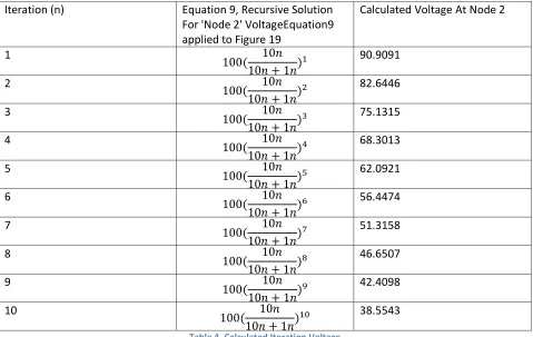
Iteration (n) Equation 9, Recursive Solution For 'Node 2' VoltageEquation9 applied to Figure 19
Calculated Voltage At Node 2
1 (
)
90.9091
2 (
)
82.6446
3 (
)
75.1315
4 (
)
68.3013
5 (
)
62.0921
6 (
)
56.4474
7 (
)
51.3158
8 (
)
46.6507
9 (
)
42.4098
10 (
)
38.5543
Table 4, Calculated Iteration Voltage
The calculated results from Equation 9 of Table 4 are the same results that were computed from the Spice simulation in Table 2.
5.2.3.3 Solving/Enhancing The Recursive Formula
By Using Equation 8 and substituting V1(n) with ‘Vs-V2(n)’ or V1(n-1) with ‘Vs-V2(n-1)’ as in accordance with
KVL, we get:
( ( ) ( )) ( ) (10)
Equation 10, QTouch Recursive Formula At Node 2
The simplification involving cancelling out the supply voltages in Equation 10assumes that the supply voltage will remain constant throughout iteration cycles. By taking Equation 10 and adding 1 to each ‘n’ term the equation becomes:
( ( ) ( )) ( ) (11)
32 | P a g e
By equating both Equation 11 and Equation 10 through the common V2(n) term:
( ) ( ( )) ( ) ( )
To again substitute Equation 11 a second time the resulting equation would be:
( ) ( ( )) ( ) ( )
The pattern that emerges from this series of consistent substitution is the following:
( ) ( ) ( ) (12)
Equation 12, The Recursive Moving Average Equation
Notice how this equation will allow us to solve for C2 using any two voltage iterations sampled from the QTouch’s cyclical measurements. Moreover if we set x to equal n and assumed that V2(0) is equal to the
supply voltage
( ( ) ( ) ) ( )
And assuming V2(0)=Vs
(
) ( )
Note how this is the same solution as Equation 9 that was computed by scientific notebook.
5.2.4 Investigation Conclusion
The investigation was successful in the sense that it was able to identify some significant mathematical relationships. Firstly Equation 9, allows the microcontroller to calculate a corresponding average capacitance over the course of consecutive charges from both any voltage detected at node 2 and by counting the number of charges executed. Secondly Equation 12 may be used to calculate a
corresponding moving average capacitance between two sampled voltages, at different iterations, at node 2. Finally both Equation 4and Equation 5 may be used to calculate a capacitance from a single charge and the voltage difference applied across both series capacitors.
33 | P a g e
5.3 Adapted QTouch Capacitance Meter Circuitry
5.3.1 The QTouchvs ‘QTouch Analogue’ Design
The analogue QTouch design is almost identical to the pre-existing QTouch proximity sensor. The only difference between the two is that the digital read pin is substituted with an analogue read pin. Also the pseudo code is changed to accommodate for this hardware difference (see Figure 23). While the
differences between ‘QTouch’ and ‘QTouch analogue’ are difficult to explain, a simplified water analogy can still illustrate key operations.
Figure 23, QTouch Analogue Design
[Image created by Author]
5.3.1.1 The QTouch Design Analogy
34 | P a g e
Figure 24, Qtouch Analogy
[Image created by Author]
5.3.1.2 QTouch Analogue Analogy
5.3.1.2.1 Equation 9
‘QTouch Analogue’ has two key equations that operate in slightly varying ways, Equation 9 behaving most similarly to the initial QTouch system. This equation operates identically with initial designs but with one difference. Rather than waiting for the system to reach a threshold voltage to calculate the capacitance; it senses the voltage level across the capacitor and calculates the average capacitance at any measurement.
35 | P a g e
Figure 25,QTouch Analogue Equation 9 Analogy
[Image created by Author]
5.3.1.2.2 Equation 12
Within the QTouch Analogue design, Equation 12 measures the unknown capacitance through detecting the difference between two voltages and counts the iterations between both samples. It is similar to Equation 9, only that it will calculate the capacitance from any reference voltage rather than just the initial supply voltage at the beginning of the cycle. Moreover Equation 12 calculates the capacitance from a recent change in voltage instead of the total change in voltage.
36 | P a g e
Figure 26, QTouch Analogue Equation 12 Analogy
[Image created by Author]
5.4 Single Charge Based Capacitance Meter Circuitry
5.4.1 Introduction
As previously discussed, Figure 18 and its applied Equation 5 can be used to create a type of capacitance meter that functions through using a reference capacitor. The Arduino UNO compatible or Eleven microcontroller boards have an analogue reference capability that allows the user to set the top input range of the 10 bit analogue input. For instance the default 0 to 5 V range can be altered to 0 to 2.5 V. [22] knowing this, the locations reference capacitor and measured capacitor must be selected.
As shown in Figure 27, the pin above C1 is switched between output high and low. The pin below C1 is
switched between an analogue input to output low (or ground). The high state can be assumed to be 5 V, as that is the operating voltage for Arduino Uno compatible boards. The sampling resolution and/or range of the analogue input pins will contribute to the accuracy of the capacitance measurement. The capacitance vs voltage (at pin B) relationship will also affect accuracy. Therefore the mathematical relationship between the voltage at pin B, and the allocation (at C1 or C2) of the unknown capacitance
37 | P a g e
Figure 27, Single Charge Based Capacitance Meter
[Image created by Author]
5.4.2 Investigation
The relationship between both capacitors and the voltage at pin B (V2) (Figure 27) can be mathematically
modeled by combining Equation 4 and Equation 5. Both these equations can be combined to form either the ratio of C1/C2, see Figure 28 or the ratio of C2/C1, see Figure 29.These equations and corresponding
38 | P a g e
Figure 28, C1 Vs C2 Ratio
39 | P a g e 5.4.3 Conclusion
It is more desirable to make C1 the unknown capacitance as the voltage-capacitance relationship will
mimic the behavior of the graph in Figure 28. This is desirable because the AREF Arduino IDE function [22] can set the analogue input pin with 10 bit resolution to sample a ‘0 to 2.5 V’ range. This is more preferable than the whole default ‘0 to 5 V’ range as it will focus on the more linear behaving section of the curve. The trade-off is that if C1is larger than C2 it will cause the voltage at pin B to exceed 2.5 V. It is
therefore important to ensure that C2 is always larger than C1.Figure 30 illustrates how closely the ‘0 to
2.5 V’ analogue input range is to a perfect linear equation.
Figure 30, C1/C2 Line Versus Linear Comparison
The nonlinearity of the C1/C2 ratio means that unlike the linear counterpart it will not share uniform accuracy across the whole range. For instance this line will give better resolution for smaller C1/C2 ratios at the expense of ratios that are closer to 1. As it is very close to a linear line it should still provide a highly reasonable 10 bit resolution across the 0 to 2.5 V range. Thus the final circuit diagram for the ‘Single Charge Based Capacitance Meter’ is indicated in Figure 31 .
0 0.2 0.4 0.6 0.8 1 1.2
0 0.5 1 1.5 2 2.5 3
C1/C2 Ratio
Linear y=x/2.5
C1/C2 C1/C2
40 | P a g e
Figure 31, Final Single Charge Circuit Diagram
[Image created by Author]
5.5 Construction
5.5.1 Introduction to Capacitive Plate Design
41 | P a g e 5.5.2 Capacitive Plate Design And Error Considerations
One of the most important aspects of a capacitor level sensor is the dielectric constant of the process material. It must be considered that the dielectric constant of the processing material may be
dependent on any internal change in temperature, humidity, moisture content and density. It is easier and more reliable to measure the level of process materials with a higher dielectric constant. Materials with a higher dielectric constant are ideal candidates for capacitive level measurement because they induce a pronounced and greater change in capacitance that is less likely to be mistaken for
environmental noise. In comparison, materials with low dielectric constants such as sand, plastics and glass do not make great candidates for capacitive measurement applications.
Sensitivity of a parallel capacitive probe can be increased in two ways, by decreasing the distance between or by increasing the area of the coupled plates. It is important that the plates are close together but also not too close so the processing material does not get trapped between them or be prevented from flowing freely. High viscosity, wet and sticky materials may cause coating or permanent build up within the probes and cause level measurement errors.
In the case of a water level sensor, as the water level drops the probes could remain wet resulting in a water-air dielectric insulation combination. A quicker fall in water level results in larger false readings of level measurements. It is also important to ensure that capacitive plates are well insulated, to prevent the water, which is highly conductive due to dissolved ions, from short-circuiting between electrodes.
5.5.3 Capacitive Plate Construction
42 | P a g e
Figure 32, Initial Capacitive Probe Construction
Two coats of Electrical insulation varnish (also known as ‘ULTIMEG 2000 372’) were used to cover both capacitive electrodes. This approach was not successful in that microscopic spots were left uncovered, and enabled the water to conduct electricity through the plates. Also both plates would easily obtain small scrapes when their edges and corners touched other objects, such as the ground. Because the capacitive plates were not properly electrically insulated, the acrylic plastic that was used to separate the plates had to be destroyed. This allowed for further attempts to re-insulate both capacitive plates.
To ensure both capacitor probes were electrically insulated they were taken to a facility run by ‘Global Rewinds Pty Ltd’, a company that makes and sells customized motors. At the facility there was a varnishing pool and a large 12.5 tonne varnishing oven, traditionally used to insulate internal motor coils. Both capacitive plates were dipped in this varnishing pool and then afterwards left in the varnishing oven for three hours.
Even capacitive plates need shoes right?
The bottom corners of the plates were most susceptible to high-pressure contact with other objects that would result in small scratches that would prevent proper insulation. To prevent scratches from
43 | P a g e
Figure 33, The Capacitor Plates Preparation For Rubber Boots
After the rubber coating was applied, duct tape was used to wrap the rubber coating to further protect against any potential knocks (see Figure 34). Finally a rubber coating (Figure 35) was applied across the whole capacitive probe. The rubber coating is designed to prevent the insulating varnish from being scratched, as the rubber helps distribute the force from foreign objects and maintain insulating integrity. To separate the electrodes, square plastic, toothpicks-sized blocks were placed against a capacitive plate and wrapped up with a single plate in electrical insulation tape (Figure 36). Finally the coupled
electrodes were held together by rubber bands (Figure 37).
44 | P a g e
Figure 35, Leak Seal Used For Rubber Coating
45 | P a g e
Figure 37, Capacitive Probes Held Together With Rubber Bands
5.5.5 Conclusion
The capacitive probes have a submergible length of 1.05 m and a width of 5 cm and a coupled spacing distance of 2 mm. The rubber coating along the plates was applied equally; however the extra
46 | P a g e
Chapter 6 Results
6.1 Chapter Overview
Following on from the methodology and design discussed in Chapter 5, this chapter presents the results of three experiments. The first experiment compared the measured capacitance of different capacitors as taken by a high-accuracy digital multimeter, the QTouch Analogue Circuit and the Single Charge Circuit. This compared the accuracy of the three technologies. In the second experiment, capacitor probes were used in the developed water level sensor, utilising the QTouch Analogue Circuit, to measure the water level of a tank, to test the relationship between measured capacitance and water level.
6.2 Experiment 1
In Table 6 a range of ceramic capacitors from 1.8 pF to 10 nF were measured with a high-accuracy digital multimeter Q1156, the Single Charge circuit, (discussed in 5.3 Single Charge Based Capacitance Meter Circuitry) and the QTouch Analogue Circuit (discussed in 5.2 Adapted QTouch Capacitance Meter Circuitry). The rated tolerance across the set of ceramic capacitance was ±10%. The rated accuracy for the Q1156 DMM, is indicated in Table 5 below and also is included in the appendix. It is also important to note that alligator probes are used, which could easily induce a further measurement error on account of the capacitance induced from the probes.
Table 5, DMM Q1156 Accuracy
For a 0 to 200 nF range the accuracy of the Q1156 DMM is defined by ±(1%+5d), where ‘d’ is the resolution. Therefore for measuring a 1.8 pF capacitor the multimeter has a rated uncertainty of ±(1.8pF×0.01+5×1pF) or ±5.018pF.
The experiment that produced the results in Table 6 was conducted in the following way. A set of ceramic capacitors with 10% tolerances were measured by the DMM Q1156, Single Charge Circuit and the QTouch Analogue Circuit. The goal of this experiment was to measure the change in capacitance as a ceramic capacitor was introduced to each measuring system. Both circuits measured a certain amount of picoFarads when there was no capacitor present. This amount was subtracted from the result of the measurement devices.
47 | P a g e
averaged then recorded. Both programs used for these experiments are provided in the appendices of this thesis.
Rated Ceramic Capacitance
DMM Q1156 Single Charge (14.39nF) No Tear
Analogue Qtouch (101.2nF) 0pF (capacitor removed) 10pF 23.5pF 54.5pF Rated Ceramic
Capacitance (with subtracted initial 0pF reading)
DMM Q1156 Change
Single Charge (14.39nF) Analogue Qtouch (101.2nF)
0pf (capacitor removed) 1pF 1.5pF -0.07pF
1.8pF 2pF 6.5pF 2.56pF
4.7pF 7pF 8.05pF 5.22pF
8.2pF 11pF 13pF 8.68pF
33pF 35pF 39.5pF 33.66pF
47pF 47pF 53.22pF 45.9pF
101pF 107pF 104.8pF 102.19pF
331pF 331pF 347pF 339pF
471pF 440pF 466.4pF 451pF
681pF 647pF 687pF 663pF
1nF 942pF 968pF 964pF
2.2nF 2.2nF 2352pF 2275pF
10nF 10.6nF 12856pF -
Table 6, Measured Capacitances
6.2.1 Discussion
From these results it appears that the analogue QTouch system is more correlated to the capacitor ratings than the single charge circuit. As the single charge circuit would typically read a slightly higher capacitance then both the competing capacitive measurement devices and the ratings for the ceramic capacitors. It is difficult to totally dismiss any measuring system here as the ceramic capacitors only have a ±10% tolerance. Also the Q1156 at small values is not reliable because 5d is more than 1%, refer to Table 5. Therefore it is reasonable to conclude that the actual capacitor value is not known in this experiment.
There are a few ways in which this experiment could have been improved. Firstly smaller alligator probes could have been used to reduce the capacitance caused by the parasitic effects upon the leads. Secondly upon reflection each capacitor may have been mixed up with another identically rated ceramic capacitor upon being retrieved for measurement. This could have induced a perceived error across the tolerance of the ceramic capacitors. Finally an additional DMM Q1156 could be used to create a dataset and identify any measurement outliers that may be produced.
6.3 Experiment 2
0-48 | P a g e
15.3nF range to better reflect the capacitance variation for the capacitor probes. In addition the single charge transfer circuit has been excluded from the experiment as it has not produced the same level of accuracy as the analogue QTouch circuit in experiment 1, as shown in Table 6.
Capacitor(pF) 10% An-QTouch (101.2nF) Within Rated Capacitance
No1.Q1156 Within Rated Capacitance
No2.Q1156 Within Rated Capacitance
1.8 1.99 FALSE 3 FALSE 4 FALSE
2.2 2.51 FALSE 3 FALSE 3 FALSE
4.7 4.9 TRUE 6 FALSE 7 FALSE
8.2 8.68 TRUE 9 TRUE 10 FALSE
33 33.5 TRUE 33 TRUE 34 TRUE
47 45.27 TRUE 46 TRUE 47 TRUE
82 83.1 TRUE 85 TRUE 86 TRUE
101 102.66 TRUE 104 TRUE 104 TRUE
151 150.33 TRUE 153 TRUE 151 TRUE
221 229.77 TRUE 225 TRUE 230 TRUE
331 332.6 TRUE 322 TRUE 330 TRUE
471 471.14 TRUE 463 TRUE 469 TRUE
681 662.01 TRUE 650 TRUE 660 TRUE
1000 954 TRUE 950 TRUE 997 TRUE
2220 2234 TRUE 2280 TRUE 2280 TRUE
2720 2626 TRUE 2620 TRUE 2670 TRUE
3920 4133 TRUE 4150 TRUE 4250 TRUE
6820 6663 TRUE 6660 TRUE 6760 TRUE
15300 14576 TRUE 14554 TRUE 14770 TRUE
Table 7, Measured Capacitance Treating Rated Capacitors As Oracle
6.3.1 Discussion
From these results it is impossible to determine which measuring system is more accurately measuring each capacitor. As Table 7 indicates almost all measurements are taken within the tolerance of the rated capacitors. The results cells that are filled in with colour are the measurements that exceed the
49 | P a g e
Capacitor(pF) 10% An-QTouch (101.2nF)
No1.Q1156 No2.Q1156
1.8 TRUE 1.99 TRUE 3 4 TRUE
2.2 TRUE 2.51 TRUE 3 3 TRUE
4.7 TRUE 4.9 TRUE 6 7 TRUE
8.2 TRUE 8.68 TRUE 9 10 TRUE
33 TRUE 33.5 TRUE 33 34 TRUE
47 TRUE 45.27 TRUE 46 47 TRUE
82 TRUE 83.1 TRUE 85 86 TRUE
101 TRUE 102.66 TRUE 104 104 TRUE 151 TRUE 150.33 TRUE 153 151 TRUE 221 TRUE 229.77 TRUE 225 230 TRUE
331 FALSE 332.6 FALSE 322 330 TRUE
471 TRUE 471.14 TRUE 463 469 TRUE
681 FALSE 662.01 FALSE 650 660 TRUE
1000 FALSE 954 TRUE 950 997 FALSE
2220 TRUE 2234 TRUE 2280 2280 TRUE
2720 FALSE 2626 TRUE 2620 2670 TRUE
3920 FALSE 4133 TRUE 4150 4250 FALSE
6820 FALSE 6663 TRUE 6660 6760 TRUE
15300 FALSE 14576 TRUE 14554 14770 FALSE
Table 8, No1.Q1156 As Oracle
Table 8, treats DMM No1.Q1156 as an Oracle (the DMM is assumed to read with 100% accuracy), and all the measurements or rated capacitance that exceed the rated accuracy of this meter are highlighted, refer to Table 5. The assumption of this table is that the true capacitance must be within the rated accuracy limits of the capacitance that are measured by “No1.Q1156”. If this assumption is correct it will mean that two measurements from the analogue QTouch device are incorrect and three
50 | P a g e
Capacitor(pF) 10% An-QTouch (101.2nF)
No1.Q1156 No2.Q1156
1.8 TRUE 1.99 TRUE 3 TRUE 4 2.2 TRUE 2.51 TRUE 3 TRUE 3 4.7 TRUE 4.9 TRUE 6 TRUE 7 8.2 TRUE 8.68 TRUE 9 TRUE 10 33 TRUE 33.5 TRUE 33 TRUE 34 47 TRUE 45.27 TRUE 46 TRUE 47 82 TRUE 83.1 TRUE 85 TRUE 86 101 TRUE 102.66 TRUE 104 TRUE 104 151 TRUE 150.33 TRUE 153 TRUE 151
221 FALSE 229.77 TRUE 225 TRUE 230
331 TRUE 332.6 TRUE 322 TRUE 330 471 TRUE 471.14 TRUE 463 TRUE 469
681 FALSE 662.01 TRUE 650 TRUE 660
1000 TRUE 954 FALSE 950 FALSE 997 2220 TRUE 2234 TRUE 2280 TRUE 2280 2720 TRUE 2626 TRUE 2620 TRUE 2670
3920 FALSE 4133 FALSE 4150 FALSE 4250 6820 TRUE 6663 TRUE 6660 TRUE 6760
15300 FALSE 14576 TRUE 14554 FALSE 14770
Table 9, No2.Q1156As Oracle
Table 9, assumes DMM No2.Q1156 as an Oracle. If this assumption is correct it would again indicate that two measurements of the analogue QTouch system are incorrect and three measurements from