COMPUTER SCIENCE & TECHNOLOGY
www.computerscijournal.org
March 2017, Vol. 10, No. (1): Pgs. 86-93 An International Open Free Access, Peer Reviewed Research Journal
Published By: Oriental Scientific Publishing Co., India.
A New 8T SRAM Circuit with Low Leakage and High Data
Stability Idle Mode at 70nm Technology
P. RAIkwAL
1*, V.NEEMA
1and A.VERMA
21Department of Electronics and Telecommunication Engineering,
IET, Devi Ahilya University, Indore, India.
2Department of Electronics and Instrumentation Engineering,
IET, Devi Ahilya University, Indore, India. *Corresponding author E-mail: [email protected]
http://dx.doi.org/10.13005/ojcst/10.01.12
(Received: February 16, 2017; Accepted: March 10, 2017)
AbSTRACT
Memory has been facing several problems in which the leakage current is the most severe. Many techniques have been proposed to withstand leakage control such as power gating and ground gating. In this paper a new 8T SRAM cell, which adopts a single bit line scheme has been proposed to limit the leakage current as well as to gain high hold static noise margin. The proposed cell with low threshold voltage, high threshold voltage and dual threshold voltage are used to effectively reduce leakage current, and delay. Additionally, the comparison has been performed between conventional 6T SRAM cell and the new 8T SRAM cell. The proposed circuit consumes 671.22 pA leakage current during idle state of the circuit which is very less as compare to conventional 6T SRAM cell with sleep and hold transistors and with different b ratio. The proposed new 8T SRAM cell shows highest noise immunity 0.329mv during hold state. Furthermore, the proposed new 8T SRAM circuit represents minimum read and write access delays 114.13ps and 38.56ps respectively as compare to conventional 6T SRAM cell with different threshold voltages and b ratio.
keywords: SRAM, static noise margin, single bit line, threshold voltage, leakage current, b ratio.
INTRODUCTION
It has always been a great challenge to fabricate a circuit using transistors. To design a big circuit the size of transistor is becoming small1.
SRAM utilizes minimum sized transistors to fulfill the requirement of high packing density. SRAM is facing severe difficulties after scaling the dimensions of transistor, such as degraded data stability and increased power consumption at advanced
technology nodes 2. The dynamic power dissipation
can be reduced by supply voltage scaling 3,4. But
scaling the supply voltage has adverse effect on static noise margin 5. So to improve throughout
performance of the SRAM cell is a great challenge for the designers 6.
idle mode7. MTCMOS and power and ground gating
are the most widely utilized circuit techniques for suppressing the leakage current8,9. In this paper
a new single ended 8T SRAM is explored. The proposed cell utilizes an extra transistor (CS) to disconnect the feedback loop during active mode. A new read circuitry is introduced to read the stored content.
Previously proposed Conventional 6T SRAM cell with ground gated technique
Already published ground gated technique is reviewed in this part of the paper. Fig.2 shows conventional 6T SRAM cell with ground gated circuit. Fig.1 presents the conventional 6T SRAM cell. As conventional 6T SRAM cell is not reliable to perform the operation at low voltage because of voltage division between the access transistors and the pull-down transistors in cross coupled inverters 10. That affects the data stability of the cell.
Therefore, the widths of the pull down transistors are changed to improve the data stability as well as for low power dissipation. The ratio of w/L ratio of pull up transistor to the w/L ratio of pull down transistor is known as beta ratio (b) 11.
In ground gated 6T SRAM circuit a high threshold PMOS hold (HLD) transistor is connected in parallel with high threshold NMOS sleep (SLP) transistor shown in fig.2. This circuitry is connected between the memory cell and ground12. During
the active mode sleep transistor (N_5) is kept ON while hold transistor (P_3) is OFF. That maintains the ground level approximately at 0 volts. During the idle mode sleep transistor is off whereas hold is on13. This particular state of the sleep and hold
transistors suppress the leakage current when the circuit is in idle mode11,14. In sleep mode the on state
of the hold transistor helps to preserve the stored content of the cell 15.
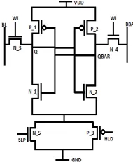
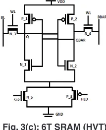
The transistors sizes are in nanometer 70nm CMOS technology. wL represents wordline, BL and BBAR represent bitline and bitline bar respectively. Fig. 3(a) represents ground gated 6T SRAM cell using low threshold voltage transistors (LVT), where analysis has been performed for b=1 and b=3. SLP and HLD utilize high threshold voltage transistors. Fig. 3(b) represents ground gated 6T SRAM cell using dual threshold voltage transistors (DVT), where b=1 and b=5 is taken
Fig. 3(a): 6T SRAM (LVT) with ground gated circuit
Fig. 3(b): 6T SRAM (DVT) with ground gated circuit
for analysis. In this figure all transistors are high threshold voltage except access transistors. Fig. 3(c) shows ground gated 6T SRAM cell using high threshold voltage transistors (HVT), where analysis has been performed for b=1 and b=2. In the figures transistors with thin line represent low threshold voltage whereas transistors with thick line represent high threshold voltage.
New 8T SRAM Circuit
In this paper a new single ended 8T SRAM cell is presented for providing low leakage current and high data stability during sleep mode of the circuit. The proposed cell is shown in fig.4 utilizes 70nm technology. The cell is composed of two cross coupled inverters P_1, P_2, N_1 and N_2. Data is stored on Q and QBAR. An extra charge storage transistor CS (N_4) is used to disconnect the feedback loop during active mode of the circuit 16 ,17. Hence this eliminates flipping of
content which occurs suddenly in conventional 6T SRAM cell. All transistors have minimum width and length except P_3 has width of 700nm to make read operation easier. A new read port is presented here, composed of bit line access transistor P_3 and NMOS transistor N_5 to which read word line is connected.
Data Preserving Sleep Mode with Low Leakage Current
In idle mode of the cell write word line wwL, read word line RwL and charge storage transistor CS all are maintained at ground level. The hold operation CS is kept turned off to suppress the leakage current. During sleep mode of the cell strong data stability is reflected as well as with low leakage current.
write Operation
Prior to write operation BL is charged to VDD or discharged to 0v depending on what is to be written ‘0’ or ‘1’ on the storing node Q. Before initiating single ended write operation wwL is charged to VDD. Charge storage transistor CS is kept at 0v, to enhance the write stability of the cell during write state. CS kept the stored content RwL is maintained at 0v. Data is written from bit line to on the node ‘Q’ through the wwL. Due to separate word lines data is stability is improved 18. The chance
of data distortion is eliminated by keeping CS turned off.
Read Operation
Before initiating single ended read operation BL is charged to VDD. RwL and CS are transitions to VDD while wwL is discharged to 0v. In this cell the storing node Q is directly connected to the PMOS (P_3) transistor. Assume that ‘1’ is stored on node Q, BL will not get discharged because the P_3 transistor is in cut off state. Therefore the charge stored at BL is directly access by the sense amplifier and will be read as ‘1’. Alternatively, when ‘0’ is stored at node Q, the P_3 will turn on. RwL is activated, BL is discharged through P_3 and N_5 and ‘0’ is sensed by the sense amplifier.
Simulation Result and Analysis
In this section the newly proposed single ended SRAM cell and conventional 6T SRAM cell are analyzed and evaluated. The circuit is characterized by using the 70nm technology with the supply voltage of 1.2 volt. Circuit verification is done on the Tanner tool. Schematic of the SRAM cell is designed on the S-Edit and net list simulation done by using T-spice.
Fig. 3(c): 6T SRAM (HVT) with ground gated circuit
In this section conventional 6T SRAM cell and proposed new 8T SRAM cell are compared through different parameters such as read delay, write delay, leakage current, write ability and read and hold static noise margin.
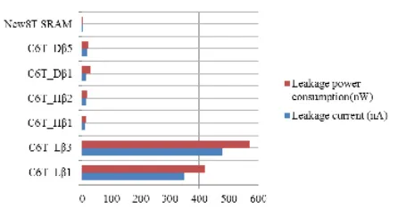
Leakage Power Consumption
In this part the evaluation of the leakage current is performed during the idle state of the memory cell. Here, asymmetrical cell structure of 6T SRAM cell shown in fig. 3(a), 3(b), and 3(c) is considered. HVT is used for high threshold voltage, LVT is for low threshold voltage and DVT is for dual threshold voltage. Generally, HVT transistor is utilized to suppress leakage current when the circuit is in idle state. LVT is used for high performance applications. DVT is also adopted to get some variation in performance parameters 19.
In this section b is varied for the conventional 6T SRAM cell and then all performance parameters
are evaluated. Table 1 and fig.5 show the simulation results of leakage current and leakage power consumption for new 8T SRAM cell and conventional 6T SRAM cell with different threshold voltage and b ratio.
Read Access Delay and write Access Delay
Read delay of 6T SRAM cell is the maximum time interval from the 50% low to high transition of word line to the 50% high to low transition of sense amplifier output. In the proposed 8T SRAM cell there is separate word line for read operation (RwL). The read access time of 8T SRAM cell is evaluated by the maximum time interval from the 50% low to high transition of read word line RwL to the 50% high to low transition of sense amplifier output.
write delay of 6T SRAM cell and 8T SRAM cell is the longest time interval from the 50% low to high transition of word line to the 50% high to
Table 1: Simulation results of leakage power consumption
Cell Leakage Leakage
current (nA) power
consu-mption (nw)
C6T_Lb1 349.104 418.8
C6T_Lb3 476.45 571.2
C6T_Hb1 11.354 13.624
C6T_Hb2 14.074 16.88
C6T_Db1 13.784 27.568 C6T_Db5 18.916 22.699
New8T SRAM 0.671 0.805
Table 2: Simulation results of read and write access delay
Cell Read access write access
delay (pS) delay (pS)
C6T_Lb1 92.87 234.10
C6T_Lb3 54.43 115.76
C6T_Hb1 312.60 940.21
C6T_Hb2 349.3 891.10
C6T_Db1 315.08 539.8
C6T_Db5 301.96 535
New8T SRAM 38.56 114.13
Fig. 5: Leakage current and Leakage power consumption
low transition of storing node (Q or QBAR). Table 2 shows the values of read and write access delay and fig.6 shows the graph.
Read Static Noise Margin (RSNM) and Hold Static Noise Margin (HSNM)
Data stability in terms of read and hold static noise margin is evaluated and analyzed in this section. These two parameters estimate the stability of the cell during read and hold state. Data stability of the cell is highly considerable constraint during read operation and hold state of the cell at nanometers technology nodes. At advanced technology data stability reduces because of the supply voltage minimization. Stability is generally defined by the static noise margin (SNM) of the cell20. SNM is the maximum value of DC noise
voltage that is tolerable by the cell without affecting the stored data of the SRAM cell1. In this paper
the SNM is calculated using butterfly curve. SNM is calculated graphically by estimating the length of maximum possible square fitted between the
voltage transfer characteristics of the cross coupled inverters 7. In ground gated 6T SRAM cell the RSNM
and HSNM are calculated at different â ratio and by utilizing LVT, HVT and DVT transistors. The RSNM of the proposed 8T SRAM cell is estimated by keeping the RwL, wwL and CS at VDD, 0v and VDD respectively.
Hold stability is calculated when the cell is in hold state.At this state the word lines are off, so the whole cell is totally disconnected from the bit lines. Table 3 and fig. 7 represent the stability in terms of RSNM and HSNM.
write Voltage Margin
write voltage margin is the measure of write ability. The maximum noise voltage necessary to flip the stored bit of the cell, defines the write voltage margin. In this paper the write ability is measured using write trip point. It shows how difficult it is to write to the storing nodes of the cell7.
The bit-line voltage is swept from 0v to VDD, and
Fig. 6: Read and write access delay with different threshold voltages and b ratio
Table 4: Simulation results of write voltage margin
Cell write voltage margin (mv)
C6T_Lb1 600.33
C6T_Lb3 627.29
C6T_Hb1 560.59
C6T_Hb2 571.54
C6T_Db1 532.13
C6T_Db5 543.07
New8T SRAM 462.93
Table 3: Simulation results of RSNM and HSNM
Cell RSNM (mv) HSNM (mv)
C6T_Lb1 0.182 0.23
C6T_Lb3 0.436 0.215
C6T_Hb1 0.465 0.284
C6T_Hb2 0.495 0.294
C6T_Db1 0.436 0.284
C6T_Db5 0.509 0.275
the flipping voltage of the cell, when Q and QBAR flip their data is noticed. The value of bit-line voltage at the crossing point of internal storage nodes Q and QBAR represents the write trip point 16. Table
4 and fig.8 represent the write voltage margin for new 8T SRAM cell and conventional 6T SRAM cell with different threshold voltage and b ratio.
Characterization of New 8T SRAM using MTCMOS Techniques
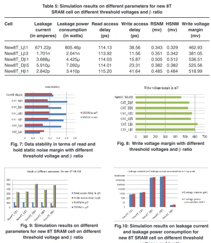
In this section the new 8T SRAM cell is examined under different b ratio and on different threshold voltages. The parameters taken for the analysis are shown in table 6 and fig. (9 and 10) depicts the pictorial analysis of different parameters.
Fig. 9: Simulation results on different parameters for new 8T SRAM cell on different
threshold voltage and b ratio
Fig.10: Simulation results on leakage current and leakage power consumption for new 8T SRAM cell on different threshold
voltages and b ratio
Fig. 7: Data stability in terms of read and hold static noise margin with different
threshold voltage and b ratio
Fig. 8: write voltage margin with different
threshold voltages and b ratio
Table 5: Simulation results on different parameters for new 8T
SRAM cell on different threshold voltages and b ratio
Cell Leakage Leakage power Read access write access RSNM HSNM write voltage
current consumption delay delay (mv) (mv) margin
(in amperes) (in watts) (ps) (ps) (mv)
It is noticed here that new 8T SRAM cell using HVT represents less leakage power dissipation as compare to other threshold voltage transistors. The LVT new 8T SRAM circuit at b=3 achieves the fastest write speed due to the low threshold transistors and using pull down transistor width 420nm. The DVT new 8T SRAM circuit with b=1 shows lowest read access delay due to low threshold voltage access transistor. DVT 8T SRAM circuit with b=1 achieves the highest RSNM, HSNM and write voltage margin.
The abbreviations used in table 5 are
New8T_Lb1: low threshold and b ratio is 1, New8T _Lb3: low threshold and b ratio is 3 New8T _Hb1: high threshold and b ratio is 1, New8T_Db1: Dual threshold and b ratio is 1, New8T_Db5: Dual threshold and b ratio is 5.
CONCLUSIONS
The new single ended 8T SRAM cell with low leakage power and high data stability
is explored in this paper. The proposed circuit consumes 805.46pw leakage power during idle state of the circuit which is very less as compare to conventional 6T SRAM cell with sleep and hold transistors. The proposed new 8T SRAM cell shows highest noise immunity 0.329mv in hold state. Furthermore, the proposed circuit represents minimum read and write access delays 114.13ps and 38.56ps respectively as compare to conventional 6T SRAM cell. Alternatively proposed single ended 8T SRAM cell with different threshold voltages and b ratio is also evaluated in section 5. That shows some further improvement is possible in terms of leakage current, data stability (RSNM and HSNM) and write voltage margin. The proposed 8T SRAM cell with HVT represents less leakage power dissipation. The LVT new 8T SRAM circuit at b=3 achieves the fastest write speed due to the low threshold transistors and pull down transistor. The DVT new 8T SRAM circuit with b=1 shows lowest read access delay. DVT 8T SRAM circuit with b=1 achieves the highest RSNM, HSNM and write voltage margin.
1. Evelyn Grossar, Michele Stucchi, karen Maex and wim Dehaene, “Read Stability and write-Ability Analysis of SRAM Cells for Nanometer Technologies” IEEE Journal of Solid state circuits, 41(11), pp. 2577-2585, November, 2006.
2. E. Seevinck, F. List, and J. Lohstroh, “Static-noise margin analysis of MOS SRAM cells”, IEEE Journal of Solid-State Circuits, SC-22, (5), pp. 748–754, October, 1987.
3. k. Roy, S. Prasad, Low Power CMOS VLSI Circuit Design, 1st edn. (wiley, New York, 2000).
4. L. Chang, R.k. Montoye, Y. Nakamura, k.A. Batson, R.J. Eickemeyer, R. H. Dennard, w. Haensch, D. Jamsek, An “8T SRAM for variability tolerance and low-voltage operation in high-performance caches”, IEEE Journal of Solid-State Circuits 43(4), 2008.
5. Ming-Hsien, J.Y. Lin, M.C. Tsai, L. Chien-Yu,
Y.J. Lin, M.H. wang, H. S. Huang, k. D. Lee, w.C. Shih, S. J. Jou, C. T. Chuang, “A single-ended disturb-free 9T subthreshold SRAM with cross-point data-aware write word-line structure, negative bit-line, and adaptive read operation timing tracing”, IEEE Journal of Solid-State Circuits 47(6), pp.1469–1482, 2012.
6. C.B. kushwah, S.k. Vishvakarma, D. Dwivedi, Single-ended sub-threshold FinFET 7T SRAM cell without boosted supply, in Proceedings of IEEE International Conference on IC Design & Technology (ICICDT), pp. 1–4, 2014.
7. Liang wen, Zhentao Li, Yong Li, “Single-ended, robust 8T SRAM cell for low-voltage operation”, Microelectronics Journal, 4(8), pp.718-728, August, 2013.
8. S. Tawfik, V. kursun, “Low power and robust 7T dual-Vt SRAM circuit”, in Proceedings of International Symposium Circuits and
Systems, pp. 1452–1455, 2008.
9. H. Jiao, V. kursun, Tri-mode operation for noise reduction and data pre servation in low-leakage multi-threshold CMOS circuits, in: J.L. Ayala, D.A.Atienza, R.Reis(Eds.),VLSI-SoC: Forward-Looking Trends in IC and Sys- tem Design, ,ISBN 978-3-642-28565-3, pp. 258–290, Springer, 2012.
10. Benton H. Calhaun, Anantha P. Chandrakasan “Static Noise Margin Variation for Sub-threshold SRAM in 65 nm CMOS”, IEEE Journal of Solid-State Circuits, 41, pp.1673-1679, July 2006.
11. Hailong Jiao, Yongmin Qiu, Volkankursun, “Variability-aware 7T SRAM circuit with low leakage high data stability sleep mode”, INTEGRATION, the VLSI journal 53, pp.68– 79, 2016.
12. H.Jiao, V.kursun, “Ground gated 8T SRAM cells with enhanced read and hold data stability”, In:Proceedings of the IEEE Computer Society Annual Symposium on VLSI, pp.52–57, 2013.
13. Liu, Z. and kursun, “Characterization of a Novel Nine-Transistor SRAM Cell”, IEEE Transactions on Very Large Scale Integration (VLSI) Systems, pp.488-492, 2008. 14. H.Jiao, V.kursun, “Asymmetrical ground
gating for low leakage and data robust sleep mode in memory banks”, In: Proceedings of the IEEE International Symposium on VLSI Design, Automation and Test, pp.205–208, 2011.
15. k.Zhang, U.Bhattachar ya, Z.Chen, F.Hamzaoglu, D.Murray, N.Vallepalli, Y.wang, B.Zheng, M.Bohr,”SRAM design on 65nm CMOS technology with dynamic sleep transistor for leakage reduction”, IEEE Journal of Solid-State Circuits 40(4) pp.895–901, 2005.
16. C. B. kushwah, S. k. Vishvakarma, D. Dwivedi, “Single-Ended Boost-Less (SE-BL) 7T Process Tolerant SRAM Design in Sub-threshold Regime for Ultra-Low-Power Applications” Springer, DOI: 10.1007/ s00034-015-0086-5, June, 2015.
17. C.B. kushwah S.k. Vishvakarma, “A sub-threshold eight transistor (8T) SRAM cell design for stability improvement”, In: Proceedings of IEEE International Conference on IC Design &Technology (ICICDT), pp. 1–4, 2014.
18. M. H. Tu, J. Y. Lin, M. C.Tsai, S. J. Jou, C. T. Chuang, “Single-ended subthreshold SRAM with asymmetrical write/read-assist”, IEEE Trans. Circuit System, I 57(12), pp. 3039–3047, 2010.
19. B.H.Calhoun, A.P.Chandrakasan, “A256-kB sub-threshold SRAM in65-nm CMOS”, in: Proceedings of International Solid-State Circuits Conference, pp. 628–629, 2006. 20. k. Takeda, Y. Hagihara, Y. Aimoto, M. Nomura,