Nonsingular Green’s Functions for Multi-Layer Homogeneous
Microstrip Lines
M. Khalaj-Amirhosseini*
Abstract: In this article, three types of green's functions are presented for a narrow strip line (not a thin wire) inside or on a homogeneous dielectric, supposing quasi-TEM dominant mode. These functions have no singularity in contrast to so far presented ones, so that they can be used easily to determine the capacitance matrix of multi-layer and single-layer homogeneous coupled microstrip lines. To obtain the green’s functions, the Laplace’s equation is solved analytically in Fourier integral or Fourier series expressions, taking into account the boundary conditions including the narrow strip. The validity and accuracy of three presented green’s functions are verified by some examples.
Keywords: Green’s Function, Singularity, Coupled Microstrip Transmission Lines.
1 Introduction1
The multiconductor coupled microstrip transmission lines are used in RF, microwave and high-speed digital circuits extensively. To analyze these transmission lines, one has to find the capacitance matrix of the structure [1]. The capacitance matrix of this structure is determined using conformal mapping transformations [2, 3], variational methods [4, 5], spectral domain techniques [6, 7], finite difference method [8], solving Laplace’s equation [9] and the combination of green’s function and method of moments [1, 10-13].
The green's functions presented in the literatures are for an infinitesimally thin wire and have singularity on the wire. In this article, some new green's functions are presented for a narrow strip line (not a thin wire) inside or on a homogeneous dielectric. These green's functions have no singularity and can be used to determine the capacitance matrix of multi-layer and single-layer homogeneous coupled microstrip lines. To obtain these green’s functions, the Laplace’s equation is solved analytically in Fourier integral or Fourier series expressions, considering the boundary conditions including the narrow strip.
In section 2, open multi-layer microstrip structure is introduced and then a closed form green’s function is obtained for open single-layer structure, in section 3. In section 4, shielded multi-layer or single-layer microstrip
Iranian Journal of Electrical & Electronic Engineering, 2013. Paper first received 3 Mar. 2013and in revised form 15 May 2013. * The Author is with the Department of Electrical Engineering, Iran University of Science and Technology, Tehran, Iran.
E-mail: [email protected].
structures are introduced and then two green’s functions are obtained for both of them. Finally, the validity of three presented green’s functions is verified by some examples, in section 5.
2 Open Multi-Layer Microstrip Structure
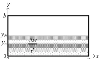
Fig. 1 shows the cross-section of a typical open and inhomogeneous N-layer microstrip line. The relative electric permittivity and top surface of layers are (n)
r ε
and yn, respectively, where n = 1, 2, …, N. There is a narrow strip of width Δw whose center is (x’,yn). It is assumed that the principal propagation mode is quasi-TEM. Now, solving the two dimensional Laplace’s equation gives the voltage distribution in the n-th region as follows.
(
)
∫
∫
∞∞ −
∞
∞ −
+ − =
=
x x x
x n x x
n
x x x
n n
dk x jk y k k B y k k
A
dk x jk y k V y
x V
) exp( ) exp( ) ( ) exp( ) ( 2
1
) exp( ) , ( ~ 2
1 ) , (
π π
( 1 )
in which V~n(kx,y) is the Fourier transform of the
voltage Vn(x,y), given by:
) exp( ) ( ) exp( ) (
) exp( ) , ( ) , ( ~
y k k
B y k k
A
dk x jk y
x V y k V
x x
n x x
n
x x n
x n
+ − =
− =
∫
∞∞
− ( 2 )
Also, the surface charge on the top side of region n is obtained like this.
Khalaj-Amirhosseini: Nonsingular Green’s Functions for Multi-Layer Homogeneous Microstrip Lines 137
∫
∞ ∞ − + + + + = + + = ⎟ ⎟ ⎟ ⎟ ⎟ ⎠ ⎞ ⎜ ⎜ ⎜ ⎜ ⎜ ⎝ ⎛ + − − − − = ⎟⎟ ⎠ ⎞ ⎜⎜ ⎝ ⎛ ∂ ∂ − ∂ ∂ = x x n x n r x n n x n r x n n x n r x n n x n r x n x y y n n r y y n n r n s dk x jk y k k B y k k A y k k B y k k A k y y x V y y x V x n n ) exp( ) exp( ) ( ) exp( ) ( ) exp( ) ( ) exp( ) ( 2 ) , ( ) , ( ) ( ) ( ) ( ) 1 ( 1 ) 1 ( 1 1 ) 1 ( ) ( 0 ) ( 0 ε ε ε ε π ε ε ε ε ρ (3)It is known that the voltage must be continuous on the interfaces between two adjacent regions. Besides, the surface charge on the interfaces between two adjacent regions is zero excepting on the strip which is assumed to be uniform. Considering these boundary conditions, the following 2N+2 equation system for 2N+2 unknown coefficients are obtained.
⎥ ⎥ ⎥ ⎥ ⎥ ⎥ ⎥ ⎥ ⎦ ⎤ ⎢ ⎢ ⎢ ⎢ ⎢ ⎢ ⎢ ⎢ ⎣ ⎡ ′ = ⎥ ⎥ ⎥ ⎥ ⎥ ⎥ ⎥ ⎥ ⎥ ⎥ ⎥ ⎥ ⎥ ⎥ ⎦ ⎤ ⎢ ⎢ ⎢ ⎢ ⎢ ⎢ ⎢ ⎢ ⎢ ⎢ ⎢ ⎢ ⎢ ⎢ ⎣ ⎡ ⎥ ⎥ ⎥ ⎥ ⎥ ⎥ ⎥ ⎥ ⎦ ⎤ ⎢ ⎢ ⎢ ⎢ ⎢ ⎢ ⎢ ⎢ ⎣ ⎡ − − − − − − − − − − − + + + + + + 0 ) , ( 0 0 ) exp( ) exp( 0 0 0 0 0 0 0 0 ) exp( ) exp( ) exp( ) exp( 0 0 0 0 ) exp( ) exp( ) exp( ) exp( 0 0 0 0 0 0 0 0 1 1 1 1 1 1 1 1 ) 1 ( ) 1 ( ) ( ) ( M M M M L L M M M M L L L L M M M M L L x k F B A B A B A B A b k b k y k y k y k y k y k y k y k y k x n N N n n n n x x n x n r n x n r n x n r n x n r n x n x n x n x ε ε ε ε (4) in which ) exp( 2 sinc ) exp( ) exp( ) , ( 1 ) , ( 0 2 / 2 / 0 0 x jk w k k dx x jk w k dx x jk y x k x k F x x x l w x w x x x l x n s x x n ′ − ⎟ ⎠ ⎞ ⎜ ⎝ ⎛ Δ = − Δ ≅ − = ′
∫
∫
Δ + ′ Δ − ′ ∞ ∞ − π ε ρ ε ρ ρ ε (5)where ρl is the per-unit-length charge of the strip. After finding the unknown coefficients An and Bn through Eq. (4), the voltage distributions are obtained using numerical calculating of the integrals in Eq. (1). Finally, the green’ function will be in fact
l n V x y
y x y x
G( , ; ′, )= ( , )/ρ .
If the electric permittivity of all layers in Fig. 1 are being the same, i.e. a homogeneous dielectric, the Fig. 1 will be reduced to Fig. 2. In fact, there will be only three regions to find potential coefficients. In view of boundary conditions, the Fourier transform of the voltages will be resulted as follows.
⎩ ⎨ ⎧ ≤ ≤ + ≤ ≤ = h y y y k B y k A y y y k A y k V n x x n x x ); cosh( ) sinh( 0 ); sinh( ) , ( ~ 2 2 1 (6) where three desired unknown coefficients are given by
(
)
(
)
(
)
(
1 coth( )coth( ))
]
) sinh( ) coth( ) tanh( 1 ) cosh( ) ( coth 1 ) ( coth ) coth( ) exp( 2 sinc 0 1 h k y k y k h k y k y k h b k h b k h k x jk w k k A x n x n x x n x n x x r x x r x x x l − − ⎢ ⎣ ⎡ − − × − + ′ − ⎟ ⎠ ⎞ ⎜ ⎝ ⎛ Δ = ε ε π ε ρ (7) ) 1 ( r
ε
) 2 ( rε
) (n rε
) (N rε
) 1 (n+ rε
1 = r ε x′Fig. 1 The cross-section of a typical open inhomogeneous multi-layer microstrip lines.
r
ε
1 = r ε rε
x′Fig. 2 The cross-section of a typical open homogeneous multi-layer microstrip lines.
⎢ ⎣ ⎡ + × − = cot 1 1 s 0 2 k A r x l ε ε ρ 0 2 k B x r l = ε ε ρ
3 Open Sin
If all the homogeneou there will be Fourier tran dielectric lay h in Eqs.
(6)-(
) ( ~ ) , ( ~0 k h h V h k V x l x = = ε ρ
---(
− + ′ − − ′ − + ⎢ ⎣ ⎡ ⎜ ⎝ ⎛ × = sgn( 2 sgn( sgn( | 1 ) , ( x x x x x x Ci h x V i π β πwhere β1 and fraction exist
0
h b
Fig. 3 The c single-layer m
(
coth ) th( coth( sinc ) inh( k h k h k y k x x r n x ε si ) sinh(kxyn xngle-Layer M
strips are situ us dielectric of
only two diff nsform of t yer will be obt -(9) as follow
(
coth( ) 2 sinc sinh( sinh( ) , ( ~ h k w k k k y k V x r x x ⎟ ⎠ ⎞ ⎜ ⎝ ⎛ Δ ε π ---Δ + ′ − ⎜⎜ ⎝ ⎛ Δ + ⎜⎜ ⎝ ⎛ Δ − ′ Δ − ′ −∫
∞ ) 2 / 2 ) 2 / 2 ) 2 / 2 / co ) , ( ~ 0 w x w w h w x h k V x π πd β2 are the m ting in Eq. (11
cross-section o microstrip lines.
(
)
⎥ ⎦ ⎤ − + ⎟ ⎠ ⎞ ⎜ ⎝ ⎛ Δ ) ( ( coth ) exp 2 c h b k b k h w k x x x π ex 2 inc kx w⎟⎠ ⎞ ⎜ ⎝ ⎛ Δ π Microstrip Str
uated on an o f height h, as ferent regions the voltage
tained by con s.
(
( coth ) exp( ) ) b k x jk y k h k x x x x − + ′ − ---− ′ − − ⎜ ⎝ ⎛ − − ⎜ ⎝ ⎛ − − ⎜ ⎝ ⎛ − ⎟ ⎠ ⎞ ≅ sgn( | | sin | ) s( x x x Si x Si x dk x k i i i x x β β βminus roots of 1), given by
y
Δw
x′
of a typical o
)
− ′ − ) ) ( h b x jkx ) xp(−jkxx′ructure
open single-la shown in Fig . In this case, distribution nsidering yn =
))
) h − (10---)
⎭ ⎬ ⎫ ⎥⎦ ⎤ Δ − ⎠ ⎞ Δ + ′ ⎠ ⎞ Δ − ′ − ⎟ ⎠ ⎞ Δ − ′ + ) 2 / | 2 / | 2 / 2 / )( 1 ( 0 w h w x h w x h w x h r l β ε πε ρ f denominator rε
1 = r ε pen homogene (8) (9) ayer g. 3, the on y =) rea (10 s ( ( ~ V × × 1.0 ≅ α Eq doi vol fol ---⎜ ⎝ ⎛ − ⎟⎟ ⎠ ⎞ ⎟ ⎠ ⎞ ⎜ ⎝ ⎛ − ⎟⎟ ⎠ ⎞ ⎟ ⎠ ⎞ ⎜ ⎝ ⎛ − − Δ −
∑
= cos cos | ) 1 2 x x x Ci w h i i i i β β β β β r of xeous Fig
After som asonable appr 0) as is seen in
ex 2 sinc | | ) 1 ( ) , ( 2 0 w k h k h h k x x r l x ⎟ ⎠ ⎞ ⎜ ⎝ ⎛ Δ + ≅ π ε ε ρ
In the fractio 0 approximate / tanh( 4 . 1 r ≅ ε
Fig. 4 show qs. (10) and (1 Substituting ing some ma ltage distribu llows. ---⎟ ⎠ ⎞ Δ + ′ ⎟ ⎠ ⎞ Δ − ′ ⎟ ⎠ ⎞ Δ + ′ ⎩ ⎨ ⎧− −
∑
= 2 / 2 / | 2 / ) 1 ( 2 1 h w x h w x h w x i i i β βg. 4 Comparing
me mathema roximation ca n the followin
) xp( /( ( | x jk b h h k x r x ′ − − + +ε
onal relation ( ed as follows
(
1.75 1.4 )3 + −
s the excellen 1) for h/(b-h)= the approxim athematical m ution on the
⎜ ⎝
⎛ − ′ −
sin i x x
i
β α
two relations 1
atical manip an be obtained ng relation. ( | | )) | h k
h x +
+
ε α α
11), α is a co
)
) 3 / tanh(
4 εr h
nt agreement =1/5 versus kx mate Eq. (11) i manipulations, surface of ⎟ ⎠ ⎞ Δ + ′ /2
h w
10 (---) and 11 (
pulations, a d for the Eq.
)) /(b h h
r+ −
ε
(11) nstant around
) /(b h
h − (12)
between two kxh.
in Eq. (1) and , leads us to dielectric as (13) (…). a . ) d o d o s
Khalaj-Amirhosseini: Nonsingular Green’s Functions for Multi-Layer Homogeneous Microstrip Lines 139
[
]
)) /( )( 1 ( 4 )) /( ( )) /( ( ) 1 ( 2 1 2 2 , 1 h b h h b h h b h r r r r r − + + − − + − + + = ε ε α ε ε ε β m (14)Also, the function sgn(.) is the signum function and the functions Ci(.) and Si(.) are the sine and cosine integrals, respectively, as follows:
∫
=x du u u x Si 0 ) sin( )
( (15)
∫
−+ +
= x du
u u x x Ci 0 1 ) cos( ) ln( )
(
γ
(16)where γ is Euler's constant equal to 0.5772… . One can sees that the green’s function (13) has no singularity at the center of narrow strip.
If the width Δw approaches zero, the voltage function will be reduced to the following relation, by equating the sinc function in Eq. (11) to 1.
{
⎪⎭ ⎪ ⎬ ⎫ ⎥ ⎦ ⎤ ⎟ ⎠ ⎞ ⎜ ⎝ ⎛ − ′ ⎟⎟ ⎠ ⎞ ⎜⎜ ⎝ ⎛ ⎟ ⎠ ⎞ ⎜ ⎝ ⎛ − ′ − − ⎢ ⎣ ⎡ ⎟ ⎠ ⎞ ⎜ ⎝ ⎛ − ′ ⎟ ⎠ ⎞ ⎜ ⎝ ⎛ − ′ × − − − + ≅∑
= + h x x h x x Si h x x h x x Ci h x V i i i i i i i r l | | sin | | 2 cos | | ) ( ) 1 ( ) )( 1 ( ) , ( 2 1 1 1 2 0β
β
π
β
β
α
β
β
β
ε
πε
ρ
(17)4 Shielded Microstrip Structures
In numerous applications, the microstrip lines are fully shielded by two lateral walls at x = 0 and x = a, as shown in Figs. 5-7. The green’s function of shielded structures can be readily obtained by considering images of the strip with respect to the left and right walls as seen in Table 1.
For shielded homogeneous multi-layer microstrips, i.e. Fig. 6, also there can be found the voltage distribution by Fourier series expansion and well-known boundary conditions (four walls and voltage and surface charge on y = yn). In view of boundary conditions and performing some mathematical efforts like as Eqs. (4) and (5), the voltage distribution will result in as follows.
⎪ ⎪ ⎩ ⎪⎪ ⎨ ⎧ ≤ ≤ ⎟ ⎠ ⎞ ⎜ ⎝ ⎛ ⎥ ⎦ ⎤ ⎢ ⎣ ⎡ ⎟ ⎠ ⎞ ⎜ ⎝ ⎛ + ⎟ ⎠ ⎞ ⎜ ⎝ ⎛ ≤ ≤ ⎟ ⎠ ⎞ ⎜ ⎝ ⎛ ⎟ ⎠ ⎞ ⎜ ⎝ ⎛ =
∑
∑
∞ = ∞ = h y y a x m a y m c a y m b y y a x m a y m a y x V n m m m n m m ; sin cosh sinh 0 ; sin sinh ) , ( 1 1 π π π π π (18)where three desired unknown coefficients are given by:
⎥ ⎦ ⎤ ⎟⎟ ⎠ ⎞ ⎜⎜ ⎝ ⎛ ⎟ ⎠ ⎞ ⎜ ⎝ ⎛ ⎟ ⎠ ⎞ ⎜ ⎝ ⎛ − − ⎟⎟ ⎠ ⎞ ⎜⎜ ⎝ ⎛ ⎟ ⎠ ⎞ ⎜ ⎝ ⎛ ⎟ ⎠ ⎞ ⎜ ⎝ ⎛ − × ⎢ ⎣ ⎡ ⎟ ⎠ ⎞ ⎜ ⎝ ⎛ ⎟ ⎠ ⎞ ⎜ ⎝ ⎛ − × ⎟⎟ ⎠ ⎞ ⎜⎜ ⎝ ⎛ ⎟ ⎠ ⎞ ⎜ ⎝ ⎛ − + ⎟ ⎠ ⎞ ⎜ ⎝ ⎛ ⎟ ⎠ ⎞ ⎜ ⎝ ⎛ ′ ⎟ ⎠ ⎞ ⎜ ⎝ ⎛ ⎟ ⎠ ⎞ ⎜ ⎝ ⎛ Δ = a h m a y m a h m a y m a y m a h b m a h b m a h m m a x m a y m a w m a n n n r r n l m
π
π
π
π
π
π
ε
π
π
ε
π
π
π
ε
ρ
coth coth 1 coth tanh 1 coth ) ( coth 1 ) ( coth coth sin sinh 2 sinc 2 0 (19) ⎥ ⎦ ⎤ ⎢ ⎣ ⎡ ⎟ ⎠ ⎞ ⎜ ⎝ ⎛ − ⎟ ⎠ ⎞ ⎜ ⎝ ⎛ + × ⎟⎟ ⎠ ⎞ ⎜⎜ ⎝ ⎛ ⎟ ⎠ ⎞ ⎜ ⎝ ⎛ − + ⎟ ⎠ ⎞ ⎜ ⎝ ⎛ ⎟ ⎠ ⎞ ⎜ ⎝ ⎛ ′ ⎟ ⎠ ⎞ ⎜ ⎝ ⎛ ⎟ ⎠ ⎞ ⎜ ⎝ ⎛ Δ − = a h b m a h m a h b m a h m m a x m a y m a w m b r r n l m ) ( coth coth 1 1 ) ( coth coth sin sinh 2 sinc 2 0π
π
ε
π
π
ε
π
π
π
ε
ρ
(20) ⎟ ⎠ ⎞ ⎜ ⎝ ⎛ ′ ⎟ ⎠ ⎞ ⎜ ⎝ ⎛ ⎟ ⎠ ⎞ ⎜ ⎝ ⎛ Δ = a x m a y m a w m m c n r lm
ε
ε
π
π
π
ρ
sin sinh 2 sinc 2 0 (21) The voltage distribution of shielded homogeneous single-layer microstrips, i.e. Fig. 7, can be found from Eqs. (18) and (19) assuming y = yn = h as the following relation.∑
∞ = ⎟ ⎠ ⎞ ⎜ ⎝ ⎛ ⎟⎟ ⎠ ⎞ ⎜⎜ ⎝ ⎛ ⎟ ⎠ ⎞ ⎜ ⎝ ⎛ − + ⎟ ⎠ ⎞ ⎜ ⎝ ⎛ ⎟ ⎠ ⎞ ⎜ ⎝ ⎛ ′ ⎟ ⎠ ⎞ ⎜ ⎝ ⎛ Δ × = 1 0 sin ) ( coth coth sin 2 sinc 2 ) , ( n r l a x m a h b m a h m m a x m a w m h x V π π π ε π π ε ρ (22)One can sees that the green’s functions (18) and (22) have no singularity at the center of narrow strip. Of course, the summations in Eqs. (18) and (22) can be truncated to M terms so as the last term is being very smaller than the first term. This gives us the following condition for Eq. (22).
Table 1The location and sign of images of the shielded strip with respect to the left and right walls.
… −4a−x′ 4a+x′ −2a−x′ −2a+x′ −x′ x′ 2a−x′ 2a+x′ 4a−x′ 4a+x′ …
−+ − + − + − + − + − + −+
x
′
Fig. 5 The cross-section of a typical shielded inhomogeneous multi-layer microstrip lines.
x
′
εrr ε
1
=
r
ε
Fig. 6 The cross-section of a typical shielded homogeneous multi-layer microstrip lines.
r ε
1
=
r
ε
x
′
Fig. 7 The cross-section of a typical shielded homogeneous single-layer microstrip lines.
⎟ ⎠ ⎞ ⎜ ⎝ ⎛ ⎟ ⎠ ⎞ ⎜ ⎝
⎛ ′
⎟ ⎠ ⎞ ⎜ ⎝ ⎛ Δ +
⎟ ⎠ ⎞ ⎜
⎝
⎛ −
+ ⎟ ⎠ ⎞ ⎜ ⎝ ⎛ >>
a x a
x a
w
h b a h
a M
r r
π π
π ε
π π
ε
sin sin
2 sin ) 1 (
) ( coth coth
(23)
5 Examples and Results
In this section we investigate the validity of three presented green’s functions (13), (18) and (22) by some examples. To get self and mutual capacitances, the lines are subdivided to K equi-potential parts of one volt potential and then the Method of Moment is used.
As a first example, consider an open single-layer microstrip transmission line of width and thickness w and h, respectively. Table 2 compares the characteristic impedance Z0 of the line obtained through Eq. (13) considering b/h=51 and K=12 with that of obtained in the references. The characteristic impedance can be obtained the following relation.
C C c Z
1 0
1
= (24)
where c is the velocity of the light and C and C1 are the capacitance of the microstrip line with and without substrate, respectively.
For the second example, consider two identical coupled lines of width w and gap s on an open single-layer dielectric of εr= 1 and b=2h. Table 3 compares the even and odd mode capacitances of the lines obtained through Eq. (13) considering K=20 with that of obtained in the reference [9].
For the third example, consider two identical coupled lines of width w lying at points (x1=6.5, y1=1) and (x2=11.5, y2=0.5) in a shielded homogeneous structure of εr= 1, a = 18 and b=5. Table 4 compares the even and odd mode capacitances of this two-layer structure obtained through Eq. (18) considering K=10 and M=300 with that of obtained in the reference [13].
For the forth example, consider eight identical coupled lines of width w = 1/16h and gap s = 1/16h on the middle of a shielded single-layer structure of εr= 12.9, a = 175/16h and b = 7.25h. Table 5 compares the 20 different coefficients of the capacitance matrix of the lines obtained through Eq. (22) considering K=20 and M=8780 with that of obtained in the reference [9].
One sees from tables 2-5 that there is an excellent agreement between the results obtained from explicit form green’s functions expressed by Eqs. (13, 18) and (22) with those reported in reliable references. Therefore one can conclude the validity of these three presented relations.
Table 2 An open single-layer microstrip transmission line (Example 1).
w/h εr C [pF/m]
Eq. (13)
C1 [pF/m]
Eq. (13)
Z0 [Ω]
Eq. (13)
Z0 [Ω]
(Refs.) 0.4 6 71.18 18.40 91.68 91.17 [13] 0.4 9.5 110.30 18.40 73.99 73.70 [13] 1 6 108.01 25.90 63.03 62.71 [13] 1.025 8.875 159.54 26.31 51.45 50.00 [8]
3 10 356.22 45.97 26.05 25.47 [12] 10 6 579.87 108.40 13.30 13.34 [13] 10 9.5 912.91 108.40 10.60 10.57 [13]
Table 3 An open single-layer microstrip coupled transmission lines (Example 2).
w/h s/h Ceven
[pF/m] Eq. (13)
Ceven
[pF/m] [9]
Codd
[pF/m] Eq. (13)
Codd
[pF/m] [9] 0.1 0.1 9.48 9.59 26.38 27.74 0.1 1 12.75 12.95 15.08 15.56
1 0.1 26.58 26.33 51.68 54.58 1 1 31.01 31.09 35.86 35.73
Table 4 A shielded two-layer microstrip coupled transmission lines (Example 3).
Eq. (18) [13]
C11 [pF/m] 49.33 49.51
C22 [pF/m] 77.08 77.12
C21 [pF/m] -1.826 -1.835
Khalaj-Amir
Table 5 A shie
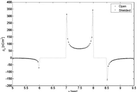
It is note of the open when the dis large relative the green’s structures an charge on th The structure on a dielectri x = 5.5, 7.5 and 0 volt, re = 11 and the One can se structures ar third strips h walls.
Fig. 8 The sur open and shiel
6. Conclusio
Three typ narrow strip homogeneou function for two series fo and single-la introduced. have a high a presented g examples. Al of open and each other at
hosseini: Non
elded single-lay
Eq. (22 [9] Eq. (22
[9]
worthy that th and shielded tance between e to height of
functions of nd vice versa he dielectric o es have three ic of εr= 5 and
and 9 and ar espectively. T e width of the ee that the re almost the have a distanc
rface charge on lded structures.
ons
pes of green's p line (not a us dielectric.
open single-l orm green’s f ayer homogen These functio accuracy. The green’s funct lso, it was sho shielded struc t some simple
nsingular Gree
yer microstrip c
C11 C1
2) 126.64 -57. 127.77 -58.
C24 C2
2) -10.42 -4.3 -10.45 -4.3
he values of g d structures ar n the strip and strip. In this c shielded stru a. Fig. 8 sho of two single-identical strip d h = 1. The s re connected t The height of t shielded struc
charge distr same, where ce of only 5h
n the dielectric o
s functions are a thin wire) One closed layer microstr functions for neous microstr ons have no e validity and a
ions are ve own that the g ctures may be
conditions.
en’s Function
coupled transm
12 C13 C
.60 -12.98 -5. .45 -13.02 -5.
25 C26 C
348 -2.315 -1. 349 -2.312 -1.
green’s functi re close toget d lateral walls case, one can uctures for o ows the surf -layer structu ps of width w strips lie at po to potentials 0 the structures
cture is a = 14 ribution of t eas the first
from two lat
of two single-la
e presented fo inside or on d form gree rip structure
both multi-la rip structures singularity accuracy of th rified by so green’s functi e used in place
ns for Multi-La
ission lines in [
C14 C15
.711 3.108 .720 3.108
-C27 C33
.445 154.83 .440 156.55
-ions ther are use pen face ures. = 1 ints 0, 1 is b 4.5. two and eral
ayer
or a n a en’s
and ayer are and hree ome ions e of
Re
[1]
[2]
[3]
[4]
[5]
[6]
[7]
[8]
[9]
[10
[11
ayer Homogen
[pF/m] (Examp
C16 C17
1.895 -1.286 1.892 -1.280
C34 C35
51.15 -10.14 51.95 -10.17
eferences
Paul C. transmissi 1994. Wheeler H parallel w approxima Tech., Vo Wan C., “ quasi-stati lines”, IE Vol. 44, N Yamashita for the an Microwav 256, Apr. Duncan J multicond Trans. Mi pp. 107-1 Itoh T. an dispersion lines”, IE Vol. 22, N Sawicki A bound c multicond using th variationa Theory Te 1986. Stinehelfe uniform Trans. Ele 506, Jul. 1 Homentco determine open mu Trans. Mi pp. 18-24, 0] Bryant T
microstrip of micros Theory Te Dec. 1968 1] Weeks W capacitanc in the pr
neous Microst
le 4).
C18 C22
-1.218 153.52 -1.211 155.23
C36 C44
-4.212 155.06 -4.213 156.78
R., Analy ion lines, Jo H. A., “Trans wide strips b ation”, IEEE
l. 12,No. 3, pp “Analitically ic parameter EEE Trans. M No. 1, pp. 75-7
a E. and Mitt nalysis of micr
ve Theory Tec 1968. J. W., “Cha ductor strip t icrowave The 18, Jan. 1965. nd Mittra R., “
n characteristi EEE Trans. M No. 10, pp. 89
A. and Sachs calculation o ductor printed he spectral– al method”, ech., Vol. 34, er H. E., “A microstrip tr ectron Device 1968.
ovschi D. and ed quasi-static ulticonductor
icrowave The , Jan. 1998. . G. and We p transmission strip lines”, Tech., Vol. 16
8.
W. T., “Calcu ce of multico esence o a d
trip Lines
C23
2 -51.71 3 -52.52
C45
6 -51.05 8 -51.86
lysis of m hn Wiley an
smission line by a conform
Trans. Micro p. 280-289, M and accuratel rs of couple Microwave T 79, Jan. 1996. tra R., “Variat rostrip lines”, ch., Vol. 16, N aracteristic im
transmission eory Tech., Vo
.
“A technique f ics of shielde Microwave T
6-898, Oct. 19 se K., “Lowe on the cap d transmissio –domain ap
IEEE Trans , No. 2, pp. 2
An accurate c ransmission es, Vol. 15, N
d Oprea R., c parameters o microstrip l eory Tech., Vo eiss J. A., “P n lines and of
IEEE Trans 6, No. 12, pp
ulation of co onductor trans
dielectric inte
141 multiconductor nd Sons Inc.,
properties of mal mapping owave Theory May 1964.
ly determined ed microstrip Theory Tech., tional method , IEEE Trans. No. 4, pp.
251-mpedances of lines”, IEEE ol. 13, No. 1,
for computing ed microstrip Theory Tech.,
974.
er and upper pacitance of on lines and pproach and . Microwave 236-244, Feb.
calculation of lines”, IEEE o. 7, pp.
501-“Analytically of shielded or lines”, IEEE ol. 46, No. 1,
Parameters of coupled pairs s. Microwave p. 1021-1027,
oefficients of smission lines erface”, IEEE r
,
f g y d p ,
d
-f E ,
g p ,
r f d d e .
f E
-y r E ,
f s e ,
f s E
Trans. Microwave Theory Tech., Vol. 18, No. 1, pp. 35-43, Jan. 1970.
[12] Postoyalko V., “Green's function treatment of edge singularities in the Quassi-TEM analysis of microstrip”, IEEE Trans. Microwave Theory Tech., Vol. 34, No. 11, pp. 1092-1095, Nov. 1986.
[13] Wei C., Harrington R. F., Mautz J. R. and Sarkar T. K., “Multiconductor Transmission Lines in Multilayered Dielectric Media”, IEEE Trans. Microwave Theory Tech., Vol. 32, No. 4, pp. 439-450, Apr. 1984.
Mohammad Khalaj-Amirhosseini was born in Tehran, Iran in 1969. He received his B.Sc., M.Sc. and Ph.D. degrees from Iran University of Science and Technology (IUST) in 1992, 1994 and 1998 respectively, all in Electrical Engineering. He is currently a Professor at College of Electrical Engineering of IUST. His scientific fields of interest are electromagnetic direct and inverse problems including microwaves, antennas and electromagnetic compatibility.