http://www.sciencepublishinggroup.com/j/ajmsp doi: 10.11648/j.ajmsp.20190402.14
ISSN: 2575-2154 (Print); ISSN: 2575-1530 (Online)
Analysis of Optical Properties of SiO
2
Thin Films for Various
Thicknesses and Substrate Material Using Matlab Code
Zina Abd Alameer Al Shadidi
1, *, Ahmad Kadhum Falih
21Department of Physics Faculty of Education/Sabr, Aden University, Aden, Yemen 2
Department of Physics Faculty of Education, Aden University, Aden, Yemen
Email address:
*
Corresponding author
To cite this article:
Zina Abd Alameer Al Shadidi, Ahmad Kadhum Falih. Analysis of Optical Properties of SiO2 Thin Films for Various Thicknesses and Substrate Material Using Matlab Code. American Journal of Materials Synthesis and Processing. Vol. 4, No. 2, 2019, pp. 75-80. doi: 10.11648/j.ajmsp.20190402.14
Received: October 23, 2019; Accepted: November 19, 2019; Published: November 25, 2019
Abstract:
Theoretical study using mathematical analysis supported by Matlab code was created, for Silicon dioxide (SiO2)thin films on various substrate materials (Aluminium, quartz, and silicon), and different thicknesses. Reflectance and transmittance of the (SiO2) thin film is strongly dependent on the electromagnetic wavelength. Many physical results were
obtained. The results obtained serve as an illustration of the feasibility of simple techniques in measuring precisely the reflectance and absorptance of the (SiO2) thin film with an error not exceeding 0.1%. The reflectance and absorptance
characteristics of multilayer thin film are strongly dependent on the wavelength of the electromagnetic waves. The effects of various substrate materials on the reflectance characteristics have been investigated by evaluating the reflectance curves of SiO2 thin films with thickness in the range of (100-1000) nm. The amplitude and periodicity of reflectance and absorptance
changed with wavelength. Also the periodicity of this variety change with the film thickness and with the substrate material. In multilayer thin-film devices, the amount of light reflected at each interface can be adjusted by adjusting many factors like film thickness and substrate materials. beams phase can be adjusted by changing the layer thickness. There are thus two parameters associated with each layer, thickness and refractive index difference between film and substrate materials, which can be chosen to give the required performance.
Keywords:
SiO2, Optical Properties, Thin Film, Matlab Code1. Introduction
Silicon oxide ( ) Thin films are the most extensively studied among different deposited materials. Because of their technological importance as dielectric protective layers in semiconductor layers, integrated circuits, waveguides, and many other applications. However, high-quality films are required for these applications. has many interesting properties that make it suitable for thin film applications [1]. SiO2 thin films have wide applications in the biomaterial
industry [2-4]. And in the electronics industry, ( ) films have an important use as the gate oxide in the semiconductor and electronic devices [5], another important use in protective layers of magnetic or optical disks and in coatings of displays [6].
Many important pieces of information required in
manufacturing optical devices, like thickness, refractive index, and wavelength dependencies of optical constants [7-9].
confinement effects and optical properties for ( ) are still computationally challenging.
In this study, a simulation of transfer matrix equations was used to study the transmission and reflectance as a function of wavelength. The reflectance-transmittance characteristics of optical thin-film have been analyzed, visualized and compared for these three different substrates. The optical transmission and reflectance spectra for a range of samples of ( ) thin films (of different thickness) were obtained by a Matlab code.
2. Theoretical Analysis and Simulation
In order to exam the optical properties of a thin film, a mathematical Matlab code was built to exam the films with a thickness range from 50 − 1000 , using a wavelength in the range 200 − 1000 from near IR- visible –near UV.
The process of designing a thin film can be done on a scientific basis before an experience, paving the way for starting the manufacture of samples on the basis of knowledge.
The complex reflection coefficient is defined as the amplitude ratio of the reflected electric field to incident electric fields. The reflectance and the phase shift between the reflected and incident waves were determined. For an incident wave function given by the following equation:
, = exp − (1)
Where represents the angular frequency of the wave traveling distance represented by r in time t through the air with wavenumber .
For a thin film surface lying in the (x-y) plane, the normal incident wave will be along (z-axis) therefore “(1)” will be:
, = exp − (2) The interface between the substrate and the thin film materials is at = !. This boundary condition implies that the transmitted wave ( ") will be at ≥ ! and the reflected wave ( $) at ≤ !.
" , = "exp " − " (3)
$ , = $exp $ − $ (4)
exp − + $exp $ − $ =
"exp " − " (5)
At = !:
exp − ! + $exp $ − $! =
"exp " − "! (6)
For = " = $
Assuming that the reflected wave has the opposite direction of the transmitted and incident waves:
= − $, "='('()* (7)
exp − +! + $exp +! = "exp , -−'('()* !./ (8)
Differentiate equation (4) with respect to z.
At ≤ ! = +, = − $
≥ ! " ='('()* (9)
− 1 exp+ − +! + 1+ $exp + +! =
− 1+'('()* "exp , - −'('()* +!./ (10)
exp − +! − $exp +! =
'()
'(* "exp ,-−
'()
'(* +!./ (11)
Adding (8), (11)
,1 +'()
'2*/ "= 2 exp [− +! -1 −
'2)
'24. (12)
" ='(4'5'(24) exp [ +! -'('()4− 1.] (13)
Subtracting (11) from (8)
$=''(27'(445'()) exp [−2 +!] (14)
Taking the refractive index representation from the following equation [11, 12]:
2 + +=:84)89*); →→ += '48:)498)*; (15)
From “(13)” & “(15)”
" ='(4'5'(24) exp [ '84:)498)*;! -'('()4− 1.] (16)
$=''(27'(445'()) exp [−2 '84:)498)*; !] (17)
Where = is the dielectric constant, > is the magnetic permeability, ? is the electric conductivity.
Reflectance =GHIJHKLHM H'HGNO L+LPJ H'HGNO (18)
Q =RS
RT= UV42
VW4XVW)RTYZ[,\UV4_4]*`])^) a-VW)VW47b./
RT (19)
Q = '24
'(45'()exp [
8)9)
'4:48*;!
-'()
'(4− 1.] (20)
Transmittance =LGP'hi\LHM H'HGNOL+LPJ H'HGNO (21)
j =Rk
RT= V42 lVW)
VW4XVW)RTYZ[,7 \UV4_4]*`])^) a/
RT (22)
T=''(27'(4 )
45'()exp [−2
8)9)
'4:48*; !] (23)
The above expressions give the reflectance and transmittance amplitude for the normal incident, in terms of refractive indices, = the dielectric constant, > the magnetic permeability, and ? the electric conductivity.
Figure 1. Represents the incident, reflected, and transmitted electrical field portion from the electromagnetic wave.
For an isotropic and homogenous thin film, a part of the incident beam will reflect at the interface and the transmitted beam will reflect again at the second interface. The matrix describes its optical characteristics calculated from the following expression [11-13]:
op q = rs tuvwb v wbyxtb
xbv wb tuvwb
z{ o b
pbq (24)
Where xh is the admittance of the subsrate medium. This expression relates to the first boundary to the field components at the next boundary. The matrix elements represent the boundary encountered by the wave as it passes through the system (1):
op q |o b
pbq (25) Where
| }∏ • tuvwa v wa yxa
xav wa tuvwa €
'
a•b ‚ (26)
The above expression for matrix M represents the characteristic matrix for the multilayer system. Where this research subjected to a one layer Sio2 thin film. Therefore the
matrix M has written in a new formula and as a 2×2 matrix:
| , bbb b / (27)
The optical admittance of the layer
xa ƒ=> a
where = & > represents the permittivity and permeability of free space respectively. Because of the dependence of the refractive index a on the polarization of the incident beam, the optical admittance equation modified as follows:
xa acos m for S-polarization
And
xa a/cos m for P_ polarization (28)
The phase shift of wave in thickness Ša is given by:
wa ‹ Œ'Ž•M•tuvma (29)
Where Ša represents the thin film layer thickness [1, 3]. The transmittance (t) and reflectance (r) coefficient calculation calculated as follows [11]:
•*
•*i))5•*••i)U5iU)5••iUU (30) •*i))5•*••i)U5iU)7••iUU
•*i))5•*••i)U5iU)5••iUU (31)
In the above matrix, the elements b ‘ Š b are imaginary, while bb ‘ Š are real. Thus the reflectance coefficient is imaginary, so the reflectance will be:
Q ∗ | | (32) T=| | (33)
Regarding that
Q & j & ” 1 (34) In the optical metrology of thin-film coatings, characterization techniques were based on least-squares fitting. The measured reflectance or transmittance spectra are widely used. The spectral characteristics usually consist of normal-incidence transmittance measurement results, where m 0.
3. Results and Discussion
3.1. Reflectance and Absorptance of (SiO2) on Different
Substrate
Figure 2 presents light reflectance as a function of the
wavelength of 700nm thickness of the film,
deposited on a differentsubstrate.
The figure shows the effects of substrate materials on the reflectance properties which have been estimated. The interference reflectance pattern due to the thin film is plainly evident over the entire wavelength range scanned, with the fringe spacing increasing with wavelength. This is in a good agreement with sultan [14], and Niizeki [15]. The difference in amplitudes is due to the different contrasts in the refractive index between the substrate and the layer.
The comparison that the amplitude and periodicity of the reflectance and are strongly affected by substrates. As seen from the figure, the reflectance of films on ”• substrate is rather high and varies between 95% and
80% . While the reflectance on quartz is the minimum and it is within 5% .
The figure illustrates that the oscillation period is also a function of substrate materials. Minimum reflectance has been obtained at some wavelengths in thin films coating on the substrate of quartz, so that it can be used as a good anti-reflector film.
in reflectance for films coating on the silicon substrate, where it decreases from 75% to 32%, while such considerable drop has not seen in other substrates. Which means that the effects of substrate on the reflectance characteristics are significantly different in various substrate materials.
Figure 2. Represents light reflectance as a function of the wavelength of 700nm thickness of ˜ • , deposited on a differentsubstrate.
The effects of substrate materials on the absorptance properties have been examined by comparing the spectrum of absorptance for different substrate materials, as shown in figure 3. The figure shows that the / films have higher absorption intensity than the other films in the whole light range. In the case of Si and quartz substrate, the absorption is observed to be increased after wavelength 300 nm, while with the ”• substrate, the absorptance is nearly constant. In the short wavelength region, the absorption enhances because of the anti-reflective effect at a continuous refractive index gradient between air and the silicon [16]. While the enhancement in absorption at high wavelength region is due to the effect of diffraction with the incident light beam. Low absorbance appears in the ultraviolet region for all samples. and, absorbance in the infrared region is significantly high for all samples.
Figure 3. Represents the effects of substrate materials on the absorptance.
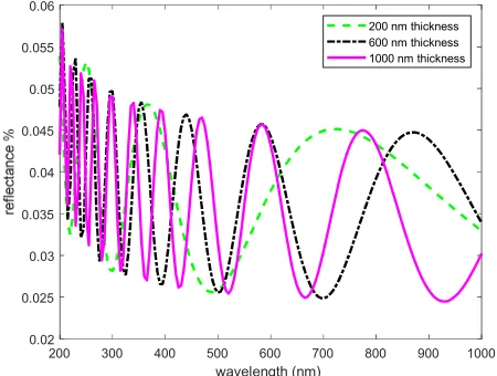
3.2. Reflectance of Multi-thickness (SiO2) on (Al) Substrate
Figure 4 shows the reflectance of with different thickness on ”• substrate. Figure 4 informs that the reflectance of light of 600 thickness was less than 82% from 680 nm to 780 nm and a minimum reflectivity at 720 nm which was 81%. Notice that the reflectance spectrum between 200 − 600 is very closed for the three thicknesses, then drops irregularly, this result have good agreement with chao wang 2017 [17].
Figure 4. shows the reflectance of with different thickness on ”• substrate.
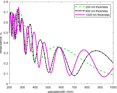
3.3. Reflectance of Multi-thickness (SiO2) on Quartz
Substrate
Figure 5 shows the reflectance spectra of the thin film coating on a quartz substrate. Although high thickness antireflection coatings can reduce reflectivity over a wide range of visible light, coatings tend to have high reflectivity at near-infrared wavelengths. From the figure, it can be seen the deviation of reflectance at a wavelength corresponding to half-wave optical thickness from the substrate reflectance. This deviation is proportional to the index variation along with the thickness.
Figure 5. Shows the reflectance spectra of the thin-film with quartz substrate.
re
fl
e
c
ta
n
c
e
%
A
b
so
rp
ta
n
ce
%
200 300 400 500 600 700 800 900 1000
wavelength (nm)
0.8 0.82 0.84 0.86 0.88 0.9 0.92 0.94
re
fl
e
c
ta
n
c
e
%
200 nm thickness 600 nm thickness 1000 nm thickness
200 300 400 500 600 700 800 900 1000
wavelength (nm) 0.02
0.025 0.03 0.035 0.04 0.045 0.05 0.055 0.06
The phenomenon of wave constructive and destructive interference can clearly explain the observed behaviors. The phenomenon of both constructive and destructive interferences is continued with higher intensity in the ranges of 500 − 1000 . The reflectance spectrum at this range shows oscillations which mean that constructive and destructive interferences occur almost at each wavelength.
3.4. Reflectance of Multi-thickness (SiO2) on Silicon (Si)
Substrate
The reflectance for thin films deposited on a silicon substrate with different thicknesses shown in Figure 6. Theoretical values of the reflectance were computed according to the relations “(30, 31, 32, 33, 34)”that take into account the wavelength dependence for the refractive index of these films.
The figure shows that the minimum in reflectance is shifted to shorter wavelengths. The difference in the optical thickness and therefore, the thickness of the layer causes the shift of the wavelength at which the reflectance would be maximal. As seen from this figure, when the period number increases the spectra become sharper, narrower, and the refractivity increased, and this result is complies with the results of Barybin and shapovalov [18], and Wen-Hao Cho [19] It is obvious that the reflectance of the layer, in this case, is independent on the thickness of the
coatings at shorter wavelength. With the thickness of SiO2 in stack increasing, the reflectance changes correspondingly. In this work, the lowest reflectance was obtained while the
thickness of was 1000 .
Figure 6. Shows the reflectance for different thicknesses of thin films deposited on the silicon substrate.
4. Conclusions
The reflectance and absorptance characteristics of the thin films have been visualized and analyzed for various substrates materials, and film thickness using Matlab code. Mathematical analyses have been done to obtain the equations of reflectance, transmittance, and absorptance. The results showed that reflectance transmittance and absorptance
of any thin film is strongly dependent on the electromagnetic wavelength. Studying the reflectance and absorptance for (SiO2) thin films, (using Matlab code), for various substrate
materials and various films thickness were done.
The results obtained represent an illustration for the benefits of the simple techniques in measuring optical properties for thin films in general, and in particular for the (SiO2) thin films. The accuracy of this method was very
excited, in which the error does not exceed 0.1%. Theoretical calculations must be done before any experiments, to save money and efforts.
It is found that multiple oscillations occur on the reflectance and Absorptance curves due to interferences among multiple reflected waves. As the wavelength increases, the oscillation period of these characteristics changes. Thus the reflectance and absorptance characteristics of multilayer thin film are strongly dependent on the wavelength of the electromagnetic waves.
The effects of various substrate materials on the reflectance characteristics have been investigated by evaluating the reflectance curves of SiO2 thin films with
thickness in the range of (100-1000) nm.
The amplitude and periodicity of reflectance and absorptance changed with wavelength. Also the periodicity of this variety change with the film thickness and with the substrate material.
In multilayer thin-film devices, the amount of light reflected at each interface can be adjusted by adjusting many factors like film thickness and substrate materials. beams phase can be adjusted by changing the layer thickness. There are thus two parameters associated with each layer, thickness and refractive index difference between film and substrate materials, which can be chosen to give the required performance.
References
[1] Ismail Oymak, Pelin Karadayı, Nuriye Sarıkaya, Tolga Tavşanoğlu > IMMC 2016 | 18th International Metallurgy & Materials Congres.
[2] M. S. W. Vong, P. A. Sermon, Thin solid films, vol. 293, p. 185, (1997).
[3] W. F. Win, B. S. Chiou, App. Surf. Sci., vol. 9 6, p 115 (1997). [4] A. Morales, A. Dura n, J. Sol-GelSci. Technol., vol. 8, P 451,
(1997).
[5] Yanyan Chen and Gang Jin, Ellipsometry, Spectroscopy V 21, no. 10, pp. 26-31, 2006.
[6] A. Ranjgar, R. Norouzi, A. Zolanvari, and H. Sadeghi, Armenian Journal of Physics, vol. 6, issue 4, pp. 198-203, 2013.
[7] N. Bouchenak Khelladi, N. E. Chabane Sari. American Journal of Optics and Photonics, vol. 1, no. 1, pp. 1-5, 2013. [8] S. A. Khodier, H. M. Sidki. journal of materials science:
materials in electronics V 12, pp. 107-109, (2001).
re
fl
e
ct
a
n
ce
[9] P. hlubina, d. Ciprian, j. lunacek, m. lesnak. Appl. Phys. B, vol. 84, pp. 511–516, (2006).
[10] Bhawana Joshi, Pratiksha Saxena, Natasha Khera. Proceedings of the 10th INDIACom; INDIACom-2016; IEEE Conference ID: 37465 2016 3rd International Conference on “Computing for Sustainable Global Development”, 16th - 18th March 2016, pp. 3871-3875.
[11] Zhang X. and Stroud D, Optical and electrical properties of thin films, Physical Reviw B, vol. 52, no. 3, (1995).
[12] Mark L. Sward, Captain, USAF, Presented to the Faculty of the School of Engineering of the Air Force Institute of Technology Air University In Partial Fulfillment of the Requirements for the Degree of Master of Science in Engineering Physics, Ohaio, (1990).
[13] V A Kheraj, C J Panchal, M S Desal, and V Potbhare, pramana journal of physics, Indian Academy of Sciences, vol. 72, no. 6, pp. 1011-1022, (2009).
[14] Md. Sultan Z and Sultana N, Journal of electrical and electronic systems, vol. 4, issu3, pp. 1-4, (2015).
[15] Tomotake Niizeki, Sachiko Nagayama, Yoshio Hasegawa, Noboru Miyata, Masae Sahara, and Kazuhiro Akutsu. Substrate Dependence and Water Penetration Structure, Coatings, vol. 6, no. 64, pp. 1-11, (2016).
[16] Nor Afifah Yahaya, Noboru Yamada, Yukio Kotaki, and Tadachika Nakayama. OPTICS EXPRESS, Vol. 21, No. 5, pp 5924-5940, March 2013.
[17] Chao Wang, Li Zhao, Zihui Liang, Binghai Dong, Li Wan, and Shimin Wang, Science and Technology of Advanced Materials (Taylor & Frances Group), vol. 18, no. 1, pp. 563-573, (2017). [18] Anatoly Barybin and Victor Shapovalov, International Journal of Optics (Hindawi Publishing Corporation), vol 10, pp. 1-18 18, (2010).