University of Pennsylvania
ScholarlyCommons
Publicly Accessible Penn Dissertations
1-1-2014
GROK-FPGA: Generating Real on-Chip
Knowledge for FPGA Fine-Grain Delays Using
Timing Extraction
Benjamin Gojman
University of Pennsylvania, [email protected]
Follow this and additional works at:
http://repository.upenn.edu/edissertations
Part of the
Computer Engineering Commons
,
Computer Sciences Commons
, and the
Electrical
and Electronics Commons
Recommended Citation
Gojman, Benjamin, "GROK-FPGA: Generating Real on-Chip Knowledge for FPGA Fine-Grain Delays Using Timing Extraction" (2014).Publicly Accessible Penn Dissertations. 1287.
GROK-FPGA: Generating Real on-Chip Knowledge for FPGA
Fine-Grain Delays Using Timing Extraction
Abstract
Circuit variation is one of the biggest problems to overcome if Moore's Law is to continue. It is no longer
possible to maintain an abstraction of identical devices without huge yield losses, performance penalties, and
energy costs. Current techniques such as margining and grade binning are used to deal with this problem.
However, they tend to be conservative, offering limited solutions that will not scale as variation increases.
Conventional circuits use limited tests and statistical models to determine the margining and binning required
to counteract variation. If the limited tests fail, the whole chip is discarded. On the other hand, reconfigurable
circuits, such as FPGAs, can use more fine-grained, aggressive techniques that carefully choose which
resources to use in order to mitigate variation. Knowing which resources to use and avoid, however, requires
measurement of underlying variation.
We present Timing Extraction, a methodology that allows measurement of process variation without
expensive testers nor highly invasive techniques, rather, relying only on resources already available on
conventional FPGAs. It takes advantage of the fact that we can measure the delay of logic paths between any
two registers. Measuring enough paths, provides the information necessary to decompose the delay of each
path into individual components-essentially, forming a system of linear equations. Determining which paths
to measure requires simple graph transformation algorithms applied to a representation of the FPGA circuit.
Ultimately, this process decomposes the FPGA into individual components and identifies which paths to
measure for computing the delay of individual components.
We apply Timing Extraction to 18 commercially available Altera Cyclone III (65 nm) FPGAs. We measure
22×28 logic clusters and the interconnect within and between cluster. Timing Extraction decomposes this
region into 1,356,182 components, classified into 10 categories, requiring 2,736,556 path measurements.
With an accuracy of ±3.2 ps, our measurements reveal regional variation on the order of 50 ps, systematic
variation from 30 ps to 70 ps, and random variation in the clusters with σ=15 ps and in the interconnect with
σ=62 ps.
Degree Type
Dissertation
Degree Name
Doctor of Philosophy (PhD)
Graduate Group
Computer and Information Science
First Advisor
Andre M. DeHon
Keywords
Subject Categories
GROK-FPGA: GENERATING REAL ON-CHIP
KNOWLEDGE FOR FPGA FINE-GRAIN DELAYS
USING TIMING EXTRACTION
Benjamin Gojman
A DISSERTATION
in
Computer and Information Science
Presented to the Faculties of the University of Pennsylvania
in
Partial Fulfillment of the Requirements for the
Degree of Doctor of Philosophy
2014
Supervisor of Dissertation Graduate Group Chairperson
Andr´e DeHon Lyle Ungar
Professor of Electrical and Systems Engineering Professor of Computer and Information Science
Dissertation Committee:
Daniel E. Koditschek, Professor of Electrical and Systems Engineering
Ali Jadbabaie, Professor of Electrical and Systems Engineering
Insup Lee, Professor of Computer and Information Science
GROK-FPGA: GENERATING REAL ON-CHIP KNOWLEDGE FOR FPGA
FINE-GRAIN DELAYS USING TIMING EXTRACTION
COPYRIGHT
2014
Acknowledgements
First and foremost I have to thank my advisor, Andr´e DeHon. His support and motivation, infinite
patience and guidance made this work possible. I have been extremely fortunate to have him as
an advisor and friend. Thank you.
I also want to thank my committee members for their advice and feedback: Daniel Koditschek,
Ali Jadbabaie, Insup Lee, and Mike Hutton.
The members of the IC Lab helped shape this work through discussions and feedback. In
particular I want to thank Raphael Rubin, Nikil Mehta, Sirisha Nalmela, and Nicholas Howarth.
Sirisha was instrumental in the developments of the Verilog used for this work. Without the
work of Nick H. the experiments varying supply voltage would not have been possible. Nick M.
developed the infrastructure to run millions of measurements, however, of most value was the
insightful discussions we had developing the ideas presented here. Finally, Rafi’s support, both
technical and intellectual, was invaluable to me. Thank you all.
I want to thank my family Marcos and Karen, Mauricio, Tanya and Gabriel, and Monica
Gojman for their love and encouragement, and Dita for knowing, with a pointed finger, that this
work would come to a successful end.
Finally, I want to thank Emily Traver. Emily has been with me through this whole process,
delighting in the ups and never failing to be there when things got rough. It has been a long road,
and I am ever grateful you were with me through every step. Your boundless love and support
ABSTRACT
GROK-FPGA: GENERATING REAL ON-CHIP KNOWLEDGE FOR FPGA FINE-GRAIN
DELAYS USING TIMING EXTRACTION
Benjamin Gojman
Andr´e DeHon
Circuit variation is one of the biggest problems to overcome if Moore’s Law is to continue.
It is no longer possible to maintain an abstraction of identical devices without huge yield losses,
performance penalties, and energy costs. Current techniques such as margining and grade binning
are used to deal with this problem. However, they tend to be conservative, offering limited
solutions that will not scale as variation increases. Conventional circuits use limited tests and
statistical models to determine the margining and binning required to counteract variation. If the
limited tests fail, the whole chip is discarded. On the other hand, reconfigurable circuits, such as
FPGAs, can use more fine-grained, aggressive techniques that carefully choose which resources to
use in order to mitigate variation. Knowing which resources to use and avoid, however, requires
measurement of underlying variation.
We present Timing Extraction, a methodology that allows measurement of process variation
without expensive testers nor highly invasive techniques, rather, relying only on resources already
available on conventional FPGAs. It takes advantage of the fact that we can measure the delay of
logic paths between any two registers. Measuring enough paths, provides the information necessary
to decompose the delay of each path into individual components—essentially, forming a system
of linear equations. Determining which paths to measure requires simple graph transformation
algorithms applied to a representation of the FPGA circuit. Ultimately, this process decomposes
the FPGA into individual components and identifies which paths to measure for computing the
delay of individual components.
We apply Timing Extraction to 18 commercially available Altera Cyclone III (65 nm) FPGAs.
We measure 22×28 logic clusters and the interconnect within and between cluster. Timing
Ex-traction decomposes this region into 1,356,182 components, classified into 10 categories, requiring
2,736,556 path measurements. With an accuracy of ±3.2 ps, our measurements reveal regional
variation on the order of 50 ps, systematic variation from 30 ps to 70 ps, and random variation in
Contents
Acknowledgements iii
Abstract iv
Glossary xvi
1 Introduction 1
1.1 Thesis . . . 1
1.2 Motivation . . . 1
1.3 Timing Extraction . . . 2
1.4 Overview . . . 3
2 Background 5 2.1 Reconfigurable Circuits . . . 5
2.1.1 Ideal Model . . . 6
2.1.2 Modern FPGAs . . . 7
2.2 Transistor Properties . . . 8
2.2.1 Delay and Energy . . . 8
2.2.2 Current-Voltage Characteristics . . . 10
2.3 Variation Sources . . . 11
2.3.1 Process Variation . . . 11
2.3.1.1 Manufacturing Process . . . 12
2.3.1.2 Variation Sources and Physical Effects . . . 14
2.3.1.3 Physical Variation and Electrical Effects . . . 16
2.4 Failure Model . . . 17
2.5 Managing Variation . . . 18
2.5.1 Testing . . . 18
3 Timing Extraction 23
3.1 Path-Delay Measurement . . . 24
3.2 Logical Component Decomposition . . . 25
3.2.1 LC Nodes as Components . . . 29
3.3 Alternate Basis . . . 31
3.4 Discrete Units of Knowledge . . . 33
3.4.1 DUK Types . . . 34
3.4.2 Incremental Path Computation . . . 34
3.4.3 DUK Decomposition . . . 35
3.4.3.1 LC Node Graph Annotation . . . 35
3.4.3.2 M-DUK Extraction . . . 36
3.4.3.3 C-DUK Extraction . . . 38
3.4.4 DUK Computation . . . 39
3.4.5 DUK Accounting . . . 41
3.4.6 DUK Graph . . . 42
3.4.7 Routing on the DUK Graph . . . 42
3.5 Measurement Precision . . . 45
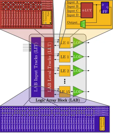
4 Timing Extraction on Commercial FPGAs 47 4.1 Cyclone Architecture . . . 47
4.1.1 LAB Architecture . . . 48
4.1.2 Interconnect Architecture . . . 49
4.2 LC Graph . . . 52
4.3 DUKs . . . 53
4.4 CAD Flow . . . 58
4.4.1 Path Measurement Circuit . . . 59
4.4.2 Control and Communication Module . . . 60
4.4.3 Path Packing . . . 62
4.4.4 Constraint Generation . . . 62
4.4.5 Bitstream Compilation and Path Measurement . . . 63
4.4.6 DUK Computation . . . 64
4.5 Experimental Setup . . . 64
4.6 Results . . . 65
4.6.3 Intra-LAB C-DUKs . . . 68
4.6.4 LAB-to-LAB C-DUKs . . . 68
4.6.5 LAB-to-General Interconnect C-DUKs . . . 71
4.6.6 Embedded Column Neighbor C-DUKs . . . 73
4.6.7 General Interconnect C-DUKs . . . 76
4.6.8 General Interconnect Sink Select C-DUKs . . . 77
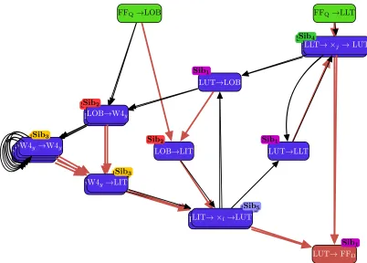
4.6.9 LLT and LIT Crosspoint Swap C-DUKs . . . 77
4.7 Falling Vs. Rising Transitions . . . 82
4.8 Intra-LUT C-DUK . . . 85
4.8.1 Results . . . 86
4.9 Effects ofVDD on Variation . . . 86
4.10 CAD Vs. Measured Delays . . . 89
4.11 Measurement Runtime . . . 91
4.12 Measurement Consistency . . . 94
4.13 Scaling . . . 96
4.14 Chapter Summary . . . 97
5 Variation Analysis 99 5.1 Variation Model . . . 100
5.2 Computingτ0and τF P GA . . . 101
5.3 Regional Variation . . . 101
5.3.1 Systematic Regional Variation . . . 103
5.3.2 Random Regional Variation . . . 105
5.4 Systematic Variation . . . 105
5.4.1 Systematic Delay Contributions . . . 110
5.5 Random Variation . . . 114
6 Future Work 116 6.1 Measurement Control and Runtime . . . 116
6.2 Beyond Logic Blocks and General Interconnect . . . 117
6.3 Beyond the Cyclone III and Cyclone IV FPGAs . . . 118
6.4 Improved Variation Analysis . . . 119
7 Conclusions 120
A Operational, Environmental, and Aging Effects 123
A.1 Operational and Environmental Variation . . . 123
A.1.1 Temperature . . . 123
A.1.2 Power Supply . . . 125
A.1.3 Crosstalk . . . 125
A.2 Aging Effects . . . 126
A.2.1 Electromigration . . . 126
A.2.2 Hot carrier injection . . . 127
A.2.3 Time-Dependant Dielectric Breakdown . . . 127
A.2.4 Negative Bias Temperature Instability . . . 128
List of Tables
4.1 Device parameters for the Cyclone III EP3C16F256C8N on the BeMicro board [8] . 48
4.2 Number of DUKs extracted from the region spanned from LAB (19,1) to LAB (40,28). 65
4.3 Average delay and frequency count breakdown over all bitstreams and measured
FPGAs . . . 93
List of Figures
2.1 Diagram of a simple FPGA showing the logic block (LB), switch box (SBox),
con-nection box (CBox), and external IO. Small circles in the SBox and CBox represent
programmable switches. . . 6
2.2 Diagram of a MOS transistor highlighting the main physical parameters,W,L, and tox. . . 8
2.3 σVth as a function of technology nodes, based on predictive technology models. Con-sidering the individual effects of random dopant fluctuations (RDF), line edge rough-ness (LER) and oxide thickrough-ness (OTF) from [99] . . . 16
2.4 Classifying a set of tested circuits into three bins, fast, medium and slow. Circuits that fail to meet a minimum threshold are thrown out. From [54]. . . 19
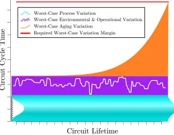
2.5 The cost of margins: Required worst-case variation margin shown as the sum of the worst-case process, environmental and operational, and aging variation. Figure not to-scale, nor meant to indicate that these three effects are completely independent . 22 3.1 Measured error rate for a path. Differentiating falling transition error rates from rising transition error rates . . . 25
3.2 Path-delay measurement circuit. . . 26
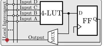
3.3 Block diagram of a 4-LUT and it’s register, along with local interconnect . . . 26
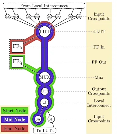
3.4 Physical resource graph of the circuit in Figure 3.3. . . 27
3.5 Transformation of a physical resource graph, where squares highlight registers and circles combinational resources, to an LC Node graph, where node names represent encompassed physical resources. Corner labels on LC Nodes, such asS1, provide convenient shorthand reference for later use in this chapter . . . 29
3.6 Path-node matrix for Figure 3.5(b) with all 11 possible paths between Start and End Nodes. . . 32
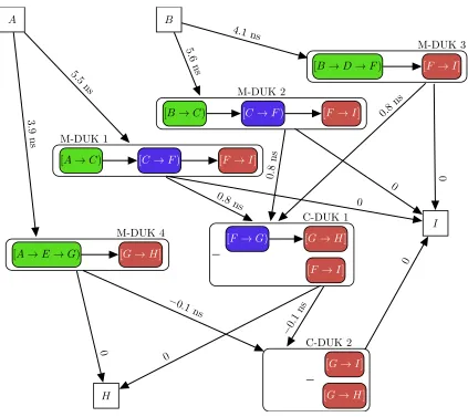
3.8 Example of the shape of DUKs . . . 34
3.9 Demonstration of how an M-DUK plus two C-DUKs leads to a path with the correct form. LC Nodes represent both a set of resources and their delay. . . 35
3.10 Result of applying Algorithm 2 to the example LC Node graph. Bold red edges show the edges marked by the algorithm . . . 37
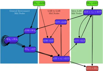
3.11 Four M-DUKs extracted from the LC Node graph in Figure 3.10 using Algorithm 4 37 3.12 Two C-DUKs extracted from the LC Node graph in Figure 3.10 using Algorithm 5 . 39 3.13 LC graph structure required to measure the delay of the M-DUK encompassing the path between nodesSA andED . . . 41
3.14 Example of the LC graph structure required to measure the delay of the C-DUK enclosed in the outline . . . 41
3.15 DUK Graph derived from the LC Node graph in Figure 3.10 . . . 43
3.16 Modified DUK Graph with register nodes, ready for running Bellman-Ford. Edges are annotated with the delay of the DUK they point to . . . 44
4.1 The BeMicro FPGA Evaluation Kit with a Cyclone III FPGA. . . 48
4.2 Cyclone III block-level floorplan. . . 49
4.3 Detailed architecture of a Cyclone III LAB. . . 50
4.4 Interconnect Architecture of a Cyclone III. Showing connections for the central, high-lighted LAB . . . 51
4.5 Connections between structures in the Cyclone III . . . 51
4.6 Physical resource graph for the Cyclone III . . . 52
4.7 LC Node graph for the Cyclone III. LC Nodes with crosspoints or wires as physi-cal resources are shown overlapped to signal all versions of that node generated by substituting the correct crosspoints or wires. . . 53
4.8 Annotated LC Node graph for the Cyclone III. Bold red edges show marked edges by Algorithm 2. Nodes belonging to a sibling set with more than one Node have tags Sibx, indicating which sibling set they belong to . . . 54
4.9 M-DUKs for the Cyclone III . . . 54
4.10 C-DUKs from sibling set 1 for the Cyclone III . . . 55
4.11 C-DUKs from sibling set 2 for the Cyclone III . . . 55
4.12 C-DUKs from sibling set 3 for the Cyclone III . . . 56
4.13 C-DUK from sibling set 4 for the Cyclone III . . . 56
4.14 C-DUK from sibling set 5 for the Cyclone III . . . 56
4.16 Block diagram of the full Timing Extraction system used to characterize delays in
the Cyclone III FPGA. . . 60
4.17 PLL resolution showing the smallest delay increment at a particular frequency. . . 61
4.18 Placement of full system on the Cyclone III for a bitstream with 5 path measurement
circuits. . . 63
4.19 Routing resources of full system on the Cyclone III for a bitstream with 5 path
measurement circuits . . . 64
4.20 Intra-LAB M-DUK structure annotated with three SDs identified by indicesi,j, andk 66
4.21 Path highlighting physical resources used by the Intra-LAB M-DUK . . . 67
4.22 Delay distributions for the Intra-LAB M-DUK. Differentiating LUT input used by
the DUK . . . 67
4.23 LAB-to-LAB M-DUK structure annotated with four SDs identified by indices i, j,
k, and l . . . 68
4.24 Path highlighting physical resources used by the LAB-to-LAB M-DUK . . . 68
4.25 Delay distributions for the LAB-to-LAB M-DUK. Differentiating LUT input used
and path direction . . . 69
4.26 Intra-LAB C-DUK Structure annotated with three SDs identified by indicesi,j, andk 69
4.27 Path highlighting physical resources used by both Tails of the Intra-LAB C-DUK . . 69
4.28 Delay distributions for the Intra-LAB C-DUK. Differentiating LUT input used by
the DUK . . . 70
4.29 LAB-to-LAB C-DUK structure annotated with four SDs identified by indicesi,j,k,
andl . . . 70
4.30 Path highlighting physical resources used by both Tails of the LAB-to-LAB C-DUK 70
4.31 Delay distributions for the LAB-to-LAB C-DUK. Differentiating LUT input used
and path direction . . . 71
4.32 LAB-to-General Interconnect C-DUK structure annotated with eight SDs identified
by indices fromito p . . . 71
4.33 Path highlighting physical resources used by both Tails of the LAB-to-General
In-terconnect C-DUK . . . 72
4.34 Delay distributions for the LAB-to-General Interconnect C-DUK. Both LUT inputs
fixed to C. Differentiating routing resource direction of the Desired Tail and
4.35 Delay distributions for the LAB-to-General Interconnect C-DUK. Fixed the Desired
Tail’s routing resource to a horizontal R4 and the Current Tail’s direction right.
Differentiating both LUT inputs used . . . 73
4.36 Embedded Column Neighbor C-DUK structure annotated with nine SDs identified
by indices fromito q . . . 74
4.37 Path highlighting physical resources used by both Tails of the Embedded Column
Neighbor C-DUK . . . 74
4.38 Delay distributions for the Embedded Column Neighbor C-DUK. Fixed routing
re-source type from C4 to C4. Differentiating both LUT inputs used . . . 75
4.39 Delay distributions for the Embedded Column Neighbor C-DUK. Fixed routing
re-source type from C4 to C4 and LUT inputs to D for the Desired Tail and C for the
Current Tail. Differentiating direction routing resource wires . . . 75
4.40 General Interconnect C-DUK structure annotated with eight SDs identified by indices
from itop . . . 76
4.41 Path highlighting physical resources used by both Tails of the General Interconnect
C-DUK . . . 76
4.42 Delay distributions for the General Interconnect C-DUK. Fixed both routing resource
type to C4. Differentiating both LUT inputs used . . . 77
4.43 Delay distributions for the General Interconnect C-DUK. Both LUT inputs fixed to
C. Differentiating routing resource type combinations . . . 78
4.44 General Interconnect Sink Select C-DUK structure annotated with seven SDs
iden-tified by indices from itoo . . . 78
4.45 Path highlighting physical resources used by both Tails of the Sink Select C-DUK . 78
4.46 Delay distributions for the General Interconnect Sink Select C-DUK. Fixed routing
resource type to C4. Differentiating both LUT inputs used . . . 79
4.47 LLT Crosspoint Swap C-DUK structure annotated with five SDs identified by indices
i, j,k,l, andm . . . 80
4.48 Path highlighting physical resources used by both Tails of the LLT Crosspoint Swap
C-DUK . . . 80
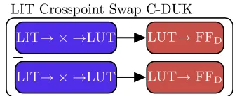
4.49 LIT Crosspoint Swap C-DUK structure annotated with five SDs identified by indices
i, j,k,l, andm . . . 80
4.50 Path highlighting physical resources used by both Tails of the LIT Crosspoint Swap
4.51 Delay distributions for the LLT Crosspoint Swap C-DUK. Differentiating both LUT
inputs used . . . 81
4.52 Delay distributions for the LIT Crosspoint Swap C-DUK. Differentiating both LUT
inputs used . . . 81
4.53 Delay distributions for the LAB-to-LAB M-DUK. Differentiating LUT input used
and path direction . . . 83
4.54 Correlation between falling and rising LAB-to-LAB M-DUK delays. Figure a shows
the result when LUT input is fixed at C and the path direction is left, while Figure b
shows the results for the same LUT input, C, but path direction is right. Diagonal
lines indicate the difference between the two results in terms ofd∆= 1.6 ps. Thicker
lines indicate 10d∆. Red dashed lines indicate error boundaries as computed in
Section 3.5. . . 84
4.55 Correlation between falling and rising LAB-to-LAB M-DUK delays. Figure a shows
the result when LUT input is fixed at D and the path direction is left, while Figure b
shows the results for the same LUT input, D, but path direction is right. Diagonal
lines indicate the difference between the two results in terms ofd∆= 1.6 ps. Thicker
lines indicate 10d∆. Red dashed lines indicate error boundaries as computed in
Section 3.5. . . 84
4.56 C-DUK for internal LUT structures . . . 85
4.57 Intra-LUT C-DUK delays. Each scatter plot shows the delay of Intra-LUT C-DUKs
with the same controlling and fixed LUT inputs. The region between red dashed lines
is shown as a reference of the range of the expected error as computed in Section 3.5 86
4.58 Architecture of the Cyclone-III 4-LUT [6] . . . 87
4.59 Intra-LAB delays when varyingVdd. DifferentiatingVdd value, Cyclone IV . . . 88
4.60 Correlation between measured DUK delays and CAD DUK delays for LAB-to-LAB
C-DUKs on LUT input C going left. Diagonal lines in Figure c, spaced at 10 ps
intervals, show the angle where perfect correlation would occur. . . 90
4.61 Correlation of CAD DUK delays to different DUK parameters. . . 90
4.62 Correlation between measured DUK delays and CAD DUK delays for LAB-to-LAB
C-DUKs on LUT input C, going left, using LUT number 7. Diagonal lines in Figure
c, spaced at 10 ps intervals, show the angle where perfect correlation would occur. . 91
4.63 Breakdown of how long each bitstream takes to run for a given FPGA. Left side
shows the breakdown for each bitstream ordered by total runtime. Right side shows
4.64 Floor plan of two bitstreams measuring the same paths, but having different
place-ment constraints. . . 94
4.65 Correlation between row-major and column-major delay measurement results. Fig-ure a shows the result when limited constraints are imposed as opposed to FigFig-ure b where placement and routing were heavily constrained. Diagonal lines indicate the difference between the two results in terms of d∆ = 1.6 ps. Thicker lines indicate 10d∆. Red dashed lines indicate error boundaries as computed in Section 3.5. . . 95
4.66 Correlation between DUKs when measuring different path sets yielding the same DUKs. Diagonal lines indicate difference between results in terms of ∆clock= 1.6 ps. Thicker lines indicate 10·∆clock. Red dashed lines indicate error boundaries as com-puted in Section 3.5. . . 96
4.67 Delay of a C-DUK from LE 6 to LE 11 in LAB (27,22) using input D, computed using 150 different pairs of paths. The distance between horizontal gray lines is ∆clock= 1.6 ps. The region between red dashed lines shows expected error bounds as computed in Section 3.5. All 150 C-DUKs are within these bounds. Cyclone III . 96 5.1 τF P GAfor LAB-to-LAB MDUKs from the 18 measured FPGAs, showing the differ-ence between falling and rising transition . . . 102
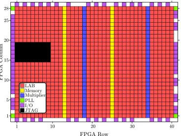
5.2 Regional Systematic Variation shown on a floor plan of the Cyclone III FPGA . . . 104
5.3 Regional Random Variation of FPGA 4RE75, shown on a floor plan of the Cyclone III FPGA . . . 106
5.4 Regional Random Variation of the LAB-to-LAB M-DUK for first 9 Measured FPGAs, shown on a floor plan of the Cyclone III FPGA . . . 107
5.5 Regional Random Variation of the LAB-to-LAB M-DUK for second 9 Measured FPGAs, shown on a floor plan of the Cyclone III FPGA . . . 108
5.6 Systematic variation internal to the LAB . . . 111
5.7 Systematic variation of LAB-to-LAB connections . . . 111
5.8 Systematic variation of general interconnect wire type . . . 112
5.9 Systematic variation of the General Interconnect . . . 113
Glossary
Timing Extraction
Child DUK (C-DUK)
The difference of two short LC Node path tails. Extends and modifies paths represented
with DUKs
Current Tail
The subtrahend of a C-DUK. Representing the tail a path must match for this C-DUK to
be applicable
Desired Tail
The minuend of a C-DUK. Representing the path tail that will remain after the C-DUK is
used
Discrete Unit of Knowledge (DUK)
Small linear combination of LC Nodes
End Node
An LC Node whose last physical resources is a register. All other physical resources are
combinational
LC Node graph
A graph representing some physical resource graph using LC Nodes
Logical Component Node (LC Node)
Group of connected physical resources that cannot be independently measured. Represents
short path from a source register node, or node with fan-in greater than one, to a sink
register node, or node with fan-in greater than one
Marked Sibling
An LC Node whose incoming edges are all annotated or marked
Mid Node
An LC Node whose physical resources are all combinational
Mother DUK (M-DUK)
A shortest path from a Start Node to an End Node. Forms the beginning of any path
represented with DUKs
Physical Resource Graph
Graph of the physical resources of a circuit
Sibling Set
A set of LC Nodes sharing the same set of LC Node parents in an LC Node graph
Start Node
An LC Node whose first physical resources is a register. All other physical resources are
combinational
Timing Extraction on Commercial FPGAs
4-LUT
4-input lookup table. Capable of implementing any 4-input boolean function
C16 bundle
In Cyclone III, group of directed vertical routing wires spanning 16 LABs
C4 bundle
In Cyclone III, group of 24 directed vertical routing wires spanning 4 LABs
Embedded Column Neighbor C-DUK
Cyclone III C-DUK interchanging the last W4 of a path with another W4. Applicable only
to paths ending at a LAB next to an embedded column
FFD
Input of a register
FFQ
General Interconnect C-DUK
Cyclone III C-DUK extending the end of a path through a W4 wire
General Interconnect Sink Select C-DUK
Cyclone III C-DUK selecting LAB sink of a W4 wire
Intra-LAB C-DUK
Cyclone III C-DUK extending the end of a path to another LE within the same LAB as the
end of the original path
Intra-LAB M-DUK
Cyclone III M-DUK representing a path between two LEs in one LAB
LAB Input Track (LIT)
Brings external signals into a LAB
LAB Local Track (LLT)
Enables direct communication between Logic Elements within one LAB
LAB Output Buffers (LOBs)
Allows signals to leave a LAB
LAB-to-General Interconnect C-DUK
Cyclone III C-DUK changing the end of a path from a horizontally adjacent LAB to a W4
wire
LAB-to-LAB C-DUK
Cyclone III C-DUK extending the end of a path to an LE in a horizontally adjacent LAB
LAB-to-LAB M-DUK
Cyclone III M-DUK representing a path from an LE in one LAB to an LE in a horizontally
adjacent LAB
LIT Crosspoint Swap C-DUK
Cyclone III C-DUK swapping LIT crosspoint used at the end of a path
LLT Crosspoint Swap C-DUK
Cyclone III C-DUK swapping LLT crosspoint used at the end of a path
Logic Array Block (LAB)
Logic Element (LE)
A small compute block, for the Cyclone III consisting of a 4-LUT and optional register
R24 bundle
In Cyclone III, group of directed horizontal routing wires spanning 24 LABs
R4 bundle
In Cyclone III, group of 34 directed horizontal routing wires spanning 4 LABs
Subspecies Difference (SD)
A minor morphological difference within a DUK type. For example, the LUT input SD
differentiates which LUT input a DUK uses
W4
group of directed routing wires spanning 4 LABs, applicable in vertical or horizontal direction
Variation Analysis
Random Regional Variation Regrand(x, y)
Regional variation unique to one FPGA
Random Variation Rand
The variation that cannot be explained by any correlated variation, quantifying the random
variation in a DUK
Regional Variation Reg(x, y)
A regional correlation function that explains how the DUK delay changes as a function of
its physical position (x, y)
Systematic Regional Variation Regsys(x, y)
Regional variation that is common to all FPGAs
Systematic Variation Sys(sd1, . . . , sdn)
A systematic correlation function composed of the product of a set of functions that correlate
delay changes to subspecies differences
τ0
A base delay for a given DUK type
τF P GA
Chapter 1
Introduction
1.1
Thesis
The resource graph of an FPGA is algorithmically decomposed into discrete units. Using only
resources within the FPGA, the delay of each of these units is computed by measuring and
linearly combining the delay of two or three paths within the FPGA. These unit delays reveal
the magnitude and composition of process variation within the FPGA, and provide the necessary
knowledge to perform component-specific mappings to mitigate adverse process variation effects.
1.2
Motivation
Circuit process variation is quickly becoming one of the biggest problems to overcome if Moore’s
Law is to continue. It is no longer possible to maintain an abstraction of identical devices without
incurring huge yield losses, performance penalties, and high energy costs. Current techniques
such as margining, where the circuits are rated to operate slow enough to capture the worst-case
transistor on a billion-transistor chip operating in worst-case conditions, and grade binning, which
classifies circuits into a limited set of performance classes, are used to deal with this problem.
However, they tend to be too conservative, only offering a limited solution that will not scale as
variation increases. Conventional circuits use statistical models and a limited number of expensive
tests to determine the margining and binning parameters needed to counteract variation. If
the limited tests give a negative prognosis, the whole chip is discarded. On the other hand,
reconfigurable circuits, such as FPGAs, can use more fine-grained and aggressive techniques that
carefully choose which resources to use in order to mitigate the adverse variation effects. These
require measurement of the underlying variation, which many considered too expensive to be
process variation due to manufacturing, without the need for expensive testers nor highly invasive
techniques, rather, relying only on resources already available on conventional FPGAs.
Modern FPGAs have billions of transistors, each with a unique set of characteristics. Some
exhibit regional variation such as differences in oxide thickness, while other effects, such as dopant
density, present themselves as stochastic variation. Beyond manufacturing process variation,
cir-cuits suffer from environmental and operational variation, such as self-heating, and aging effects.
In order to prevent these sources of variation from leading to a computational fault,
manufac-turers currently rate the performance of their circuits well below what the wires and transistors
composing them are capable of delivering. In this way, they margin against all variation sources.
Timing Extraction allows us to measure the process variation and, with that information, reclaim
the process margins added by vendors. Reducing margins leads to FPGAs with improved
per-formance and energy efficiency. Furthermore, as more and more, smaller and smaller devices are
integrated into one circuit, it is essential to fully understand the variation in the circuit if we are
to successfully utilize it and extract its full capacity, otherwise we run the future risk of variation
overwhelming circuits to the point of complete yield loss.
1.3
Timing Extraction
It is not possible to directly measure the characteristics of every transistor or wire in an FPGA.
Nevertheless, we introduce a novel technique that discovers the individual characteristics. Utilizing
only the logic available in the FPGA, we perform a careful set of tests and use the results from
those tests to discover the variation of each component.
In an FPGA, we can measure the delay of a path without the need of any extra testers by
surrounding it with two registers which are already part of the reconfigurable fabric. For
conve-nience we will label them the launch and capture registers. Starting with a low clock frequency,
we send a signal from the launch register, through the path, to the capture register. If, in the
alloted clock time we see the signal at the capture register, then we know the path is faster than
the current clock frequency. If the signal does not appear on the capture register in time, then the
path is slower. By adjusting the frequency of the clock and repeating this process it is possible to
precisely measure the path delay [93,58].
The path is composed of multiple components, our goal is to discover the variation of each
component. By configuring the correct set of overlapping paths and measuring, we can setup a
system of equations that, when solved, gives the individual delay of each component in the paths
Consider we measure three paths. Path 1 composed of component A andB. Path 2, B andC.
Finally, Path 3,C andA. Suppose the delays of the paths are 5ps, 4ps and 3ps respectively. That
leads to the system of equations below:
A+B= 5ps Path 1
B+C= 4ps Path 2
C+A= 3ps Path 3
Even though we did not measure the delays directly, with little work we can solve for the delay of
A,B, andC to be 2ps, 3ps and 1ps respectively.
Timing Extraction does exactly this but at a level that allows us to characterize a full FPGA.
Timing Extraction takes as input a directed graph representation of the resources in an FPGA.
After a series of graph transformations, it decomposes the FPGA into components formed by a
small number of resources. Based on this decomposition, it extracts and measures the delay of a
set of paths, and uses the path delays to compute the delay of each component.
Once we have the component delays, we can classify the type of variation present intoregional
variation, where variation is correlated to a physical region of the FPGA, systematic variation,
where unique properties of the component determine the variation, such as the direction of a
wire, and random variation brought about by the stochastic nature of some of the underlying
processes used during fabrication. Moreover, we can analyze and separate variation common
across FPGAs from variation unique to a particular FPGA. Quantifying how much variation
there is and what type it is allows FPGA CAD tools to produce improved logic mapping results,
including a component-specific mapping tailored to the FPGA being programmed [89, 33, 63].
Furthermore, this knowledge may be a requirement if we are to successfully use future technologies
[28]. Finally, understanding variation at this detailed level, over such a vast number of devices
can prove invaluable to circuit design in general.
1.4
Overview
The remainder of this dissertation is organized as follows. Chapter 2 presents the background
necessary for the rest of this work. It begins by giving a brief review of reconfigurable logic and
FPGAs in particular. Then, it sets up the relationship between physical properties, such as a
transistor’s length, and the electrical characteristics of wires and transistors. With this base, it
enters into a short discussion on current techniques used to manage variation.
Chapter 3, details how Timing Extraction works. It begins by developing the graph
trans-formation algorithms necessary to decompose the resource graph of an FPGA into individual
components. It then explains how to extract the set of paths necessary to compute the delay of
each component. Using the delay of the individual components, it constructs a new circuit graph
that routing algorithms can use to find shortest paths unique to that FPGA. Finally, it calculates
the expected measurement precision.
Applying Timing Extraction to an Altera Cyclone III FPGA is the subject of Chapter 4. We
first present the architecture of this FPGAs. We ground the decomposition algorithms from the
previous chapter by examining the result of applying them to this architecture. We then consider
the extra CAD steps necessary to actually measure the paths determined by the algorithm. After
explaining our experimental setup, we present the delays for the different types of measured
com-ponents. The chapter then looks at a number of results enabled by knowledge of these component
delays. It concludes by quantifying how long the measurement takes, and showing that we can
consistently measure the same component delay multiple times.
In Chapter 5 we present the techniques to separate the raw process variation into correlated
and random variation. Throughout the chapter, we apply these techniques to the results obtained
in Chapter 4, quantifying the magnitude and types of variation in the Cyclone III FPGAs.
Timing Extraction provides a complete approach to decomposing and measuring the process
variation of an FPGA; however, there is work that can improve its performance. Furthermore,
the decomposition in Chapter 5 asumes a simplifed timing model, a more precise model would
better quantify the different variation types. Chapter 6 presents future directions that address
Chapter 2
Background
Reconfigurable circuits are more amenable than other circuits to reclaiming the performance and
efficiency lost to process margins. The reason for this is that reconfigurable circuits have the
ca-pability to carefully choose which transistors and wires to use post-fabrication, once their
charac-teristics have been measured. The CAD tools can then carefully select these resources, optimizing
the circuit being mapped so that it operates well beyond the conservative operating parameters
set by the manufacturer, while still maintaining logical correctness.
Before exploring how margins are reduced and how reconfigurable circuits meet these
con-straints despite the myriad sources of variations, we must first have a firm understanding of what
modern reconfigurable circuits, such as field programmable gate arrays (FPGAs), are, what their
structure is, and how they are utilized. Furthermore, a deep understanding of the different sources
of variation will clarify future discussions. Finally, a presentation of how variation is currently
dealt with, through margining and binning, gives the required context to frame the techniques
proposed later in this thesis.
In this chapter, we present the background that will form the foundations for the rest of this
work. Readers familiar with modern FPGAs may move directly to Section 2.2.
2.1
Reconfigurable Circuits
Reconfigurable circuits provide the efficiency of hardware with the flexibility of software. They
consist of small programmable elements that perform simple logic computations, embedded in a
general routing structure. The post-fabrication flexibility that reconfigurable circuits provide is
the key feature that makes them an ideal choice for dealing with the extreme variation expected in
coming technology nodes. We focus on FPGAs, as they represent the most advanced incarnation
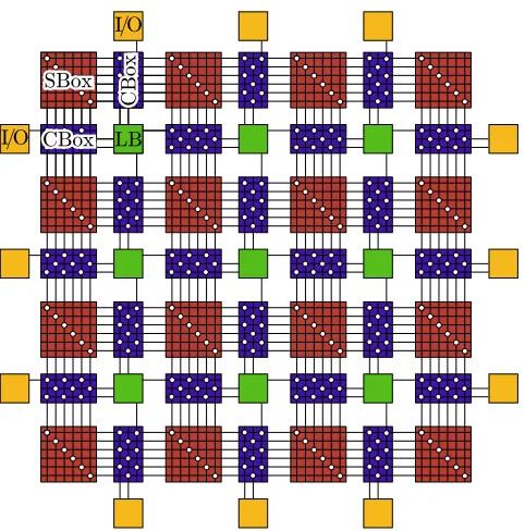
Figure 2.1: Diagram of a simple FPGA showing the logic block (LB), switch box (SBox), connec-tion box (CBox), and external IO. Small circles in the SBox and CBox represent programmable switches.
this technology (Section 2.1.1). With the basics established, Section 2.1.2 introduces the advances
applied to modern FPGAs.
2.1.1
Ideal Model
The simplest FPGA model that encompasses many of the intricacies of the technology is shown
in Figure 2.1. Along with the logic blocks(LB) familiar to all reconfigurable circuits, this FPGA
introduces a connection block and a switch block. The connection block or CBox connects the LB
to the nearest routing resources, allowing it to pick its inputs and output from an arbitrary routing
track on the interconnect network. The SBox, as the switch blocks are commonly known, appears
at the intersection of horizontal and vertical routing tracks. It consist of a set of programmable
connections that allow a signal coming in to the SBox to continue on another track in one of three
possible direction, left, forward or right. Finally, the LB is composed of a programmable 4 to 6
input gate that can be configured to compute any 4 to 6 input logic function. The output can
then, optionally be registered using a flipflop before connecting to the interconnect.
Practically, logic blocks are implemented by small memories known as lookup tables (LUTs).
The input to the LUT acts as an address to a memory cell where the result is stored. Moreover,
available, nor can a signal rout from any track in an SBox to any other routing track. This
depop-ulation of switches is beneficial because it reduces area, while still allowing for rich interconnect
that can accommodate most any routing requirement [61,73,50].
Typically, SRAM cells are used to store the programming of each switch. For a particular
computation implemented on an FPGA, the state of these SRAM cells along with the configuration
of the LUTs form what is called abitstream. The bitstream is the end result of the FPGA CAD
flow, a process that starts with a description of the computation, either in some high level language
such as C or Java [16], or some high level hardware description language such as VHDL or Verilog
[74]. Between the high level description and the bitstream the circuit description goes through a
set of transformations, including a technology mapping that modifies the logic to fit the target
device, placement, which distributes the logic over individual LBs, and routing, which figures out
how to use the interconnect to connect the LBs as required.
2.1.2
Modern FPGAs
Modern FPGAs have evolved from the simple model described above to include many advances
that improve performance, reduce energy and allow the FPGA to better capture the desired
computation.
The logic block has grown in complexity from a simple LUT-flipflop pair to what Altera calls
a Logic Array Block (LAB) [10] and Xilinx, a Complex Logic Block (CLB) [96]. Essentially,
they are groups of LUTs and registers with a small amount of local interconnect that allows for
more complex and localized computation. These structures also include dedicated carry chains to
implement adders and other logic that fits that compute pattern. Moreover, modern FPGAs are
no longer homogeneous arrays of LBs, rather they include a majority of LBs with a handful of
specialized or embedded blocks. These include multipliers, memories and even small processors
[36].
The interconnect has also matured. Instead of length one connections between SBoxes, FPGAs
now include segments of different lengths. What’s more, the interconnect is hierarchical, with
shorter segments connecting directly to LBs and longer segments connecting only to shorter
seg-ments. This structure allows signals to more efficiently traverse long distances. LBs can also
communicate directly with neighboring LBs via dedicated direct connections between LBs, giving
even more flexibility when routing signals. Finally, FPGAs have moved from bidirectional wires to
direct drive, where pairs of wires have a dedicated routing direction, one routing in one direction,
and the other in the opposite. This advancement simplifies the interconnect switches and has
Source Gate Drain
Length Oxide Thickness tox
L W
Width
Figure 2.2: Diagram of a MOS transistor highlighting the main physical parameters, W,L, and
tox.
of phase locked loops, or PLLs, that enable programmable clock frequencies. This, along with a
complex series of clock distribution networks provide Timing Extraction with the necessary tools
to measure path delays in FPGAs.
2.2
Transistor Properties
The MOS transistor is the workhorse of integrated circuits. Its miniaturization has enabled
in-novations and industries that touch almost every aspect of our lives. However, the ability to
integrate billions of transistors in one chip is not without its challenges. As we continue to push
down the dimensions of these devices, effects that previously were negligible become dominant.
With so many small transistors in the same circuit, variations between them are inevitable.
Variations lead to changes in the performance and efficiency of our circuits. In this section we
explore the physics that explain the behavior of a transistor. Figure 2.2 shows a simple diagram of
a transistor to help ground some of its parameters referenced in this section. This analysis allows
Section 2.3 to easily connect physical variations to circuit behavior.
2.2.1
Delay and Energy
Understanding how the delay and energy dissipation of a transistor relate to physical properties
such as transistor channel length, gives context as to why physical variations directly lead to
changes in circuit performance and efficiency. To start this discussion, we formally look at the
To estimate the propagation delay through a transistor, to a first order, we can model the
channel between the source and drain as a resistance, R, and consider how long it takes to
charge or discharge the capacitive load seen by the transistor,Cl, including wires and downstream
transistors, through the channel. The delay is simply
τpd=Cl·R
From Ohms law we know thatRcan be modeled as the voltage difference between the source and
drain terminals, Vds, over the current flowing through the transistor channel,Ids. Therefore, the
propagation delay of a transistor, τpd is given by
τpd =Cl· Vds
Ids (2.1)
In conventional CMOS, Vds is at most equal to the supply voltage, Vdd, but varies depending
on how the transistor is used. Ids however, varies depending on the voltages difference applied
between the gate and source terminals. We will return to how Ids behaves in the next section.
To talk about the energy per operation of a transistor it is helpful to consider the transistor as
being part of a CMOS gate with a pull-up network formed by p-type transistors and a pull-down
network implemented in n-type transistors. In this frame of reference, a transistor will either be
“on”, allowing charge to flow through its channel or “off”, trying to prevent charge from flowing.
Due to a number of effects [75,66], a transistor that is supposed to be off allows a small amount
of current to flow. We refer to this as Ids,sub and will discuss it later. Assuming that the cycle
time, determined by the frequency at which the circuit is running, is τcycle, the energyleaked by
an off transistor is expressed as
Eleak =Ids,sub·Vds·τcycle (2.2)
To contrast, a transistor that is on will allow enough current through to charge (p-type
tran-sistor) or discharge (n-type trantran-sistor) the capacitive loadCl. The energy consumed by charging
or dischargingCl through the transistor is
Eswitch=Cl·(Vds)2 (2.3)
The total energy used by a circuit in a cycle,Etotal, is then given by the sum of theEswitchof
Etotal =
X
i∈on
Eswitch(i) +
X
j∈of f
Eleak(j) (2.4)
Before delving deeper into the device physics of the transistor, we can begin to see how variation
will affect operation. From Equations 2.1 through 2.3 it should be apparent that a change inVds,
the voltage between the drain and source terminals, will lead to a proportional change in the delay
and energy utilization of a transistor. This voltage difference is supplied by the aptly named supply
voltage,Vdd. In modern integrated circuits,Vdd is distributed by a complex network of wires that
must reach every gate. Fluctuations of 10% in this distribution network are not uncommon [17].
2.2.2
Current-Voltage Characteristics
Both the delay,τpd, and leakage,Eleak, of a transistor depend on the current through the
transis-torIds. We can model a transistor as a voltage controlled current source. The amount of current
flowing through a transistor depends on the voltage difference between the gate and the source.
Depending on the state of this relationship, the transistor will be operating either in saturation
mode - when “on”, or sub-threshold mode - when “off”. Equations 2.5 and 2.6 show the
relation-ship between the physical properties of a transistor and the current flowing through it for the two
operating modes [70,35].
Ids,sat=W vsatCox
Vgs−Vth− Vd,sat
2
(2.5)
Ids,sub= W
LµCox(n−1)·vT 2
·e
Vgs−Vth n·vT
1−e
−Vds vT
(2.6)
W andLrefer to the physical width and length of the transistor. Coxis the unit capacitance
of the gate oxide, and is related to its thickness tox and type of materialεox (Figure 2.2). µand
vsatrelate to the charge mobility. vT is the thermal voltage, a function of temperature. Finally,
nis a technology specific constant.
Vgsrepresents the voltage difference between the gate and source, while the voltage difference
between the source and drain terminals is Vds. Vd,sat, is the velocity saturation, dictating a limit
on how much current flows between drain and source. Finally,Vthindicates the threshold voltage
of the transistor.
Together, these equations relate the physical and electrical properties of a transistor. The
following section will detail the specific ways in which almost every one of the parameters in these
parameters are more important then others. In particular, observe the exponential dependence of
Ids,sub in Equation 2.6 on the voltages,Vgs, Vds and of utmost importance, due to the fact that
almost every physical effect has an affect on it, is the threshold voltage of the transistor,Vth. This
relationship indicates that even a small change in one of these parameters, will lead to a large
change in subthreshold current, which will directly impact the energy and delay of the transistors
(Equations 2.1 and 2.2), and with that, the performance and efficiency of the whole circuit.
2.3
Variation Sources
Transistors and wires in a modern CMOS integrated process will be subject to many types of
physical variation. Broadly, we can separate them into three categories: Process or manufacturing
variation, environmental and operational variation, and aging effects. These variations manifest as
physical deviations from design, such as a change in channel width, or electromagnetic fluctuations
as seen in crosstalk.
Such variation directly alter the delay and energy of a transistor or wire from the nominal design
values as defined by the equations in Section 2.2. These changes, in turn, lead to a degradation
in performance and efficiency of the chip, and eventually incite yield loss due to variation induced
failures. Though the effects of variation may lead to similar degradations, the process by which
each variation type manifests and leads to a problem is different. As such, it is beneficial to
separate variation into categories to better design solutions that can manage the changes that
variation inflicts on our devices. Since Timing Extraction focuses on process variation, this is
the only type of variation we examine here. For readers interested, Appendix A explains how
environmental, operational and aging effects affect the circuit.
2.3.1
Process Variation
As feature sizes continue to shrink, more and smaller transistors fit on one chip. The
manufac-turing process required to achieve this device density is complicated and requires many steps.
Although great effort is expended to ensure consistency and precision in these steps, deviations
from the target result inevitable occur. Manufacturing variations lead to variations in the physical
properties of a device. For example, transistor geometries will vary from the design parameters,
and dopant densities will fluctuate from transistor to transistor. These physical differences will
lead to electrical changes in the current through a transistor, and ultimate affect the delay and
energy requirements of the device.
manufac-turing process itself. From there we can link process variation to physical changes in the transistor,
and finally to electrical properties.
2.3.1.1 Manufacturing Process
The manufacturing of an integrated circuit begins with a silicon wafer over which a number of
circuits will eventually be fabricated. Each full step of the process deposits and patterns a layer
of material on top of the silicon wafer. The layer closest to the wafer will have the active electrical
devices such as the transistors. Subsequent layers are generally used for metal interconnect.
Advanced processes commonly have 11 metal layers [83,38], yet, for the most part, the transistor
layer and each metal layer undergo the same general set of steps.
Each layer begins with a photolithographic process that deposits a masking pattern. The
pattern allows some regions to be exposed through etching. Once the desired regions have been
revealed, a processing step appropriate for the type of layer is applied. Finally, isolating material,
deposited to prevent unwanted interactions between layers, is polished to prepare the wafer for
the next layer, at which point, the process repeats.
Photolithography is a process akin to developing film photographs. Like a photograph, where a negative allows a specific pattern of light to shine on a chemically coated light-sensitive paper,
in photolithography, a mask allows a specific pattern of ultraviolet light to shine on a layer of
photoresist applied to the surface of the wafer. Once developed, the photoresist layer will have
the shape described by the mask.
For well over a decade, the wavelength of light used for this process has remained fixed at 193nm
[27]. Nevertheless, minimum feature size has steadily progressed towards smaller dimensions, well
below 193nm. In fact, circuits with feature sizes in the range between 22 nm and 28 nm are
regularly manufactured, and smaller features, on the order of 14 nm, are now in production. In
order to produce sub-wavelength lithography, a series of shrinking and focusing lenses, along with
a complex set of resolution enhancement techniques (RET) are used. These include phase shift
masking (PSM) [77] which takes advantage of wave properties of light to create precise interactions
to increase the resolution, optical proximity correction (OPC) which modifies the shape of the mask
to compensate for the reduced resolution, and multiple exposure systems [25] which uses two or
more masks to achieve the final desired result, reducing the resolution each individual mask must
produce.
After the photoresist is exposed to ultraviolet energy for a controlled amount of time, it is
the covered regions from the next step, etching.
Etching removes unwanted material not protected by the photoresist developed during pho-tolithography. The etch rate controls how material is removed and is dependent on the etching
processes used. This can be chemically based, where a reaction allows material to be removed, or
momentum based, where physical bombardment of the surface aims to remove atoms. The etch
process may remove material isotropically, in all directions, or anisotropically, in one direction
only. Together, etching and photolithography transfer the patterns that will define the circuit and
prepare it for processing.
Processing creates the transistors and wires of the circuit and varies depending on which is being formed. Transistor formation requires many masking and etching steps to define each of
the features. A simplified description of the processing steps follow. First, a p-well or n-well is
defined, depending on the type of transistor, by implanting corresponding dopant atoms in the
exposed wafer region. A second processing step deposits oxide over the well to create isolation
between it and the gate. Subsequent processing steps define the polysilicon for the gate terminal
and implant dopant atoms to create the source and drain regions. Finally, an isolating layer is
deposited over the whole transistor to prevent it from interacting with the layers above.
Interconnect metal wires connecting the transistors together are formed in higher circuit layers.
Aluminum had long been the metal of choice for wires, however, due to the higher resistance
expected in the small features of modern processes, copper, with its lower resistivity, has displaced
aluminum as the preferred interconnect material. The process to deposit copper wires is known
as dual-damascene. Initially, a layer of silicon is deposited and vias connecting to the lower layer,
along with the wires for the current layer are etched on the deposited silicon. To prevent diffusion
into the surrounding silicon, a thin barrier layer of some other metal is then deposited followed by
a thin layer of copper which acts as a seed for electroplating and filling the trench with copper.
Once a layer of transistors or wires are processed, polishing is required to prepare for subsequent
layers.
Polishing is a chemical-mechanical process used to planarize the top most layer on top of which further layers can be formed. A wafer is held upside down over a rotating polishing pad and a
chemical slurry is applied to aid in the polishing. The speed, pressure, and slurry composition
control how much material is removed from the wafer. With the leveling of the top surface
complete, the manufacturing process can begin again, forming each of the many layers of a modern
2.3.1.2 Variation Sources and Physical Effects
The simplified glimpse into the manufacturing process above should serve to illustrate the
com-plexities a wafers undergoes during the manufacturing of an integrated circuit. Each step must
be carefully prepared and executed and each step provides variation an opportunity to infiltrate
the process. In this section, we examine how variation in the manufacturing of a circuit leads to
physical deviations from the design parameters of the transistors and wires being created. The
next section will connect these physical variations to electrical changes in the devices.
Although there are many sources of process variation, ultimately, they manifest in two physical
aspects of the devices: Geometry, and dopant concentration fluctuations. What’s more, the
variation can be random, where a stochastic model best represent the physical results, either
because it is a random process, or because the process is too complex to methodically model,
or systematic, where a clear correlation exists between a process parameter and the resulting
physical device variation [72]. Often process variation is also classified as intradie, being between
two devices within a die, interdie, two separate dies in a wafer, or wafer-to-wafer.
Device Geometry refers to the shape of the devices created through lithography. Specifically, we are interested in the length, width, and oxide thickness of the transistor and the shape of
the interconnect wire. Given that photolithography’s primary goal is to define geometries on the
wafer, it should come as no surprise that almost every step has the potential to introduce variation
into the shape of the device.
In order to produce sub-wavelength features, the lithographic mask has to be carefully designed
to account for the many interactions of light that will occur during image transfer on to the
pho-toresist. Despite the advanced resolution enhancement techniques employed, diffraction patterns
from adjacent lines will change the line width of the feature being printed. These proximity effects
are most evident at the lower layers where smaller features are more common. Also metal wires
tend to exhibit line end shortening and corner rounding as a result of the light interactions [48].
A major source of variation in both wires and transistors is known as Line Edge Roughness
(LER) and Line Width Roughness (LWR). LER manifest as jagged edges in geometries on the
wafer and LWR is the resulting variation in width due to LER. The main sources of LER are light
interactions, etching, and defocus, where the mask image is not sharply defined on the surface of
the resist. Defocus, in turn, has several causes, these include mask misalignment and tilt, change
in the refractive index of the reduction lenses due to heat from the energy source, and variations in
the resist thickness leading from variations on the wafer surface induced by chemical-mechanical
substantially sustained the same absolute value”, on the order of 5nm [76], “and therefore has
attained an even larger percentage of [the random variation]”[2].
In addition to its LER contributions, defocus has a systematic effect on line width that
corre-lates with the density of the design, where dense features have increased line width, and decreased
line widths correlate with isolated features [98]. This effect can be reduced by adding features
to the lithographic mask in order to maintain relatively constant density, however, these features
may cause undesired light interactions, further contributing to the overall geometric variation.
Finally, chemical-mechanical polishing directly affects the shape of the interconnect since every
wire layer gets polished before processing for the next layer can begin. This polishing introduces
a systematic variation in the layer thickness that is, in part, dependent on the density of the
patterns being polished [43].
Gate Oxide Thickness defines the thickness of the oxide separating the transistor’s channel from the gate. The gate oxide is created through an iteration of the manufacturing processes
and therefore, is subject to variation induced by the process. To maintain good control, the gate
oxide thickness has kept up with transistor scaling. However, as the ITRS notes, a
“particu-larly challenging issue is the control of the thickness, including its variability, of these ultra-thin
MOSFETs” [2]. As such, a thickness variation of one or two atomic layers, now accounts for
a significant variation percent. At these dimensions, gate tunneling becomes a significant issue,
therefore, to alleviate this problem, newer technology nodes have moved to using high-κdielectrics.
The high-κdielectrics allow for thicker oxides, while providing an Equivalent Oxide Thickness of
approximately 1 nm or about 5 atomic layers [49, 67], maintaining the control provided by thin
SiO2dielectrics. However, this technology comes with its own variation challenges since its
poly-crystalline structure is prone to inhomogeneities, that directly affect the electrical properties of
the device [20, 15].
Random Dopant Fluctuations represent the uncertainty of charge concentration and loca-tion within the transistor’s doped regions. The process of ion implantaloca-tion followed by thermal
annealing is inherently nondeterministic and can be modeled by a Poisson distribution [67],
lead-ing to the random nature of this variation source. Moreover, as device size scales down, the law of
large numbers no longer applies, and therefore, the magnitude of this random variation increases
Figure 2.3: σVth as a function of technology nodes, based on predictive technology models. Con-sidering the individual effects of random dopant fluctuations (RDF), line edge roughness (LER)
and oxide thickness (OTF) from [99]
2.3.1.3 Physical Variation and Electrical Effects
We can now connect process variation to the electrical properties of a transistor. Process variation
directly affects the threshold voltage, Vth, and both the saturation and subthreshold currents,
Ids,sat and Ids,sub. Detailed models of Vth can be found in many sources [65, 99], however, for
simplicity, we focus on howVthvariation changes as a function of process variation. Generally the
Vth distribution is modeled as Gaussian, having a nominal value µVth and a standard deviation
of σVth. Figure 2.3 shows the individual effect of RDF, LER and oxide thickness on σVth, as a
function of technology node. Although the dominant effect changes, the overall trend shows that
σVth increases as we scale. Equation 2.7 formalizes this and shows how the standard deviation of
Vthchanges with oxide thicknesstox, increasing dopant densityNa, and channel area,LgWg. The
electrical charge on the electron isq,εoxis the dielectric constant of the oxide material, andWd,
the width of the depletion region. [45,47].
σVth ∝
qtox
εox
s
NaWd LgWg
(2.7)
Although saturation current,Ids,sat, and subthreshold current, Ids,sub depend onVthand are,
therefore, already indirectly affected, they both have parameters that more directly relate process
variation to current. The full equations for Ids,sat and Ids,sub can be found on page 10, below,
instead, we only highlight how they are directly affected by process variation.
Ids,sat∝W Coxvsat (2.8)
Ids,sub∝ W
LµCox (2.9)
impact these dimensions along with LER and LWR.Coxis the electrical unit capacitance provided
by the oxide. It is a function of the material, εox, and the oxide thickness,tox.
Cox=
εox tox
(2.10)
Finally, the charge mobilityµis a measure of how an electron moves in the channel. It is, in part
affected by the dopant concentration, decreasing with a decreased dopant concentration [88].
Process variation also has an electrical effect on wires. The delay of a wire is roughly
propor-tional to its capacitance and its resistance. Resistance is proporpropor-tional to the cross-secpropor-tional area
of the wire, As geometric variations increase in the wire, resistance will vary accordingly.
Capaci-tance on the wire is also affected by changes in its shape. Furthermore, adjacent wires can interfere
with each other, as explained in Section A.1.3. The magnitude of this interference is related to
the capacitance between the two wires, which in turn is determined by the wire geometries.
In this way we see how variation in the manufacturing process leads to variation in the delay
and energy. As we move to smaller devices, new materials, and new technologies, we expect to see
new sources of variation while some parts of the process may improve. Nevertheless, “[process]
variability is here to stay and will likely play a major role in design and manufacturing of future
ICs” [3].
2.4
Failure Model
In the best case, unmitigated, variation will only lead to a decrease in performance and an increase
in energy consumption as we are forced to use devices with more extreme parameters. This, in
itself, is enough for concern. However, as we continue towards more aggressive technology nodes,
variation increases will inevitably lead to malfunctioning chips.
To understand how variation leads to failures, consider the following simplified example.
In-creased variation leads both to transistors that leak too much current, and transistors that are
very slow to charge their downstream capacitance. Arbitrarily mapping a circuit to an FPGA runs
the risk of using both types. When variation is large enough, the time it takes a leaky transistor,
in the “off” state, to leak enough current to charge its downstream capacitance may be less than
the time it takes a slow transistor, in the “on” state, to allow enough current through to charge its
downstream capacitance. This situation leads to an inversion where a transistor that should be
off behaves as if it is on, and a transistor that should be on, appears to be off. Computationally,