Fault Location in DC Microgrids based on a
Multiple Capacitive Earthing Scheme
Ahmad Makkieh, Vasileios Psaras,
Student Member, IEEE,
Rafael Pe˜na-Alzola,
Senior Member, IEEE,
Dimitrios Tzelepis, Abdullah Emhemed,
Member, IEEE,
Graeme Burt,
Member, IEEE
Abstract—This paper presents a new method for locating faults along feeders in a DC microgrid using a multiple capacitive earthing scheme. During fault conditions, capacitors within the earthing scheme are charging by transient currents that correlate to the fault distance and resistance. Therefore, by assessing the response of the capacitive earthing scheme during the fault, the distance to fault is estimated. The proposed method uti-lizes instantaneous current and voltage measurements (obtained from the feeder terminals and earthing capacitors) applied to an analytical mathematical model of the faulted feeder. The proposed method has been found to accurately estimate the fault position along the faulted feeder and systematic evaluation has been carried out to further scrutinize its performance under different loading scenarios and highly-resistive faults. Addition-ally, the performance and practical feasibility of the proposed method has been experimentally validated by developing a low-voltage laboratory prototype and testing it under a series of test conditions.
Index Terms—Capacitive earthing, DC microgrids, fault loca-tion, fault transient, non-linear optimization.
I. INTRODUCTION
D
IRECT-current (DC) microgrids are expected to play an important role in facilitating the connection and control of distribution energy resources to meet future low carbon energy policy [1]. One of the most challenging requirements for the secure and reliable operation of DC microgrids is related to the DC-side fault management, accounting for protection, fault location, earthing and control [2], [3].Fault location methods estimate the fault location with regards to the feeder’s length. The accuracy of such is one of the key elements in facilitating quick maintenance, fast restora-tion and reducrestora-tion of the outage durarestora-tion which ultimately enhances the entire availability and reliability of the system. Fault location methods can be installed as independent, stand-alone systems or integrated into, for example, protection and control schemes [4], [5].
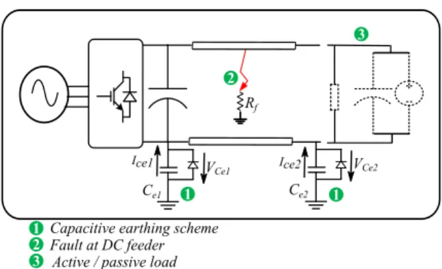
Fault location methods can be allocated into two main groups; active and passive. Active methods are based on signal injection (usually by deploying auxiliary equipment) to the faulted feeder, followed by the analysis of the reflected signatures. Passive fault location methods are solely based A. Makkieh, V. Psaras, R. Pe˜na-Alzola, D. Tzelepis and G. Burt are with the Institute for Energy and Environment of the Department of Electronic and Electrical Engineering at the University of Strath-clyde, 16 Richmond St, Glasgow G1 1XQ. Scotland, United Kingdom. e-mail:{ahmad.makkieh, vasileios.psaras, rafael.pena-alzola, dimitrios.tzelepis, graeme.burt}@strath.ac.uk. A. Emhemed is with the WSP consultancy limited, 110 Queen Street, Glasgow, G1 3BX, United Kingdom. e-mail:[email protected]. Ice1 Ice2 Rf Ce1 VCe1 Ce2
Capacitive earthing scheme Fault at DC feeder Active / passive load 1 2 3 4 1 2 3 VCe2 1
Fig. 1: DC microgrid feeder integrating multiple capacitive earthing scheme.
on the collection and analysis of measurements (either local and/or remote). Furthermore, fault location methods can be classified into offline (where the distance to fault is calculated after the fault has been cleared) and online methods (where the distance to fault is calculated while the fault evolves).
An active fault location method is proposed in [6] where the fault is located by injecting a DC voltage into the faulted feeder. The method utilizes a probe unit and a model of the RLC circuit to extract both the oscillation frequency and the attenuation coefficient to allow an estimation of the distance to the fault. Such a method has been improved by the work introduced in [5], [7] by specifically considering the impact of the attenuation coefficient on the accuracy of the fault location calculations.
Passive fault location methods based on single-ended elling waves are proposed in [4], [8]. Even though trav-elling waves have been widely used for fault location on transmission-level applications (i.e on high voltage DC grids with long transmission lines [9]), their utilisation in DC microgrids can prove challenging due to the small surge reflection time that can degrade the reliability and accuracy of the estimation [10].
A differential, current-based fast detection and fault location method is reported in [11]. The method relies on current measurements captured from both ends of the faulted feeder and utilizes a non-iterative and cumulative sum average ap-proach. Communication-based methods are associated with additional costs for the communication infrastructure and reli-ability concerns in the case of a failure in the communication link. To eliminate the communication requirements, a method is proposed in [12] which utilizes the least square method and boundary inductance. However, this method is applicable for radial DC networks but not for meshed DC networks
which can accommodate bidirectional power flows. Other fault location methods are proposed in [13], [14], which deploy local voltage and current measurements. These methods are not tested in networks where numerous converter-interfaced loads and DC sources are connected at both ends of the feeders, which are anticipated to change the fault current signatures during faults.
To address the aforementioned issues, this paper proposes a passive and communication-less fault location method. Furthermore, this method does not require additional signal injection and is applicable to any type of feeder termination, allowing for both passive connections as well as converter-interfaced loads and sources with DC-link capacitors. The method involves using a multiple capacitive earthing scheme, connected at the negative pole of the DC cable for a two wire (unipolar) system (refer to Fig. 1 for a representative de-sign) combined with local voltage and current measurements. Moreover, the proposed method can operate for all kinds of systems topologies including a ring type DC microgrid as long as placing a capacitive earthing scheme in each bus. In this paper, the parasitic capacitances of the cable are neglected as their size is much smaller compared to that of the actual earthing capacitors. A reasonable model can thus be achieved. The paper is organized as follows. Section II presents the implementation of the capacitive earthing scheme in a DC microgrid. In Section III, the proposed fault location method is analysed in detail. The case studies and simulation results are presented in Section IV, followed by experimental results in Section V. Finally, the conclusions of the presented work are drawn in Section VI.
II. IMPLEMENTATION OF CAPACITIVE EARTHING SCHEME A multiple capacitive earthing scheme has been proposed for DC microgrids in order to prevent DC current leakage in the protective earthing conductor (under normal operating conditions) and also to form a conducting fault path during DC pole-to-earth faults [15], [16]. In a practical sense, such a scheme helps to minimize corrosion at adjoining infrastructure. During fault conditions, capacitors within such an earthing scheme are being charged by transient currents which are correlated with fault distance and fault resistance. Therefore, by assessing the response of the scheme during the fault, the distance to the fault can be estimated.
A. Steady state condition
During steady state operation, the use of a capacitive earthing scheme means the impedance to earth is infinite. As a direct consequence of this, the flow of DC earth current can be restricted, preventing corrosion. Alternatively, for high frequencies, the capacitor impedance decreases and hence, acts as a low resistance earthing scheme for fast transients.
B. Fault response
In the event of a pole-to-earth fault, the fault current will circulate through the capacitive earthing.
Fig. 2 illustrates a simplified representation of the capacitive earthing scheme during a pole-to-earth fault and the corre-sponding voltage and current signatures across the capacitor. At t = 1 ms the switch, S, closes (i.e. fault is triggered) and current flows into the capacitor (it is considered that the capacitor, Ce, is initially discharged). The resistor, Rf,
represents the fault resistance and the charging behaviour of the capacitor is described in (1) and (2):
0 1 2 3 4 −600 −400 −200 0 Time [ms] I [A] Ice 0 1 2 3 4−600 −400 −200 0 a) Time [ms] V [V] Vce Ice S Rf Ce Vnom Ice Vce + -b)
Fig. 2: Capacitive earthing scheme under pole-to-earth fault: a) Voltage and current signatures, b) Simplified circuit representation.
Vce(t) =Vnom 1−e−τt , τ =RfCe (1) ice(t) =Ce d dtVce= Vnom Rf e −t τ (2)
where,Vce, is the voltage across the earthing capacitor,Vnom,
is the nominal voltage of the supply network, ice, is the
current flowing through the earthing capacitor and τ is the time constant.
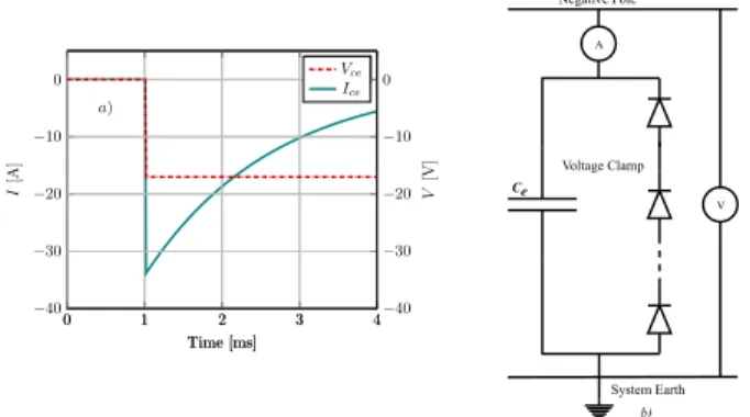
C. Voltage clamping
The charging of the DC capacitor is anticipated to cause voltage swings in the circuit. It is thus necessary to clamp the voltage to prevent the complete charging of the DC capacitor. For this purpose, a voltage-clamping diode is added in parallel with the capacitive earthing as shown in Fig. 3. An equivalent voltage clamping scheme can be made of a string of series-connected diodes, series-connected in parallel with the earthing capacitors. When a fault occurs in the network, the earthing capacitors will keep charging for the time window where the fault remains uncleared.
0 1 2 3 4 −40 −30 −20 −10 0 Time [ms] I [A] Ice 0 1 2 3 4−40 −30 −20 −10 0 a) Time [ms] V [V] Vce Ice A V Ce Negative Pole System Earth Voltage Clamp b)
Fig. 3: Voltage clamping scheme: a) Voltage and current signatures, b) Equivalent circuit.
By adding a voltage clamping-diode, the voltage across the earthing capacitor is controlled. Once the voltage across the
capacitor reaches the clamp voltage, the diode starts conduct-ing and prevents the voltage from risconduct-ing any further. While the diode is conducting, the system is earthed by an equivalent resistance earthing scheme (i.e. diode provides a low-resistive conduction path). For the studies presented in this paper, the clamp voltage is defined based on the assumption that the biggest allowable deviation on the poles is 2.5% of the nominal voltage (i.e. 750V), in this case, ±18.75V.
D. Capacitor sizing
Sizing the earthing capacitor correctly is important in pro-viding the protection device enough time to isolate the fault before the capacitor reaches clamp voltage. This ensures that the voltage-clamping diode does not conduct during the fault. It is therefore desirable to keep the earthing capacitors charged in the network to prevent the occurrence of this phenomenon. With the aid of the IEC 60479-1 standard, which defines the maximum trigger time of protection operation [17], the size of the earthing capacitors of the network are calculated. The following assumptions have been considered to calculate the size of the earthing capacitors:
• The maximum resistance of the fault path is chosen to be the upper value of the body impedance; 1050Ω. Note that this value of maximum fault path resistance does not affect the proposed algorithm introduced later in the paper and is only used in sizing the earthing capacitor.
• The total inductance value of the fault loop depends on the location of the fault. A higher inductance value will lead to a lower di/dtof the fault current. Therefore, it is neglected in order to derive a more conservative value for the size of the earthing capacitors.
• The voltage across the fault depends on the load con-nected to the faulted pole and is considered to be the nominal pole voltage.
• The maximum fault current is used for the calculation. Using (2) and considering Vnom=Vf and Vce=Vclamp, the
size of the earthing capacitors can be calculated as follows [18]: C=−tmaxR f ln 1−VclampV f −1 (3)
where Vclamp is the clamp voltage, Vf is the voltage across
the fault, and tmax is the maximum time for the protection
to operate. From the calculation shown in Table I, the total capacitance is 10 mF for the entire network. Therefore, the individual earthing capacitor can be calculated as follows:
CeIndividaul =
C
N (4)
where C is the total capacitance and N is the number of earthing points. In this paper, three earthing points are considered and therefore the size of the each earthing capacitor is 3.3 mF.
TABLE I: Values used for earthing capacitor sizing.
Vf If Rf tmax Vclamp C [V] [A] [Ω] [S] [V] [F] 750 0.250 1050 0.25 18.75 0.010
III. PROPOSED FAULT LOCATION METHOD
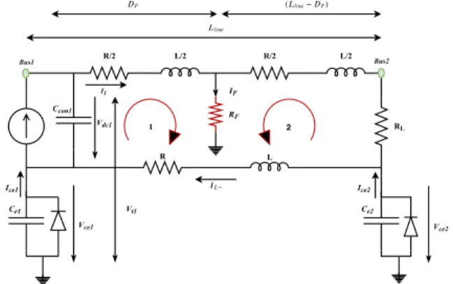
The proposed fault location method is based on the ana-lytical derivation of the system’s state space equations during fault conditions. The model is derived with reference to Fig. 4, which illustrates a fault occurring at the middle of the feeder (fault position is denoted by DF) with earthing capacitors
connected at both ends of the negative pole of the feeder. The derived model, combined with local measurements of voltage and current from buses 1 and 2 (sampled at 100kHz), are used to determine the fault position,DF, along the feeder.
Vce1 1 2 Ce1 Ice1 Ccon1 RL Vce2 Ce2 RF L R R/2 L/2 R/2 L/2 I1 − ( − ) IF Ice2 Vdc1 Vt1 Bus1 Bus2
Fig. 4: Equivalent network of DC feeder with DC source, load and multiple capacitive earthing scheme. Fault occurs atDF=50% of the feeder’s length in the shown case.
A. Faulted feeder model
The state space equations, which reflect the feeder termi-nal voltages under the influence of a pole-to-earth fault (as depicted in Fig.4), are written as:
Vce1 +Vdc1 =L1 d dti1(t) +i1R1+ (i1+ice2)Rf (5) Vce2 =ice2RL+ (i1+ice2)Rf+ice2 (RT −R1) + d dtice2(t)(LT−L1) (6) whereL1, R1 are the equivalent cable inductance and
resis-tance up to the fault point (taking as reference Bus1), Rf is
the fault resistance,LT andRT are the total inductance and
resistance of the feeder,Vdc1is the voltage across the filtering
capacitor at Bus1, Vce2 is the voltage across the earthing
capacitor at Bus 2,i1 is the line current from Bus1 and ice2
is the earthing capacitor current at Bus2 during the fault. In the case of the pole-to-earth fault, the feeder parameters can be written in terms of the relative fault distance,m:
where m=DF/Lline is the ratio between the actual fault
distance and the total length of the feeder. Subtracting (6) from (5) and substitutingL1,R1 andmfrom (7) gives:
Vce1+Vdc1 −Vce2 =mLT d dti1(t) +i1mRT −ice2RL −ice2(RT−mRT)− d dtice2(t)(LT −mLT) (8) As the fault evolves, the earthing capacitorsCe1andCe2are
being charged through the fault current, until voltage clamping starts. In the meantime, filtering capacitors Ccon1 andCcon2
are being discharged, contributing to the overall fault current. Current, ice2, flowing through earthing capacitor,Ce2, during
the fault transient, is related to Vce2as:
Vce2 = Rt
0ice2dt
Ce2
(9) Substituting Vce2 from (9) in (8) gives:
Vce1 +Vdc1 − Rt 0ice2dt Ce2 =mLT d dti1(t) +i1mRT −ice2RL −ice2 (RT −mRT)− d dtice2(t)(LT −mLT) (10) Rearranging equation (5) in terms of ice2 and substituting
the resulting relationship in (10) yields :
G1m2+G2m+G3Rf+J =Y∗ (11)
where J is an integration constant and G1, G2, G3 andY∗
are coefficients, given by: G1=RT2i1+ 2LTRT d dti1+LT 2d2i1 dt2 (12) G2= −LT2 d2i 1 dt2 −RLLT d dti1−2LTRT d dti1 −RLRTi1−RT2i1−LT d dtVt1 −RTVt1+ LT R t 0i1dt Ce2 +RT Rt 0i1dt Ce2 (13) G3=−LT d dti1−RLi1−RTi1+ Rt 0i1dt Ce2 +Vt1 (14) Y∗= −RLVt1 −RTVt1 −LT d dtVt1 − Rt 0Vt1dt Ce2 (15) Equation (11) is used in the proposed method to determine the values of the cable fault distance, m, and fault resistance, Rf. In the case of multiple sources as shown in Fig. 5,
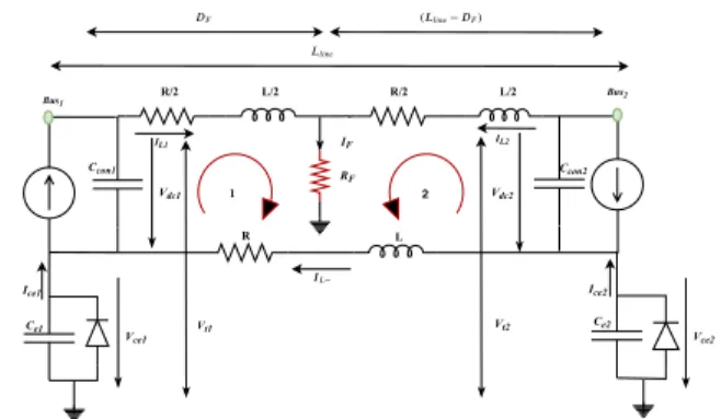
equa-tions (5) and (6) are applicable by performing the following amendments:
• Replace (Vce2 +Vdc2)withVt2
• iL1 becomes the total fault current flowing from Bus1 • iL2 becomes the total fault current flowing from Bus2
1 2 Ce1 Ice1 Vce2 Ce2 Ice2 RF L R R/2 L/2 R/2 L/2 IL1 − ( − ) IF Ccon2 IL2 Vdc1 Vdc2 Vt1 Vt2 Ccon1 Vce1 Bus1 Bus2
Fig. 5: Equivalent network of DC feeder with DC sources at both terminals and multiple capacitive earthing scheme. Fault occurs at
DF=50% of the feeder’s length.
B. Fault location procedure
The proposed fault location method consists of three main stages as depicted in Fig. 6 and is explained in detail as follows:
1) Stage I: Signal acquisition and coefficient calculation:
At this stage, all the signals required for the implementation of the fault location method are captured and the corresponding coefficients (i.e.G1,G2andG3) are calculated. When a fault occurs on the feeder, the current flowing from the earthing capacitor to the fault point becomes higher than the normal value. The proposed fault location algorithm then captures the local post-fault voltage and current traces associated with the earthing capacitor and the converter. Coefficients G1 to G3
andY∗are calculated at each time interval,∆t. Equation (16)
is constructed with selected sets of ten sampling points(N = 10), where the elements ofY∗ are the output coefficients and
the elements ofG1toG3 are the input coefficients. The term Y is defined as a prediction term in order to estimate the unknown values of variablesmandRf. The proposed method
considers a signal sampling rate of 100 kHz. This is because, the algorithm needs an elevated number of samples for the minimum square estimation gathered in the short time allowed by the capacitor charging. However, it must be considered that the only real-time process is gathering the samples and converting the signals to digital using the Analogue-to-Digital Converter (ADC), and storing the data in memory.
Y∗(t) Y∗(t+ ∆ (t)) .. . Y∗(t+N∆ (t)) = m2 m R f G1(t) G2(t) G3(t) G1(t+ ∆ (t)) G2(t+ ∆ (t)) G3(t+ ∆ (t)) .. . ... ... G1(t+N∆ (t)) G2(t+N∆ (t)) G3(t+N∆ (t)) (16)
2) Stage II: Fault location and resistance estimation:
At this stage, estimations of the fault location, m, and the fault resistance,Rf, are provided. The problem is formulated
and solved as an optimisation problem using non-linear pro-gramming. In particular, the objective function (referring to equations (17) and (18)) constitutes a minimisation problem whereby the sum of the square errors (or residuals) between the prediction function, Y, and the calculated function, Y∗,
within the selected dataset, should be minimised (estimates of variablesmandRf are provided by deploying the non-linear
programming function-f mincon). Obj =X Y −Y∗ Y∗ 2 (17) X(m,Rf)=fmincon(Obj, X0) (18)
whereX is a two-dimensional scalar containing estimates of both fault location and its fault resistance,Objis the objective function, and X0 is an initial value.
The f mincon function has been deployed from the MAT-LAB optimisation toolbox and the tolerance of the objective function, step, and optimality were chosen as 1e−6.
3) Stage III: Fault location evaluation: This is the last stage of the proposed method, where the fault location is reported according to a reliability criterion. During the assessment of the proposed fault location algorithm, it has been observed that the solver might provide infeasible solutions after a certain fault location, m. From the mathematical point of view, the sign of function Y∗ has an impact on the operation of the
solver for obtaining the feasible solutions. More specifically, when the function Y∗ becomes negative, the reliability of the
solver is compromised. As a result, an adjustment is made so that when Y∗ is negative, the term 1
−m replaces min the algorithm to restore correct operation.
IV. SIMULATION RESULTS
A. Study network and methodology
The system under study is a typical DC microgrid network as depicted in Fig. 7 (the corresponding system parameters are illustrated in Table II). The DC network is connected to an AC grid supply point through a two-level VSC and a transformer at Bus 1. DC-DC converters are connected at Bus 2 to integrate the Battery Energy Storage System (BESS) and solar PV system. A lumped DC load is connected at DC Bus 3. A capacitive earthing scheme is connected to Bus 1, Bus 2 and Bus 3. A pole-to-earth is applied at different locations whereas the pole-to-pole events are not considered in this study. Ref [16] studies the latter cases and as the capacitors provide an instantaneous path to ground, they exhibit a similar response to pole-to-earth faults (i.e. Vdc to true earth).
Fault Location Estimators (F LE), where measurements are collected and algorithm executed, are positioned at Bus 1 and Bus 2 respectively. The fault location results presented in this paper consider F LE1 and F LE2 respectively. The values
of fault location estimation error reported in the following subsections have been calculated according to (19):
Stage II
Read voltage and current measurement
Ice > th ?
Populate matrix G and Y* Define effective window for G1,G2,G3,Y* Non-linear optimization process (Fmincon) Define prediction function Y and initial
guess values Define objective function Stage III m Minimization criteria satisfied
Report fault location on the feeder
Y*< 0 ?
Do
(1 − )
Report fault location on the feeder
Y N
Estimate m and Rf with define effective
window
Stage I
Fig. 6: Flow chart of the proposed fault location algorithm.
DC/DC Buck-Boost Converter VSC DC Load Battery Storage System 11 kV/0.4kV 1MVA M V G ri d S u p p ly Solar Panel 750V DC DC/DC Boost Converter DC Microgrid Network Bus 1 Bus 2 Ce1 Ce2 F2 F1 FLE1 FLE2 Ce3 Bus 3 DC cable 1 (1 km) DC cable 2 (1 km)
Fig. 7: Representation of DC microgrid.
errorm(%) = mLline−DF
Lline
.100% (19) wheremLlineis the calculated fault distance,DF is the actual
fault distance andLlineis the total length of the faulted cable.
Similarly for fault resistance, Rf, the error reported in the
following subsections have been calculated according to (20):
errorRf(%) =
Rf−Rf(a)
Rf(a)
.100% (20)
where Rf is the calculated fault resistance and Rf(a) is the
TABLE II: AC and DC Network Parameters
Parameter Value
AC grid Voltage [kV] 11 Transformer voltage ratio [kV] 11/0.4
DC voltage [V] 750 R, L of LVDC cable 0.017204 [Ω/km],3.3 [mH/km] [19] Earthing capacitor[mF] 3.3 Battery rating [kWh] 7.8 PV rating[kW] 10 DC load[kW] 19
B. Fault distance estimation for cable between DC sources and passive DC Load
In this case the proposed fault location method is tested for a cables are connected between DC sources and passive DC loads (i.e. reflecting the effect of increasing the fault resistance). A fault, F1, as shown in Fig.7 is triggered at DC
cable connecting Bus 2 and Bus 3 at different fault locations and fault resistances. The relative error in the fault distance estimated by theF LE2is given in Table III. By observing the
values in Table III , it can be demonstrated that the accuracy of the proposed method is satisfactory (i.e. the maximum error is -0.402%).
TABLE III: Distance estimation errors for faults at DC cable 2.
Distance Rf=0.1 Rf=0.5 Rf=1.0 Rf=1.5 Rf=2.0 [km] Ω Ω Ω Ω Ω 0.05 -0.0197 -0.0792 -0.1391 0.2209 -0.4022 0.1 -0.0273 -0.0835 -0.1445 -0.1878 -0.1956 0.2 -0.034 -0.084 -0.139 -0.185 -0.219 0.3 -0.032 -0.077 -0.127 -0.166 -0.195 0.4 -0.016 -0.054 -0.099 -0.142 -0.18 0.5 -0.005 -0.046 -0.094 -0.137 -0.175 0.6 -0.003 -0.045 -0.094 -0.138 -0.179 0.7 -0.003 -0.047 -0.1 -0.15 -0.196 0.8 -0.003 -0.053 -0.114 -0.172 -0.227 0.9 -0.003 -0.06 -0.128 -0.194 -0.258 0.95 -0.003 -0.06 -0.13 -0.197 -0.262
There is, however, a general trend that as the fault resistance increases, the current waveforms become smoother and the persistent excitation signals for minimum square algorithm are diminished, hence the level of accuracy in the estimation deteriorates. Moreover, the total inductance of the feeder is small compared to the large fault resistance. As a result, the calculation errors for fault distance increase when the fault resistance dominates system response.
Similar results have been observed for the fault resistance estimation as depicted in Fig. 8. It is observed that F LE2
estimates the fault resistance with less than -1% error, however, the calculation errors for fault resistance decrease when the fault resistance dominates the system response. Hence, the corresponding error for a fault at 0.95 km and Rf=2 Ω is
-0.28 %.
C. Fault distance estimation with multiple DC sources
In order to test the proposed fault location method in cases where DC sources are connected at both cable terminals (i.e. to consider the effect of the in-feed transient current generated from both DC converters during a fault), a fault (i.e.F2) has
-1 1 -0.8 0.8 -0.6 2 Error Rf (%) -0.4 0.6 1.5 Distance (km) -0.2 Rf ( ) 0.4 1 0 0.2 0.5 0 0 -0.9 -0.8 -0.7 -0.6 -0.5 -0.4 -0.3 -0.2 -0.1 0 0.1
Fig. 8: Relative errors for fault resistance estimation for faults at DC cable 2.
been triggered along the DC cable connecting Bus 1 and Bus 2 (refer to Fig.7) for varying fault location and resistance values. It is noticed that a large error in distance estimation is provoked when a fault occurs beyond a certain point of the total cable length. This is because the influence of the calculated output coefficient,Y∗, on the optimisation function,
X. Therefore, in order to investigate the influence of the calculated output coefficient, Y∗, on the estimation results,
the current flow through the inductor, the voltage derivative and the calculated output coefficient values are compared for four different fault locations on the cable, (i.e. fault at 10%, 30%, 50%, and 90% of the total cable length) as shown in Fig. 9. 0 1 2 3 4 5 6 7 0 0.5 1 1.5 a) IL [kA] DF=10% DF=30% DF=50% DF=90% 0 1 2 3 4 5 6 7 0 200 400 b) dv /dt [kV/s] 0 1 2 3 4 5 6 7 −1 0 1 c)
time window of interest
Time [ms]
Y
∗
[kV]
Fig. 9: System response for faults along various point on the cable: a) CurrentIL, b) Voltage derivative dV
dt, c) Output calculated coefficient
Y∗.
The fault current magnitude is reduced as the fault moves away from the measurement point as shown in Fig. 9(a). Also, it is observed that the magnitude of the rate of change of voltage varies with the fault location, as shown in Fig.9(b).
This is because the closest capacitors supply the majority of the fault current. Consequently, the magnitude of the output coefficient, Y∗, varies with respect to the magnitude of the
voltage derivative dv/dt (i.e. the rate of change of the sum of the voltage across the DC linkVdc1 and the voltage across
the earthing capacitorVce1) in accordance with (15) as shown
in Fig. 9(c). Moreover, due to the squared magnitude in the objective function that effects the estimation results after 50% of the total cable length, another criterion (i.e. the sign of the output coefficientY∗) is used to determine the valid function.
Accordingly, an adjustment is made for the fault distance estimation after 50% of the total cable length so that when Y∗ is negative, the term(1−m)replacesmin the algorithm
to restore correct operation. Hence, the relative errors in the estimations performed by F LE1 for various faults are shown
in Table IV.
TABLE IV: Distance estimation errors for faults at DC cable 1.
Distance Rf=0.1 Rf=0.5 Rf=1.0 Rf=1.5 Rf=2.0 [km] Ω Ω Ω Ω Ω 0.05 -0.015 -0.071 -0.136 -0.199 -0.254 0.1 -0.014 -0.056 -0.101 -0.135 -0.156 0.2 -0.002 0.029 0.099 0.203 0.352 0.3 0.035 0.281 0.693 1.241 1.969 0.4 0.18 1.284 1.362 1.741 1.932 0.5 -0.042 -0.258 -0.539 -0.88 -1.308 0.6 -0.235 -1.881 -1.007 -1.252 -1.016 0.7 0.148 -0.553 -0.789 -0.61 -1.983 0.8 0.048 0.841 0.857 0.177 0.466 0.9 0.898 0.686 0.339 0.127 0.706 0.95 -1.164 -1.910 -1.450 -1.151 -0.891
Similar results have been observed for the fault resistance estimation as depicted in Fig. 10. It is observed that F LE1
estimates the fault resistance, Rf, accurately for the faults
closer to fault location estimator point. This is because, when the fault occurs close to the estimator point, the effect of the in-feed transient fault current from the remote end is less than that of a fault that occurs close to the remote side (i.e. fault at 60%, 70%, and 90%). Hence, The maximum error obtained for the fault resistance estimation, as expected at 0.95 km, is 6.5% for an expected fault resistance ofRf=2Ω.
-2 1 0 0.8 2 2 Error Rf (%) 0.6 4 1.5 Distance (km) 6 Rf ( ) 0.4 1 0.2 0.5 0 0 -2 -1 0 1 2 3 4 5 6
Fig. 10: Relative errors for fault resistance estimation for faults at DC cable 1.
Simulation results (Table III, Table IV) show the difference between the estimation errors that are performed by devices F LE1 andF LE2.F LE1 is connected between multiple DC
sources (i.e. power electronics converters with DC link capac-itors) where the fault current contributions of both converters changes the fault current signatures during events. Conversely, F LE2 considers the damped fault response (shown in Table
III) as the fault resistance increases. Hence the influence of these converters is the key factor for different error estimation. Moreover, the performance of the proposed algorithm has been scrutinized against highly resistive faults which can, notably, include gradually-evolving faults.
V. PRACTICAL VALIDATION OF THE PROPOSED FAULT LOCATION METHOD
In order to test the practical feasibility of the proposed fault location method, a scaled DC laboratory demonstrator has been utilized for replicating fault transients.
A. Experimental setup
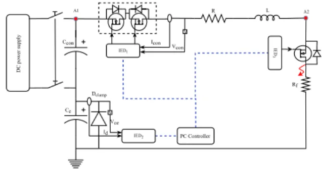
The DC microgrid depicted in Fig.7 has been simplified and scaled using the low-power test demonstrator as shown in Fig.11 (a photograph of the actual experimental layout is pre-sented in Fig.12). The main Voltage Source Converter (VSC) and the associated filtering capacitor (DC link capacitor) are represented by using a DC source in parallel with a capacitor (as shown in Fig. 11), which is used in this experiment to supply transient fault current. The capacitor earthing is connected in parallel with a Transient Voltage Suppression (TVS) diode at the negative pole. The TVS device will conduct to its fully rated current when it reaches the clamping voltage, in this experiment this is selected to be 6.8 Vdc. The DC voltages and currents are measured using Hall-effect sensors [20]. Two antiparallel MOSFETs are used as a solid-state DC breaker and act to clear the fault-currents. The fast ground-faults are created artificially by controlling the gate driver [21] of a MOSFET that connects the DC cable directly to ground. All the measuring sensors are interfaced to the Intelligent Electronic Devices (IEDs) which are emulated on a National Instrument (NI) CRIO-based FPGA [22] that is used for data logging as well as generating the gate signals to turn-on or turn-off the MOSFETs. The parameters of the hardware used for the experimental setup are given in Table V.
DC power supply V IED1 IED2 V R L Icon Ccon Vcon Ce Id Vce A1 A2 PC Controller Rf IED 3 Dclamp
Fig. 11: Schematic diagram of the experimental arrangement.
B. Experimental testing and results
The test circuit shown in Fig. 11 is energised at 15 Vdc, this value is selected due to the ready availability of a laboratory
8
Power supply
CRIO:hardware-software interface
Mimic of DC cable Capacitor earthing & diode
Filtering capacitor
Fig. 12: Laboratory experimental setup.
TABLE V: Circuit parameters of the experimental arrangement.
Vdc Ccon Ce M OSF ET Diode Rline Lline
[V] [mF] [mF] [Ω] [mH]
15 2.2 2.2 Rated 100 V/200 A 6.8 V 0.07 10
set-up for testing faults. A 10 mH inductance is selected to represent a fault distance that corresponds to a typical 3 km section of a DC cable. The fault resistance is set to 0.5 Ω
and a pole-to-earth fault is applied at the end of the DC cable as shown in Fig.11. The experimental results during this fault are presented in Fig.13. When the fault occurs at 0.1 ms, voltage across the filtering capacitor,Vdc, drops and
the current of the filtering capacitor, Idc, rises as shown in
Fig. 13(a). Consequently, the voltage across the capacitive earthing scheme increases, Vce, (refer Fig. 13(b)) until the
diode conducts (at approximately 5 ms) resulting in voltage clamping, at the moment the TVS diode is fully conducting. All the voltage and current traces associated with the earthing capacitor and the filtering capacitor are stored in memory and later in the data management streaming file. These measure-ments have been utilized and the corresponding coefficients (i.eG1,G2,G3andY∗ ) are calculated at each time interval
∆t. Consequently, these coefficients are assigned offline to the non-linear programming function f mincon to determine the fault distance and fault resistance. Alternatively, since the algorithm does not have significant real-time limitations, the algorithm could be included in the processor of a general protection system or use a dedicated microcontroller.
The fault distance and fault resistance are estimated by the fault location algorithm for the period after fault detection and before the diode starts conducting as shown in Fig.14. It is found that the corresponding error for a fault at 3 km and Rf=0.5 Ω is 3.1 %. As expected, the resulting accuracy of
the experimentally-calculated fault location is slightly lower than that obtained in simulation. This is mainly caused by the inaccuracy of the component parameters such as system noise and sensor measurements errors, which significantly affect the calculation of di/dtanddv/dt. Therefore, in order to verify the feasibility of the method, a moving average filter is used to filter the noise from the source, so that the location estimated error is kept to a low level. The algorithm
0 2 4 6 8 10 12 14 16 0 5 10 15 a) I [A] Vdc 0 2 4 6 8 10 12 14 16 0 5 10 15 V [V] Vdc Iconv 0 2 4 6 8 10 12 14 16 0 2 4 6 8
time window of interest b) Time [ms] I [A] Idiode 0 2 4 6 8 10 12 14 16 0 2 4 6 8 V [V] Vce Idiode
Fig. 13: Experimental results: a) DC Voltage and current of VSC filtering capacitor, b) Voltage across capacitive earthing scheme and diode current
accuracy could be improved by reducing the noise in the sensors and signal conditioning, which may incur additional costs. Experiments conducted by the authors demonstrate that the algorithm worked properly even with additional filtering. Hence, the proposed algorithm is considered to provide a reasonable trade-off between accuracy and implementation cost. The corresponding error calculated for the experimental-based signatures is 1.1 % (refer to Fig.14 ), demonstrating that the addition of filtering has ensured acceptable accuracy.
0 0.5 1 1.5 2 2.5 3 3.5 4 4.5 5 0 2 4 6 Time [ms] m [km] m 0 0.5 1 1.5 2 2.5 3 3.5 4 4.5 5 0 2 4 6 Time [ms] Rf [Ω] Rf m
Fig. 14: Fault distance and fault resistance estimation during experi-mental testing.
VI. CONCLUSIONS
Locating DC faults in DC microgrids still presents out-standing challenges. This paper proposes a new fault loca-tion method for a DC microgrid using a multiple capacitive earthing scheme. The proposed method operates entirely on local measurements (i.e voltages and currents) during the fault in order to estimate the fault location in real time. A mathematical model of a generic faulted feeder of a DC microgrid is derived and utilized by a fault location algorithm based on a non-linear optimisation method to accurately locate the fault and its associated fault resistance. Furthermore, the algorithm has the inherent property of estimating the fault distance successfully, regardless of whether a DC source or a DC load is connected at the remote end. The method has been shown to be reliable even for high levels of fault resistance. For a fault resistance of 2 Ω, the maximum percentage error estimated by F LE1 is -2% while the maximum percentage
error estimated by F LE2 is -0.4%. It is thus demonstrated
that the accuracy of the method remains uncompromised for a range of [0.1, 2] Ohms of fault resistance. Finally, the
feasibility of the proposed method is verified by a simplified DC microgrid laboratory model. Estimating the DC fault position within the faulted feeder in a DC network, consisting of multiple sources connected to different feeders, with such accuracy and reliability, offers the potential for quick system restoration. Consequentially, and crucially, this reduces time-consuming maintenance, particularly at times of distress, that ultimately serves to enhance the resiliency of a DC microgrid.
ACKNOWLEDGMENT
This work has been supported through the Engineering and Physical Sciences Research Council (EPSRC) Centre for Doctoral Training in Future Power Networks and Smart Grids (EP/L015471/1)
REFERENCES
[1] Q. Deng, “Fault protection in dc microgrids based on autonomous operation of all components,” Ph.D. dissertation, University of South Carolina, Columbia , USA, 2017.
[2] R. M. Cuzner and G. Venkataramanan, “The status of DC micro-grid protection,” inConf. Rec. - IAS Annu. Meet. (IEEE Ind. Appl. Soc., 2008. [3] A. Makkieh, R. Pena-alzola, A. Emhemed, G. Burt, and A. Junyent-ferre, “Capacitive earthing charge-based method for locating faults within a DC microgrid,” in2019 IEEE Third International Conference on DC Microgrids (ICDCM), May 2019, pp. 38–44.
[4] S. Azizi, M. Sanaye-Pasand, M. Abedini, and A. Hasani, “A traveling-wave-based methodology for wide-area fault location in multiterminal dc systems,”IEEE Transactions on Power Delivery, vol. 29, no. 6, pp. 2552–2560, Dec 2014.
[5] R. Mohanty, U. S. M. Balaji, and A. K. Pradhan, “An accurate non-iterative fault-location technique for low-voltage dc microgrid,”IEEE Transactions on Power Delivery, vol. 31, no. 2, pp. 475–481, April 2016.
[6] J. Park, J. Candelaria, L. Ma, and K. Dunn, “Dc ring-bus microgrid fault protection and identification of fault location,”IEEE Transactions on Power Delivery, vol. 28, no. 4, pp. 2574–2584, Oct 2013. [7] R. Mohanty, U. S. M. Balaji, and A. K. Pradhan, “An accurate
non-iterative fault location technique for low voltage dc microgrid,” in2016 IEEE Power and Energy Society General Meeting (PESGM), July 2016, pp. 1–1.
[8] O. M. K. K. Nanayakkara, A. D. Rajapakse, and R. Wachal, “Traveling-wave-based line fault location in star-connected multiterminal hvdc systems,” IEEE Transactions on Power Delivery, vol. 27, no. 4, pp. 2286–2294, Oct 2012.
[9] D. Tzelepis, G. Fusiek, A. Dyko, P. Niewczas, C. Booth, and X. Dong, “Novel fault location in MTDC grids with non-homogeneous trans-mission lines utilizing distributed current sensing technology,” IEEE Transactions on Smart Grid, vol. 9, no. 5, pp. 5432–5443, Sep. 2018. [10] J. Suonan, S. Gao, G. Song, Z. Jiao, and X. Kang, “A novel
fault-location method for hvdc transmission lines,” IEEE Transactions on Power Delivery, vol. 25, no. 2, pp. 1203–1209, April 2010.
[11] S. Dhar, R. K. Patnaik, and P. K. Dash, “Fault detection and location of photovoltaic based dc microgrid using differential protection strategy,”
IEEE Transactions on Smart Grid, vol. 9, no. 5, pp. 4303–4312, Sep 2018.
[12] X. Feng, L. Qi, and J. Pan, “A novel fault location method and algorithm for dc distribution protection,”IEEE Transactions on Industry Applications, vol. 53, no. 3, pp. 1834–1840, May 2017.
[13] J. Yang, J. E. Fletcher, and J. O’Reilly, “Short-circuit and ground fault analyses and location in vsc-based dc network cables,” IEEE Transactions on Industrial Electronics, vol. 59, no. 10, pp. 3827–3837, Oct 2012.
[14] X. Feng, L. Qi, and J. Pan, “Fault inductance based protection for dc distribution systems,” in13th International Conference on Development in Power System Protection 2016 (DPSP), March 2016, pp. 1–6. [15] L. Mackay, K. F. Yanez Martinez, E. Vandeventer, L. Ramirez-Elizondo,
and P. Bauer, “Capacitive grounding for dc distribution grids with two grounding points,” in2017 IEEE Second International Conference on DC Microgrids (ICDCM), June 2017, pp. 76–80.
[16] A. Makkieh, A. Emhemed, D. Wong, G. Burt, and A. Junyent-ferre, “Fault characterisation of a dc microgrid with multiple earthing under grid connected and islanded operations,” in 2018 53rd International Universities Power Engineering Conference (UPEC), Sep. 2018, pp. 1– 6.
[17] IEC60479-1, “Effects of current on human beings and livestock - Part 1: General aspects,” 2005.
[18] E. Vandeventer, “Residual current protection of a meshed dc distribution grid with multiple grounding points,” Master’s Thesis, Delft University of Technology, Netherlands, 2016.
[19] K. A. Saleh, A. Hooshyar, and E. F. El-Saadany, “Hybrid Passive-Overcurrent Relay for Detection of Faults in Low-Voltage DC Grids,”
IEEE Trans. Smart Grid, 2017.
[20] LEM, “Current HAS50—600-S and Voltage Transducer-LV25-P.” [Online]. Available: https://www.lem.com/en
[21] Semikron, “Power mosfet modules-semitrans tm m1 skm111ar.” [Online]. Available: https://www.gdrectifiers.co.uk/uploads/SEMIKRON [22] N. Instrument, “Intelligent Real-Time Embedded Controller for CompactRio on FPGA Chassis and I/O modules.” [Online]. Available: http://www.ni.com/pdf/manuals/375233f.pdf
Ahmad Makkieh(S’15) received the B.Eng. (Hons)
degree in electrical, electronics and energy engineer-ing and the M.Sc degree in wind energy systems from Glasgow Caledonian University (2015) and University of Strathclyde (2016) respectively. He is currently pursuing his Ph.D. at the Department of Electronic and Electrical Engineering, University of Strathclyde, Glasgow, U.K. His main research interests include LVDC microgrid protection, fault location and control applications, and smart grids.
Vasileios Psaras (S’14) received the diploma
de-gree in electrical engineering from the University of Patras, Rion-Patras, Greece in 2014, and the M.Sc degree in wind energy systems from the Univer-sity of Strathclyde, Glasgow, UK, in 2016. He is currently pursuing his Ph.D. at the Department of Electronic and Electrical Engineering, University of Strathclyde, Glasgow, UK. His main research inter-ests include DC grid protection, fault location and advanced signal analysis for protection applications.
Rafael Pe ˜na Alzola(S08) (M15) (SM20) received
the combined licentiate and M.Sc. degree in indus-trial engineering from the University of the Basque Country, Bilbao, Spain, in 2001, and the Ph.D. degree from the National University for Distance Learning (UNED), Madrid, Spain, in 2011. He has worked as an electrical engineer for several compa-nies in Spain. From September 2012 to July 2013, he was Guest Postdoc at the Department of En-ergy Technology at Aalborg University in Aalborg, Denmark. From August 2014 to December 2016, he was Postdoc Research Fellow at the Department of Electrical and Computer Engineering at The University of British Columbia in Vancouver, Canada. From January 2017 to May 2017, he was with the University of Alcal´a in Madrid, Spain for a short-term industrial collaboration. Since June 2017, he is with the University of Strathclyde in Glasgow, UK initially as Research Fellow and since 2019, as a Lecturer at the Rolls-Royce University Technology Centre. His research interests are energy storage, LCL-filters, solid-state transformers, power electronics for hybrid electric aircraft and innovative control techniques for power converters.
Dimitrios Tzelepis(S13M17) received the B.Eng. (Hons) degree in electrical engineering from the Technological Education Institution of Athens, Athens, Greece, in 2013, and the M.Sc. degree in wind energy systems and the Ph.D. degree from the University of Strathclyde, Glasgow, U.K., in 2014 and 2017, respectively. He is currently a Postdoctoral Researcher with the Department of Electronic and Electrical Engineering, University of Strathclyde. His research interests lie within the area of power system protection, automation and control of future electricity grids, incorporating increased penetration of renewable energy sources and high voltage direct current interconnections. His main research methods include implementation of intelligent algorithms for protection, fault location and control applications including the utilisation of machine learning methods and advanced and intelligent signal processing techniques.
Abdullah A S Emhemed (M’07) received the
B.Eng. in electrical power systems from Nasser Uni-versity, Libya, MSc from University of Bath, U.K. (2005), and PhD. from University of Strathclyde, U.K. (2010). He is a full member of IEC LVDC Systems Committee and IET TC2.4 on LVDC. He is currently a principal power systems engineer at WSP, and his main areas of expertise include DC microgrids, and dynamic modelling and analysis of power systems and HVDC systems.
Graeme M. Burt(M95) received the B.Eng. degree
in electrical and electronic engineering, and the Ph.D. degree in fault diagnostics in power system networks from the University of Strathclyde, Glas-gow, U.K., in 1988 and 1992, respectively. He is cur-rently a Distinguished Professor of electrical power systems at the University of Strathclyde where he directs the Institute for Energy and Environment, directs the Rolls-Royce University Technology Cen-tre in Electrical Power Systems, and is lead aca-demic for the Power Networks Demonstration Cen-tre (PNDC). In addition, he serves on the board of DERlab e.V., the association of distributed energy laboratories. His research interests include the areas of decentralised energy and smart grid protection and control; electrification of aerospace and marine propulsion; DC and hybrid power distribution; experimental systems testing and validation with power hardware in the loop.