All Rights Reserved © 2012 IJARCSEE
100
Abstract
—
Many computation-intensive iteration or recursive application commonly found in digital signal processing and image processing applications uses digital filter as basic components. In this paper we focus on designing digital filter which confine a signal into a prescribed frequency band. The work concentrates at first on the development of the low pass finite impulse response (FIR) digital filter using Mat-Lab FDA tool then we designed the different methodologies for the implementation for the of the FIR filter. We have designed the broad cast structure and the overlap save method. We have tested our algorithm using the Xilinx synthesis tool and then implemented on Spartan 3 family xcs40001-4fg900 FPGA device. The experimental results shows that overlap save structure can be operated in less frequency of 57.382 MHz in comparison to the 155.569 MHz operating frequency of the broadcast structure.Index Terms— FIR, FPGA, MaT-Lab,LUT,DSP
I. INTRODUCTION
Digital signal processing (DSP) and media applications requires large computing power and have real-time performance requirements. The computing engine in such applications tends to be embedded as opposed to general purpose[1,2]. This paper concerns in designing digital filters, as the digital filter is the basic component of all signal processing and telecommunication system.
The general form of the digital filter difference equation is given by
(1)
Where Y(n) is the current filter outputs, the Y(n-k)’s are current or previous filter inputs, the ak’s are the filter’s feed
forward co-efficient corresponding to the zeros of the filter, the bk’s are the filter’s feedback co-efficient corresponding
to the pole of the filter, and N is the filter’s order. Depending upon the filter co-efficient there are two type of digital filter if the co-efficient are fixed then it is frequency selective filter and if the co-efficient updated at each iteration in order to minimize the difference between the filter output and the desired signal then it is a adaptive digital filter. The frequency selective filters are of two type infinite impulse response (IIR) and finite impulse response (FIR) digital filter. To design this low pass filter, we have used Mat-Lab FDA as the synthesis tool. Now for FPGA implementation of this digital filter, we have proposed broadcast structure and overlap-save method structure[3,4]. Broad-cast structure is the direct form structure of the FIR filter whereas the overlap save method is known as the block filtering scheme. These scheme converts large size FIR filtering into block filtering by segmenting input sequence into blocks and combine the output of block Sumit Kumar Maity , Madhusudan Maiti
A comparative study on FPGA based FIR filter
using broadcast structure and overlap save
method.
All Rights Reserved © 2012 IJARCSEE
101
filtering together to obtain the output of the original FIR filtering. The rest of the paper is organized as follows. Design of the low pass FIR digital filter is given in section 2. The FPGA implementation of the broad cast structure of FIR filter is shown in section 3. The FPGA implementation of overlap save structure is given in section 4. The comparison of optimization parameters are given in section 5. Section 6 shows the conclusion.
II. DESIGN OF FIR DIGITAL FILTER
We know frequency selective digital filter are of two type infinite impulse response (IIR) and finite impulse response (FIR). IIR filter have one or more non-zero feedback co-efficient that is as a result of the feedback term, if the filter has one or more poles, once the filter has been excited with an impulse there is always an output. FIR filter have no non-zero feedback co-efficient[5]. That is the filter has only zeros, and once it has been excited with an impulse, the output presents for only a finite (N) number of computational cycles. The difference equation of the FIR filter is given by
(2)
The output y(n) of this filter is a function of input signal x(n). The response of this filter to an impulse consists of a finite sequence of N+1 sample, where N is the order of the filter. We have designed a third order digital FIR filter using Mat-Lab FDA as the synthesis tool. The magnitude and phase plot of this filter is shown in figure 1. To design this FIR filter we have used the specification as given in the table 1, with the transfer function co-efficient given in the table 2.
I. Table
Properties Specification
response Low pass
order 3rd
stable Yes
window Rectangular window
Cut off frequency (wc) 0.25 (normalized) Attenuation at cut off
frequency
6db
II. Table
Transfer function Co-efficient
h(0) 0.3215
h(1) 0.3571
h(2) 0.3215
To design this filter we have used the rectangular window method. The general form of the rectangular window method is given by
III. IMPLEMENTATION OF THE FILTER USING THE BROADCAST STRUCTURE
From the difference equation of the FIR filter as given in equation (2) we can write the equation as
Y(n)=h(0)x(n)+h(1)x(n-1)+h(2)x(n-2) (4)
To implement this equation we have used the broad cast structure as shown in the figure 2. Here we have used the controlled shift register to implement the filter co-efficient, z-1 as the delay flip-flop, ripple carry adder for the different mathematical addition operation. For the FPGA implementation we have to approximate the filter co-efficient as shown in the table3.
III. Table
Input sequen ce
Binary equivalen t value of input sequence Actual value of output sequen ce Approxim ate value of output sequence
Binary equivalent value of output sequence
1.0 0001.000 00
0.3215 0.3203125 0000.01010 01
2.0 0010.000 00
1.0001 0.9921875 0000.11111 11
3.0 0011.000 00
2.0002 1.9921875 0001.11111 11
4.0 0100.000 00
3.0003 2.9765625 0010.11111 01
5.0 0101.000 00
4.0004 3.96875 0011.11111 00
6.0 0110.000 00
5.0005 4.9609375 0100.11110 11
7.0 0111.000 00
6.0006 5.953125 0101.11110 10
8.0 1000.000 00
7.0007 6.9453125 0110.11110 01
9.0 1001.000 00
8.0008 7.9375 0111.11110 00
All Rights Reserved © 2012 IJARCSEE
102
This filter is implemented in Spartan 3 family FPGA, with device specification XC3S40001-4fg900. The simulation waveform and the requirement of logical element is given in Figure 3 and Figure 4.
VI. IMPLEMENTATION OF DIGITAL FILTER USING OVERLAP SAVE METHOD
Filtering the real time long duration signal becomes computational intensive. Thus the scheme of block filtering is widely used. Overlap save method is a block filtering scheme. In this scheme the input sequence must be divided into blocks. The successive blocks are processed separately one at a time and the results are combined later to yield the desired output sequence which is identical to the sequence obtained by broad cast structure[6,7]. Let the length of the input sequence is L and the length of the impulse response is M. In this method the input sequence is divided into blocks of size N=L+M-1. Each block consist of last (M-1) data points of previous block followed by L new data points to form a data sequence of length N=L+M-1. For first block of data the first M-1 points are set to zero[8]. Thus the blocks of data sequence are
(5)
(6)
and so on.
Thus the output response is given by
Here yi(n) is the output blocks and it is computed by the
circular convolution of input blocks xi(n) and impulse
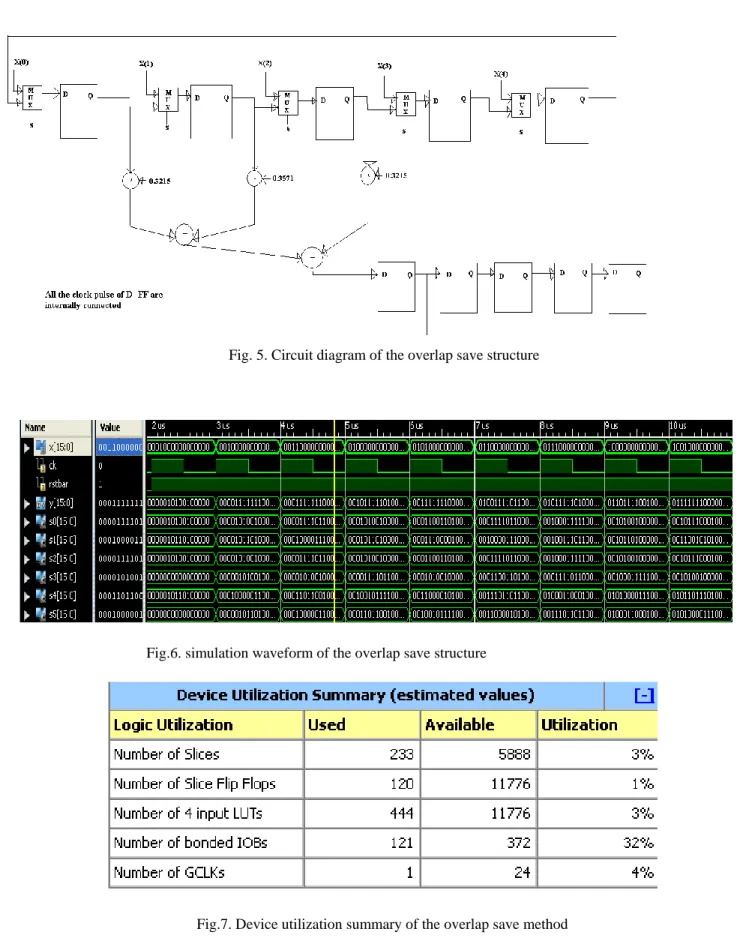
response h(n). The Figure 5 shows the circuit for the computation of the output response of digital filter using the overlap save structure. In this structure at first we select ‘S=0’, to load the input value in the flip flop and when the select line ‘S=1’ then the circular convolution process will take place. Simulations wave form and the requirement of logical element are given by Figure 6 and Figure 7. To implement this circuit we have used the controlled shift register to design the filter co-efficient, D-flip-flop for designing z-1 and ripple carry adder for the different mathematical addition operation.
Fig.3.Simulation waveform of the broadcast structure
All Rights Reserved © 2012 IJARCSEE
103
Fig. 5. Circuit diagram of the overlap save structure
Fig.6. simulation waveform of the overlap save structure
All Rights Reserved © 2012 IJARCSEE
104
V. CONCLUSION
In this paper, we have presented a model that can implement a FIR filter using both broadcast structure and overlap save method. The comparison of both the structure shows that in order to implement a high speed digital filter, we should use the overlap save structure as in this structure the minimum input arrival time before the clock is 3.166ns in comparison to 20.503 ns for the broadcast structure. Similarly we find that in overlap save structure output require time after clock is 5.558 ns in comparison to the 21.808ns for the broadcast structure.
REFERENCES
[1]Liang-Fang Chao Edwin Hsing-Mean Sha ―unfolding andretiming data flow DSP Program for RISC multiprocessor scheduling” IEEE International Conference on Acoustics,Speech, and Signal Processing, 1992. ICASSP-92 Vol 5, 1992.
[2]TimothyW. O„Neil Edwin H.-M. Sha ―Rate optimal graph transformation via Extended retiming and unfolding‖,
Proceedings of the IASTED International ConferenceParallel and Distributed Computing and Systems (PDCS ’99) Nov 3-6,1999 – Cambridge, MA, USA.
[3] Qingfeng Zhuge, Chun Xue, Zili Shao, Meilin Liu,‖Design optimization and space minimization considering timing andcode size via retiming and unfolding” Microprocessors
andMicrosystems, Volume 30, Issue 4, Pages 173-183, 6 June
2006.
[4] Timothy W. O'Neil , Edwin H.-M. Sha ―Combining Extended retiming and unfolding for rate optimal graph transformation‖ Journal of VLSI Signal Processing Systems,Volume 39 Issue 3, March 2005.
[5] T. W. O'Neil , and E. H.-M. Sha ―Optimal graph transformation using extended retiming with minimal unfolding‖ in the Proceedings of the IASTED International Conference on Parallel and Distributed Computing Systems, Las Vegas, NV, November, 2000, pp. 128-133.
[6]José Monteiro, Srinivas Devadas, Abhijit Ghosh‖Retiming sequential circuit for low power‖ Proceedings of the IEEE/ACM international conference on Computer-aided design, ICCAD '93.
[7] Santosh Chede , Kishore Kulat , Rajesh Thakare ―A significance of VLSI Technique for low power real Time system‖ 2010 International Journal of Computer
Applications(0975 - 8887),Volume 1 – No. 22.
[8] Mandeep Kaur, Vikas Sharma ―Analysis of various algorithm for low power consumption in embedded system using different architecture‖ International Journal of Electronics Engineering, 2(1), 2010,
Prof.Sumit Kumar Maity obtained his M.Sc. degree in Electronics in 2003 from the Vidyasagar Universiy. He worked as a Lecturer in the Vivekananda Mission
Mahavidyalay, Haldia during 2004- 2006. At present he is a lecturer at department of Electronics , Jogesh Chandra Chandra Chaudhuri College, Kolkata. His research interest includes Digital Signal Processing , Embedded systems and Digital Electronics circuit. He has a number of research papers in well- known journals.
Prof.Madhusudan Maiti obtained his M.Sc. degree in