ISSN(Online): 2320-9801
ISSN (Print): 2320-9798
International Journal of Innovative Research in Computer
and Communication Engineering
(An ISO 3297: 2007 Certified Organization)
Vol. 3, Issue 6, June 2015
Optimization and Return loss Reduction
Of Micro strip Patch Antenna
Jinal R. Patel
1, Jigar B. Chaudhari
2PG Student, Dept. of E&C Engineering, Sakalchand Patel College of Engineering, Visnagar, Gujarat, India1
Assistant Professor, Dept. of E&C, Sakalchand Patel College of Engineering, Visnagar, Gujarat, India2
ABSTRACT: An Antenna is one of the essential parts for microwave communication. Since it help both transmitting
and receiving the information. An antenna is a device that is made to efficiently radiate and receive the radiated electromagnetic waves. The microstrip antennas have attractive features such as low profile, small size and weight, low cost, printed directly on circuit board and easy to analysis and fabricate. For reduction of return loss, stacked patch and Double U- slot on patch of microstrip antenna concept is used. A rectangular microstrip patch antenna has been investigated and its performance has been analyzed with the aid of Ansoft HFSS version 13.microstrip patch antenna, stacked patch microstrip antenna and double U- slot stacked patch microstrip antenna have been designed for S- band to reduce return loss of antenna.
KEYWORDS: Microstrip patch antenna; Feeding techniques; Stacked patch antenna; Return loss
I. INTRODUCTION
There is currently a lot of research work being done on antennas. A lot of research is currently being done on patch/microstrip antennas. Now a day’s every electronic devices (phones, gps unit, mp3 players) have antennas in them and each one needs an antenna or two. The reason of selecting microstrip antenna is, in recent years, the current trend in commercial and government communication systems has been to develop low cost, minimal weight, low profile antennas that are capable of maintaining high performance over a large spectrum of Frequencies. This technological trend has focused much effort into the design of micro strip (patch) antennas. With a simple geometry, patch antennas offer many advantages not commonly available in other antenna configurations. They are extremely low profile, lightweight, simple and inexpensive to fabricate using modern day printed circuit board technology, compatible with microwave and millimetre-wave integrated circuits (MMIC) and have the ability to conform to planar and non-planar surfaces.
Return Loss
Return loss is the difference between forward and reflected power, in dB, generally measured at the input to the coaxial cable connected to the antenna. If the power transmitted by the source is PT and the power reflected back is PR, then the return loss is given by PR divided by PT. For maximum power transfer the return loss should be as small as possible. This means that the ratio PR/PT should be as small as possible, or expressed in dB, the return loss should be as large a negative number as possible. For example a return loss of -40dB is better than one of -20dB. This Return Loss is determined in dB as follows:
RL=-20 log | Γ | (dB)
Here | Γ | is reflection co-efficient and it is given as: | Γ | = (PR/PT) = (ZL-Z0)/(ZL+Z0)
ISSN(Online): 2320-9801
ISSN (Print): 2320-9798
International Journal of Innovative Research in Computer
and Communication Engineering
(An ISO 3297: 2007 Certified Organization)
Vol. 3, Issue 6, June 2015
II. LITERATUREREVIEW
Selection of the feeding technique for a microstrip patch antenna is an important decision because it affects the bandwidth, return loss, VSWR patch size and smith chart [1]. The two patches is placed one over the other by using dielectric spacers for separation and the lower patch is probe feed, while upper patch electromagnetically coupled to the lower patch and upper patch is called parasitic patch [2]. wide band truncated rectangular microstrip antenna with slot loaded stacked patches and defected ground plane structure is presented to increase the bandwidth. The substrate material is FR4 glass epoxy and coaxial feeding technique is used [3].To operate the antenna for broad bandwidth and ultra wide bandwidth, the use of stacked patches with thicker substrate and coaxial feeding can be useful [4]. Many applications need very broad band antenna, but the narrow bandwidth of a microstrip antenna is one of the most important features that restrict its wide usage. So to enhance the bandwidth and overcome this difficulty we have used microstrip patch antenna fed by a coaxial feed to increase the bandwidth by changing substrate and its thickness [5]. Several approaches have been made to improve the bandwidth of the patch antenna, such as use of a thick or foam substrate, cutting slots or notches like U-slot, E-shaped, H-shaped patch antennas and two layer electromagnetically coupled stacked structures [6].
III.OBJECTIVE
A micro strip antenna is wide beam width, narrowband antenna which is fabricated by etching an antenna element in a metal to an insulating dielectric substrate with metal layer bonded to the opposite side of substrate which forms a ground plane. The rectangular Micro strip patch antenna is the widely used for all the types of Micro strip antennas that are present. Its fabrication is very easy, robust design and of course very easy to handle. In Micro strip patch antenna when source signal is applied at patch, the EM waves will be radiated. This patch is a strip conductor of length L and width W on a dielectric substrate with constant εr, height of the patch being h and thickness t is supported by a ground plane.
The aim of the project is to design stacked Microstrip Patch Antenna or slotted Microstrip patch antenna and study the effect of antenna dimensions Length (L), Width (W) and substrate parameters relative Dielectric constant (εr), substrate thickness (t) to optimize return loss.
IV.BASICOFMICROSTRIPPATCHANTENNA
4.1 Introduction
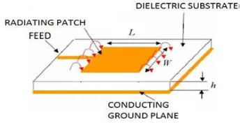
Structure of micro strip patch antenna consists of radiating patch on top side, ground plane on bottom side, dielectric substrate in between the patch and ground plane. The radiating patch can be any possible shape. Although the trends are for rectangular patches, other conductor shapes have similar responses.
Fig. 4.1 Microstrip patch antenna[7]
ISSN(Online): 2320-9801
ISSN (Print): 2320-9798
International Journal of Innovative Research in Computer
and Communication Engineering
(An ISO 3297: 2007 Certified Organization)
Vol. 3, Issue 6, June 2015
second most common shape. These patches are slightly smaller than their rectangular counterpart and as a result have slightly lower gain and bandwidth. Different shapes of patch are shown in below figure
Fig. 4.2 Representative shapes of microstrip patch elements[7]
4.2 Advantages and Disadvantages of Microstrip Antennas
Advantages :
Microstrip antennas have several advantages compared to conventional microwave Antennas, include
(1) Planar, which can also be made conformal to a shaped surface (2) Low profile
(3) Low radar cross-section (4) Rugged
(5) Can be produced by printed circuit technology (6) Can be integrated with circuit elements
(7) Can be designed for dual polarization operations (8) Can be designed for dual or multi-frequency operations
These advantages make microstrip patch antennas much more suitable for aircrafts, spacecrafts, and missiles than conventional antennas as they do not interfere with the aerodynamics of these moving vehicles
Disadvantages
The microstrip antennas also have some disadvantages compared to conventional Microwave antennas including
(1) narrow bandwidth (2) lower gain due to loss
(3) lower power handling capability
(4) possibility of excitation of surface waves
4.3 Feeding Techniques:
The microstrip antenna may be fed in various ways. These methods can be classified into two categories – contacting and non-contacting. The four most popular feed techniques used are the microstrip line, coaxial probe, aperture coupling and proximity coupling. [1]
4.3.1 Coaxial probe feed
ISSN(Online): 2320-9801
ISSN (Print): 2320-9798
International Journal of Innovative Research in Computer
and Communication Engineering
(An ISO 3297: 2007 Certified Organization)
Vol. 3, Issue 6, June 2015
is soldered to the patch metallization. The location of the feed point is determined for the given mode so that the best impedance match is achieved. Excitation of the patch occurs principally through the coupling of the feed current Jz to the Ez field of the patch mode.
Fig. 2.4 Four common feeding methods of microstrip patch antenna[8]
4.3.2 Microstrip (coplanar) Feeds
Excitation of the microstrip antenna by a microstrip line on the same substrate appears to be a natural choice because the patch can be considered an extension of the microstrip line, and both can be fabricated simultaneously. but this technique has some limitations. The coupling between the microstrip line and the patch could be in the form of edge/butt- in coupling or through a gap between them.
4.3.3 Proximity (Electromagnetically) Coupled Microstrip Feed
A configuration of this non-contacting, non-coplanar microstrip feed is shown in figure. It uses a two-layer substrate with the microstrip line on the upper layer. The feed line terminates in an open end underneath the patch. This feed is better known as an “electromagnetically coupled” microstrip feed. Coupling between the patch and the microstrip is capacitive in nature. The open end of the microstrip line can be terminated in a stub and stub parameters can be used to improve bandwidth. Bandwidths of the order of 13% have been achieved using this feed.
The substrate parameters of the two layers can be selected to increase the bandwidth of the patch and to reduce spurious radiation from the open end of the microstrip for this, the lower layer should be thin. The radiating patch being placed on the double layer gives a larger bandwidth. Fabrication of this feed is, however, slightly more difficult because of the requirement for accurate alignment between the patch and the feed line, but soldering is eliminated.
4.3.4 Aperture- coupled microstrip feed
ISSN(Online): 2320-9801
ISSN (Print): 2320-9798
International Journal of Innovative Research in Computer
and Communication Engineering
(An ISO 3297: 2007 Certified Organization)
Vol. 3, Issue 6, June 2015
V. DESIGNCONSIDIRATIONANDSIMULATIONRESULTSUSINGROGERSTMM3
5.1 Steps to Design a rectangular Microstrip Patch Antenna
(1) Choose a substrate material. i.e. FR4 Epoxy with Ɛr = 4
(2) Decide a frequency range and resonant frequency where you want to make your antenna resonate. i.e. fr= 3.5 GHz within S-band (2 to 4 GHz)
(3) Select height of a substrate (h) and a patch material (t). They are always h ≤ 0.05 λ0 and t≤ λ0 (4) Calculate widths and lengths of patch and ground plane.
(5) Decide a feeding technique which is well suited for your design. I.e. Coaxial feed or microstrip line feed which are most commonly used.
(6) Find size of inner and outer and its location in case of coaxial feed and dimensions of microstrip line and its location in case of microstrip line feed for impedance matching.
(7) Design an antenna using any simulation software like CST microwave studio, HFSS or IE3D using all above values.
(8) Observe simulated return loss by varying the feed location until you get desired return loss (i.e.S11 = -40dB) at the resonant frequency.
(9)Then observe other simulation results such as gain, directivity, smith chart, vswr, etc.
5.2
Coaxially fed Rectangular Microstrip Patch Antenna Design
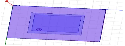
Fig5.1 Coaxial fed microstrip patch antenna design
5.2.1 Simulation Results
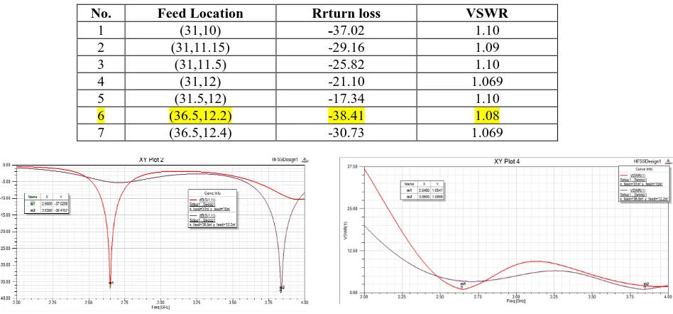
Table. 1 Effects of Feed Location on Return Loss and VSWR
No. Feed Location Rrturn loss VSWR
1 (31,10) -37.02 1.10
2 (31,11.15) -29.16 1.09
3 (31,11.5) -25.82 1.10
4 (31,12) -21.10 1.069
5 (31.5,12) -17.34 1.10
6 (36.5,12.2) -38.41 1.08
7 (36.5,12.4) -30.73 1.069
ISSN(Online): 2320-9801
ISSN (Print): 2320-9798
International Journal of Innovative Research in Computer
and Communication Engineering
(An ISO 3297: 2007 Certified Organization)
Vol. 3, Issue 6, June 2015
5.3 Coaxially fed Microstrip stacked Patch Antenna design
5.3.1 Introduction of stacked patch
Vertical slot loaded upper patch
Horizontal slot loaded lower fed patch
h
1h
2Coaxial Probe feed
Fig. 5.4 stacked patch antenna [3]
Figure show the side view of stacked patch microstrip patch antenna which is coaxially fed. Stacked patch antenna is kind of microstrip which consists of two printed antenna. The lower patch is called driven patch and another patch is parasitically coupled to driven patch. To produce broadband responses the selection of the substrate of the first layer is very important. The current distribution on the lower patch has an important role on the bandwidth of the antenna. If the lower dielectric layer has a greater dielectric constant than the upper layer, the magnitude of the first order mode on the lower patch will be greater than on the top patch thus the broadest bandwidths can be achieved.
The thickness of each layer has an important role to obtain broader bandwidth. In the design process the lower patch does not design for minimum return loss in the desired band, rather than the patch should be strongly capacitive over this frequency range. To provide this, feed position of the antenna become near the edge of the patch
Fig 5.5 coaxially fed stacked patch microstrip antenna design using FR4 epoxy material
5.3.2 Simulation Results
Table 2. Effects of Feed Location on Return Loss and VSWR
No. Feed Location Rrturn loss VSWR
1 (15,9) -18.92 1.2
2 (38,9) -20.95 1.19
3 (15,10) -30.39 1.06
4 (16,10) -46.17 1.06
5 (17,10) -21.04 1.19
6 (17,11) -44.72 1.01
Substrate-2
ISSN(Online): 2320-9801
ISSN (Print): 2320-9798
International Journal of Innovative Research in Computer
and Communication Engineering
(An ISO 3297: 2007 Certified Organization)
Vol. 3, Issue 6, June 2015
Fig 5.6 Return loss for feed location (16, 10) Fig 5.7 VSWR for feed location at (16, 10)
5.4 Coaxially fed Double U – slot stacked patch microstrip antenna design
Two U- slots are cut on the upper patch of the stacked patch microstrip antenna which is coaxially fed. U slot behaves as a serial capacitor thus the inductive behaviour of probe feed can be compensated and impedance matching can be optained. The main advantages of U-slot patch antenna is that it produces broad band characteristics with a single and simple topology. The variations of U-slot patch antenna paramaters such as slot widht, slot lenght, height and size of the patch, probe location and substrate permitivity can dramatically change the antenna’s behaviour. Analytical procedures have not been develop to design U-slot patch antenna. Dimensional invariance and resonance frequency approaches are well known empirical design procedures in literature. These approaches are useful for initial designs and desired antenna behaviour can be obtained after some optimizing and tuning process
To improve return loss more than we got in stacked patch microstrip patch antenna, we design double U- slot stacked patch microstrip antenna which is coaxially fed. Fig. 4.14 shows the design of coaxial fed Double U- slot stacked patch microstrip antenna. Geometry of this antenna is same as stacked patch microstrip antenna. Just two U- slot are cut on the upper patch of antenna.
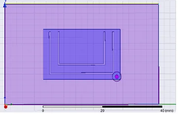
Fig 5.8 coaxial fed Double U- slot stacked patch microstrip antenna design
5.4.1 Simulation Results
Table 3. Effects of Variation in Length of Inner U-Slot on Return Loss and VSWR
Sr.No Variation in length (li mm) of inner U -slot
Return Loss (S11) in dB VSWR
1 3 -35.44 1.008
2 4 -49.16 1.007
ISSN(Online): 2320-9801
ISSN (Print): 2320-9798
International Journal of Innovative Research in Computer
and Communication Engineering
(An ISO 3297: 2007 Certified Organization)
Vol. 3, Issue 6, June 2015
Table 4. Effects of Variation in Width ws of Inner U-Slot on Return Loss
Fig 5.9 return loss for length of inner U- slotLi=4mm Fig 5.10 VSWR for length of inner U- slot Li = 4mm
VI. CONCLUSION
By this research work, the return loss reduction can be achieved using double U – slot stacked patch technique using FR4 epoxy material in microstrip patch antenna which is fed by coaxial probe. the best return loss i.e. RL = -49.16 dB at resonate frequency Fr = 3.53dB is achieved by this design technique. The microstrip patch antenna designed and simulation is being done using HFSS at resonant frequency 3.5GHz
.
.
REFERENCES
[1] Hemant Kumar VarshneyȦ*, Mukesh KumarȦ, A.K.JaiswalȦ, Rohini SaxenaȦ and Komal JaiswalȦ “ A Survey on Different Feeding Techniques of Rectangular Microstrip Patch Antenna” , Published in International Journal of Current Engineering and Technology Accepted 02 May 2014, Available online 01 June 2014, Vol.4, No.3 (June 2014)
[2] Mrs.Hetal .M. Pathak , Chaudhary pankaj prabhubhai “Stacked Modified Patch Antenna Comparison for Various Dielectric Material” published in Machine Intelligence Research and Advancement, 2013 International Conference.
[3] Siddiqui Naushad Ather1, Rajesh Kumar verma2, P.K. Singhal3, “Bandwidth Enhancement for Truncated Rectangular Microstrip Antenna Using Stacked Patches and Defected Ground Structure” published in Computational Intelligence and Communication Networks, 2013 5th International Conference.
[4] Naresh Kumar Joshi, Manisha Uttamrao Birare, Neeraj Nahata “Design of Microstrip Stacked Square Patch Antenna” Published in International Journal of Engineering and Innovative Technology (IJEIT) Volume 2, Issue 3, September 2012
[5] D.K. Srivastava1*, J.P. Saini1, D.S. Chauhan2 “Wideband electromagnetically coupled coaxial probe fed slot loaded stacked patch antenna” Published in International Journal of Engineering, Science and Technology Vol. 3, No. 3, 2011, pp. 154-159
[6] Lee Chia Ping1, Chandan Kumar Chakrabarty2 & Rozanah Amir Khan3,” Design of Ultra Wideband Slotted Microstrip Patch Antenna” Proceedings of the 2009 IEEE 9th Malaysia International Conference on Communications 15 -17 December 2009 Kuala Lumpur Malaysia [7] Balanis, Constantine A. Antenna theory: analysis and design. John Wiley & Sons, 2012.
[8] Lee, Kai Fong, and Kwai Man Luk. Microstrip patch antennas. Vol. 1. London: Imperial College Press, 2011.
Sr.No
Variation in width (ws mm) of inner U -slot
Return Loss (S11) in dB
Freq
1 21 -38.14 3.53
2 22 -49.16 3.53
![Fig. 4.2 Representative shapes of microstrip patch elements [7]](https://thumb-us.123doks.com/thumbv2/123dok_us/1483649.1181518/3.595.208.392.202.308/fig-representative-shapes-microstrip-patch-elements.webp)
![Fig. 2.4 Four common feeding methods of microstrip patch antenna [8]](https://thumb-us.123doks.com/thumbv2/123dok_us/1483649.1181518/4.595.156.444.235.360/fig-common-feeding-methods-microstrip-patch-antenna.webp)