Ultra-Low-Power FRAM-based MCUs
Amir Moradi and Gesine Hinterw¨alder
Horst G¨ortz Institute for IT-Security, Ruhr-Universit¨at Bochum, Germany {amir.moradi, gesine.hinterwaelder}@rub.de
Abstract. By shrinking the technology and reducing the energy require-ments of integrated circuits, producing ultra-low-power devices has prac-tically become possible. Texas Instruments as a pioneer in developing FRAM-based products announced a couple of different microcontroller (MCU) families based on the low-power and fast Ferroelectric RAM tech-nology. Such MCUs come with embedded cryptographic module(s) as well as the assertion that – due to the underlying ultra-low-power tech-nology – mounting successful side-channel analysis (SCA) attacks has become very difficult. In this work we practically evaluate this claimed hardness by means of state-of-the-art power analysis attacks. The leak-age sources and corresponding attacks are presented in order to give an overview on the potential risks of making use of such platforms in security-related applications. In short, we partially confirm the given as-sertion. Some modules, e.g., the embedded cryptographic accelerator, can still be attacked but with slightly immoderate effort. On the contrary, the other leakage sources are easily exploitable leading to straightforward attacks being able to recover the secrets.
1
Introduction
Side-Channel Analysis (SCA) attacks have become a serious threat to tographic implementations. Regardless of the theoretical robustness of a cryp-tographic primitive, secret materials used by its implementation can easily be recovered in case of absence of SCA-dedicated countermeasures. Case studies like [1, 4, 11–13] confirmed the effectiveness of such attacks to overcome the se-curity of commercial products. Hence, the producers of sese-curity-related appli-cations have moved towards integrating SCA countermeasures. For example the FPGA architectureUltraScale[18] – recently announced by Xilinx – offers many security features including DPA-protected bitstream encryption. Along the same lines, Microsemi has integrated many solutions to improve physical security of Actel’s FPGA familySmartFusion2 [10].
power consumption compared to equivalent flash memories. The low power con-sumption as well as the embedded cryptographic modules (e.g., an AES core) are the key factors of the offered security. It is claimed that due to the ultra-low-power feature of such MCUs and their low operating voltage (1.5 V) SCA attacks become extremely difficult to mount.
This article deals with the aforementioned features and presents practical investigation results with respect to the claimed hardnesses. The results of our analyses on an MSP430FR5969 MCU are summarized as:
– A couple of different power analysis attacks are feasible on the embedded AES module. We should highlight that such attacks are not as straight-forward as those mounted on crypto engines of other MCUs e.g., Atmel’s XMEGA [8]. That difference is mainly due to the low-power feature of the integrated AES module.
– Regardless of the underlying low-power architecture, software implementa-tions of cryptographic algorithms executed on the underlying MCU are vic-tims of power analysis attacks. Unsurprisingly, the secrets of such implemen-tations can be easily revealed by means of straightforward state-of-the-art attacks.
– Due to the restricted speed of the FRAM technology, TI integrated a dedi-cated cache to be used when the MCU operates at a higher frequency than the access frequency of FRAM. As a known issue, the cache (miss/hit) can be a source of SCA leakage. We report case studies, which make use of this feature to launch effective SCA attacks.
– The internal architecture of MCUs is usually not known to end users. Such architectures can turn an implementation of a sound masking scheme to a vulnerable design. In order to examine such issues we consider an imple-mentation of themasking with randomized look-up tablecountermeasure [14] which has particularly been developed for FRAM-based MCUs [7]. Our anal-ysis shows that the unknown internal architecture of the underlying MCU causes the provably-secure masked design to have a first-order leakage, while it is supposed to provide security at all orders.
2
Features
Here we shortly recall a couple of features of TI’s FRAM-based MCUs. We focus on those specifications, which are related to our security analyses.
2.1 AES Accelerator
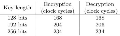
Table 1.AES accelerator performance figures
Key length Encryption Decryption (clock cycles) (clock cycles)
128 bits 168 168
192 bits 204 206
256 bits 234 234
that the AES module has not been designed for speed-critical applications al-though it can perform a complete encryption and decryption much faster than corresponding software on the same MCU. Table 1 shows the number of clock cycles the AES module requires to complete the respective operations.
As it is a stand-alone module, the MCU can perform other operations while the AES module is busy. It is noteworthy that the numbers given in this table are with respect to the on-the-fly computation of round keys while the decryption module requires to receive the last round key. The interested reader is referred to [17] for more detailed information including the performance of the other modes.
2.2 FRAM Architecture
As a promising alternative to non-volatile storage such as flash, FRAM technol-ogy offers many advantages. It avoids the long delays as well as the high current supply required for programming (writing). The advantageous features of the FRAM technology focus mainly on write operations. High speed (125 ns delay), low power (82µA/MHz), and super high (1015) write cycles have been reported for the 130 nm MSP430FR family of TI’s MCUs.
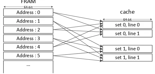
As a disadvantage we should refer to the fact that FRAM reads are destruc-tive. That is, every read must be followed by a write operation (with the same data). However, this is automatically handled by the FRAM controller, and the end user does not need to pay any attention to this. Therefore, the frequency of FRAM read operations are limited to the write speed. Due to this limit, TI has integrated a read cache in front of the FRAM to accelerate the operations in case the MCU operates at a higher frequency than the FRAM. In the MSP430FR family, the FRAM can be operated at up to 8 MHz without use of this cache. When the MCU operates at a frequency of 16 MHz (the maximum operation frequency of the MSP430FR family), the cache is utilized.
set 0, line 0 set 0, line 1
set 1, line 0 set 1, line 1 Address : 0
Address : 1 Address : 2 Address : 3 Address : 4 Address : 5
... 64-bit
64-bit FRAM
cache
Fig. 1.Structure of the two-way associative cache
FRAM access. Therefore, memory read accesses on consecutive addresses can be executed without wait states when they are within the same cache line.
Each 64-bit location in FRAM can be cached in only one of the two sets in the cache. As shown in Figure 1, the most common scheme is to use the least significant bit of the FRAM location’s address as the indicator to the corre-sponding cache set. We should emphasize that FRAM contains both program code and data, e.g., look-up tables, which are to be stored in the non-volatile memory. Hence, frequent jumps and frequent accesses to the pre-stored tables in FRAM can negatively affect the cache performance.
3
Analyses
In this section we present various analyses that we performed on an FRAM-based MCU. We first present the framework that we used, and then describe each analysis in detail.
3.1 Setup
The practical analyses have been conducted on an MSP-EXP430FR5969 Launch-pad Evaluation Kit, and we used IAR Embedded Workbench IDE as well as Code Composer Studio to develop and compile the codes. This evaluation platform has been developed to facilitate power measurements. As shown in Figure 2, we could easily place a 1.8 Ω resistor at the VCC path of the MSP430FR5969 MCU while no stabilizing capacitor was placed between the measurement point and the MCU. We monitored the current passing through the MCU by means of a LeCroy WaveRunner HRO 66Zi digital oscilloscope at a sampling rate of 1 GS/s. We also used an I/O pin of the MSP-EXP430FR5969 Launchpad Evaluation Kit as trigger signal to align the collected traces. We provided a 16 MHz crystal oscillator as external clock source, and by clock source configurations drove the MCU at our desired frequency (explained below for each target).
X430 FR5969
VCC
1.8 Ω
DC Mode 50 Ω DC blocker
Vdd
Amp.
Fig. 2.Measurement setup
from Mini-Circuits) to collect the power traces with a considerably high quality. Further, we limited the oscilloscope bandwidth to 20 MHz to reduce the electrical noise.
Metrics: For the side-channel analysis we mainly used correlation power analy-sis (CPA) [3] to mount key-recovery attacks. However, in some cases we applied a statisticalt-test [5]. The goal of such a scheme is not to examine a key-recovery attack, but rather it provides an overview of the existence of a leakage which might be exploited by an attack. The concept oft-test is based on the classical DPA attack of [9].
Following the concept of DPA, the traces t ∈ T are categorized into two groupsg1andg2. Recall that Welch’s (two-tailed) t-test is computed as
t= µq(t∈g1)−µ(t∈g2)
δ2(t∈g 1)
|g1| +
δ2(t∈g 2)
|g2|
,
where µ andδ2 denote the sample mean and the sample variance respectively, and|.|stands for the cardinality. Thet-test indeed examines the validity of the null hypothesis as the samples in both groups (g1 andg2) were drawn from the same population. If the null hypothesis is correct, it can be concluded with a high level of confidence that a corresponding DPA attack cannot exploit the leakage.
For such a conclusion the Student’st-distribution density function in addition to the degree of freedom is applied to determine the probability of rejecting the aforementioned hypothesis (for more information see [5]). For typical evaluations, a threshold for|t|as>4.5 is defined to reject the null hypothesis and conclude that the device exhibits a first-order leakage. This process is repeated at each sample point independently.
output bit directs the classification. Many intermediate values should be con-sidered in the evaluations to examine the feasibility of each corresponding DPA attack. Instead, a non-specific t-test can be performed, which can examine the existence of leakage without any required intermediate value. In such a test, a fixed input (plaintext) is selected, and the measurements are randomly inter-leaved between the fixed and random inputs. So the non-specific t-test is also calledfixed vs. randomt-test. Hence, based on the given input (fixed or random) the traces are categorized into g1 and g2. It is noteworthy that such a leakage assessment scheme has been also used in [2].
3.2 AES Hardware Accelerator
As the first target we focus on the AES accelerator. As stated in Section 2.1, the AES module can perform the encryption and decryption functions in a couple of different settings. We evaluate only the AES-128 encryption function with on-the-fly round key computation, which takes 168 clock cycles. Following the con-figurations given in [17] we developed assembly code (in IAR Embedded Work-bench IDE) to activate the aforementioned function. We intentionally wrote the code in such a way that it waits in a loop till the operation of the requested encryption is finished. It allows us to observe only the leakage of the AES ac-celerator module. Further, we configured the MCU to operate at a frequency of 2 MHz.
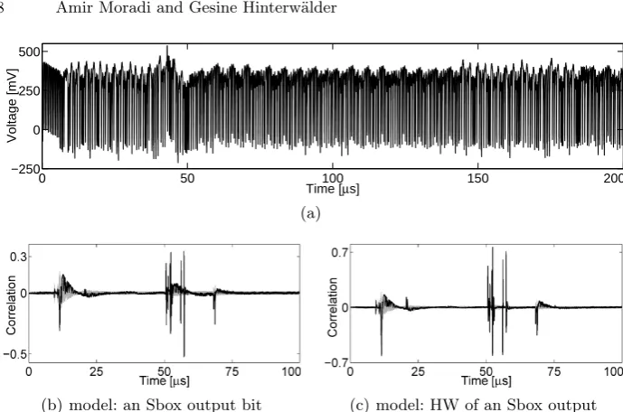
Figure 3(a) shows an exemplary power trace confirming its ultra-low power consumption. In order to examine the vulnerability of such a module to power analysis attacks, we first performed a couple of specifict-tests with intermediate values including i) the cipher round output bits (128 cases), ii) XOR between the cipher input and output bits (128 cases), iii) the SubBytes output bits (128 cases), iv) XOR between the SubBytes input and output bits (128 cases), v) the SubBytes output bytes (16×256 cases), and vi) XOR between different Sbox output bits ( 162
×8 cases). The best results have been achieved considering the SubBytes output bits as well as the XOR between the SubBytes input and output bits (cases iii and iv). As a proof of concept we performed CPA attacks with the corresponding power models. For instance, Figure 3 presents the results of two CPA attacks using 100 000 traces. The power models have been chosen as i) an Sbox output bit and ii) a bit of the XOR result of an Sbox input and output. It is noteworthy that the attacks with common power models like Hamming weight (HW) models are also feasible, but not as efficient as those mentioned above.
0 20 40 60 80 −40
0 40 80
Time [μs]
Voltage [mV]
(a)
(b) model: an Sbox output bit (c) model: a bit of Sbox input XOR output
Fig. 3.AES in hardware: (a) a sample trace (full AES), (b) and (c) CPA attack results using 100 000 traces
been stored in FRAM. In short, when the MCU operates simultaneously with the AES accelerator, the above-presented attacks become harder.
3.3 AES in Software
As a case study to examine the leakage of the normal operation of the MCU, we took the AES-128 implementation recommended by TI and publicly available at
http://www.ti.com/tool/AES-128. Both encryption and decryption functions are written in C, and we used IAR Embedded Workbench IDE to compile the encryptioncode and ran it on our evaluation kit at a frequency of 8 MHz. We first realized that the length of the traces is not constant, and the implementation needs different number of clock cycles depending on the plaintext. The source of this issue was found in the way that multiply by 2 (used for MixColumns) has been implemented:
1 u n s i g n e d c h a r g a l o i s _ m u l 2(u n s i g n e d c h a r v a l u e) {
3 if (value> >7) {
5 r e t u r n ((v a l u e < < 1) ^0x1b) ; } e l s e
0 50 100 150 200 −250
0 250 500
Voltage [mV]
Time [μs]
(a)
(b) model: an Sbox output bit (c) model: HW of an Sbox output
Fig. 4.AES in software @ 8 MHz: (a) a sample trace (first round), (b) and (c) CPA attack results using 100 000 traces
As a result the implementation is vulnerable to a classical timing attack by predicting whether the extra reduction (XOR by the polynomial) is required or not. We have implemented such an attack and could easily recover the key using less than 5000 timing measurements (of the full encryption). Further, such an implementation is trivially vulnerable to a simple power analysis attack, where by observing each power trace the adversary can conclude whether the extra reduction was performed or not directly leading to a shrink in the key space.
Regardless of this issue we examined the efficiency of the start-of-the-art power analysis attacks. A sample trace covering the first round of the encryption is shown in Figure 4(a). In short, several attacks by different hypothetical power models are feasible, as expected. The results of two CPA attacks predicting a bit of an Sbox output as well as the HW of the Sbox output are shown in Figure 4. It is noteworthy that compared to the AES accelerator, the leakages associated with the execution of the MCU instructions are an order of magnitude easier to exploit. In fact, the ultra-low-power feature of the underlying MCU does not play an important role to harden the attacks.
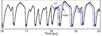
3.4 Cache
16 17 18 19 20 Time [μs]
miss
hit
Fig. 5.AES in software @ 16 MHz: detection of cache miss/hit through power traces
a frequency of 16 MHz. Figure 5 shows a couple of traces during the SubBytes operation (one Sbox call). It can be seen that the traces belonging to cache hit and cache miss are clearly distinguishable. Therefore, a trace-driven cache attack is possible. In other words, by comparing a couple of traces the attacker would be able to detect whether each Sbox call caused a cache miss or not.
For an attack scenario let us consider two consecutive Sbox callsS(p1⊕k1) and S(p2⊕k2). If by observing the power traces the attacker detects a cache hit during the second Sbox call, it can be directly concluded that the two Sbox calls accessed nearby memory locations. Therefore, the attacker can gain certain information about ∆k = k1⊕k2 = p1⊕p2. With respect to the underlying cache architecture, i.e., 64-bit lines (8 bytes), the five most significant bits of ∆k can be recovered by the attacker. This is true, if the Sbox table starts at a location in FRAM corresponding to the first byte of a cache line. In other words, the first entry of the Sbox table needs to be stored in a location with address
xx...xx000. Otherwise, the recovered bits of ∆k is reduced to the four most significant bits.
As a proof of concept we developed a scenario to perform such an attack. In such a scenario we collected 256 power traces Ti∈{0,...,255} where the first plaintext byte p1 is constantly set to an arbitrary value, e.g., 0, and the second one p2 = i. The rest of the plaintext bytes can be arbitrarily selected. By observing the power traces and detecting a cache hit with p2 = p0
2, a part of k1⊕k2 = p0
2 is recovered. Indeed, it is not required to collect all 256 traces; once a cache hit is detected the process can be terminated. For the second phase of the attack, again at most 256 traces are collected with plaintext bytesp1= 0, p2 = p0
2, and p3 = i. The same process is repeated to find the colliding case for p3 =p0
3 and recovering a part of k1⊕k3 = p03. The selection of p2=p02 is necessary to avoid replacing the part of the cache filled during the first Sbox call. This process is repeated for the other plaintext bytes. At the end of the attack, the key space is limited to 25·23×16= 253 or to 24·24×16= 268 depending on the location the Sbox table is stored in. However, the attack can be extended to the second round and recover more relations to again shrink the key space.
10 Amir Moradi and Gesine Hinterw¨alder
x
m
k
C
S
S
(
x
⊕k
)
⊕S
(
x
⊕m
⊕k
)
S
(
x
⊕m
⊕k
)
x
m
RC
R
G
1
S
(
x
⊕m
⊕a
1⊕k
)
⊕a
2S
(
x
⊕k
)
⊕a
3S
(
x
⊕m
⊕a
1⊕k
)
⊕a
2(a)
x
m
C
S
S(x⊕k) ⊕
S(x⊕m⊕k)
S(x⊕m⊕k)
x
m
RC
R
g
1 S(x⊕m⊕a1⊕k)⊕a2S(x⊕k) ⊕a3⊕
S(x⊕m⊕a1⊕k)⊕a2 (b)
Fig. 6.(a) classical Boolean masking, (b) the scheme of [7]
case, the instructions performed between two consecutive Sbox calls can already replace the interesting line of the cache and avoid any cache hit by the second call. The presented attack scenario is only an example of a common scheme in the presence of a cache. It should also be emphasized that since the cache is shared between the program and data memory, exploiting the leakage by timing attacks (as a time-driven cache attack) is not trivial. In general, we show the leakage sources which should be taken into account when using such an MCU in a security-related application.
3.5 Internal Architecture
As the last case study we considered a masking scheme, which has been developed to provide security against side-channel attacks at any order. The scheme, which is based on the work presented in [14] has been implemented on an FRAM-based MCU as a proof of concept [7]. Therefore, we could easily integrate the same program code on our platform and perform the evaluations.
With respect to Figure 6, we restate the underlying scheme. In a classical first-order Boolean masking (Figure 6(a)), x and m (resp. input and random mask) are given to the device, which generates two outputs as S(x⊕m⊕k) andq:S(x⊕m⊕k)⊕S(x⊕k) as a shared representation ofS(x⊕k). Such a scheme is certainly vulnerable to a second-order attack combining the leakages associated with the output shares. The concept followed in [14] and [7] is to involve more random data in the computations in such a way that the look-up tables g1, R, and RC are precomputed based on the predefined key k and random dataa1, a2, and a3 in a secure environment (see Figure 6(b)). During the operation (similar to the classical Boolean masking) xand m are given to the device, and all the operations are performed by the aforementioned look-up tables. As each of the look-up tables involves a randomai which is independent
of the others, the adversary should not be able to recover any information by combining the leakage of the look-up tables and/or the output shares.
Algorithm 1: Look-up Table Precomputation input :k,a1,a2, anda3
output:g1(·,·),R(·),RC(·,·), andg2(·,·)
∀i, j;g1(i, j) = i⊕j⊕a1
∀i; R(i) = S(i⊕k)⊕a2
∀i, j;RC(i, j) =S(i⊕k)⊕a2⊕S(i⊕j⊕k⊕a1)⊕a3
∀i, j;g2(i, j) = i⊕j⊕a3
Algorithm 2: Operation
input :x,m,g1(·,·),R(·), andRC(·,·)
output: (s1, s2)
g= g1(x, m) ;/* :x⊕m⊕a1 */
s1=R(g) ;/* :S(x⊕m⊕a1⊕k)⊕a2 */ s2=RC(g, m) ;/* :S(x⊕m⊕a1⊕k)⊕a2⊕S(x⊕k)⊕a3 */
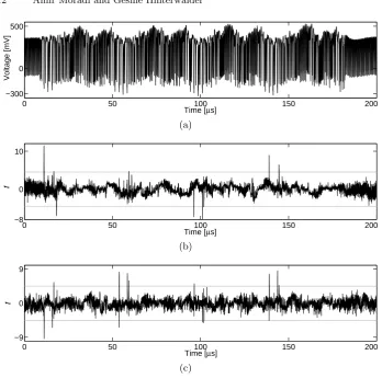
A simplified and reduced version of the LED cipher [6] has been considered in [7] as an example to be implemented by the above-restated scheme. This reduced LED consists of only four rounds (cf. Figure 7) and a 16-bit (4×4) data width (i.e., it works only on the first column of the full LED state). We integrated the corresponding code and ran the MCU at a frequency of 8 MHz. It should be noted that before each encryption the look-up tablesg1,g2,R, and RC are recomputed, i.e., there is no mask reuse in the whole scheme. By means of appropriate trigger signals as well as inserting a large enough gap between the precomputation phase and the operational phase we made sure to measure the power consumption of the MCU only during the operational phase. As we planned to perform anon-specifict-test, we collected 150 000 traces while a fixed value (as 0) or a random one – in a randomly interleaved fashion – was given to the MCU as plaintext. The result of both first- and second-order univariate t-tests are shown in Figure 8. Unexpectedly, the tests report both first- and second-order leakages.
Fig. 6.Reduced version of the block cipher LED.
While such a cipher is naturally too small for being deployed in actual ap-plications, we use it to refine our model for RLUT performance estimates. As will be discussed in the next sections, scaling to larger number of rounds and block size (e.g. the full 64-bit LED cipher) will be possible in soon available 128-and 256-kilobyte versions of our FRAM microcontroller. In the figure, the 4-bit S-boxes of LED are denoted asS, and its linear diffusion layer asMixColumns.
4.3 Implementation in FRAM microcontrollers
We now describe how to implement reduced (with up to 4 rounds) LED ciphers within the 16 kilobytes of FRAM available in our MSP430FR microcontroller.
The first building block required in a RLUT-masked implementation is a randomness generator (needed to produce the ai values of Algorithm 1). For illustration, we used a LFSR with CRC-32 polynomial for this purpose (al-ternative ways of generating randomness could of be considered, e.g. using a leakage-resilient PRG if leaking pre-computations are considered [5, 17]).
Next, the part computing the randomized program can be implemented quite straightforwardly, following the description in Section 4.1. The trickiest bit was to efficiently arrange 4-bit outputs into memory bytes, without giving any un-necessary information on the RLUT input values3. Using one byte to store two consecutive RLUT outputs was rejected, since accessing one or the other value in the byte would have led to different code behaviors, depending on the LSB bit of the RLUT’s input. Instead, we stored the outputs coming from two different RLUTs for the same input value in a single byte. This time, the LSB (resp. MSB) part of one byte will be accessed when an odd (resp. even) word of the state needs to be computed, giving no information on the word’s value itself. Based on this strategy, the RLUTsR andRC can be generated efficiently from the cipher key, the S-Box and the table map, that are all stored in memory.
3This has no impact on the security in case of secure pre-computation, but may
increase the information leakage in case of online randomization of the tables.
0 50 100 150 200 −300
0 500
Voltage [mV]
Time [μs] (a)
0 50 100 150 200
−8 0 10
t
Time [μs] (b)
0 50 100 150 200
−9 0 9
t
Time [μs] (c)
Fig. 8.Reduced LED @ 8 MHz: (a) sample trace (operational phase), (b) and (c)t-test results first- and second-order respectively using 150 000 traces
As stated, the scheme is supposed to provide resistance against the attacks at any order. The exploitable leakage, that we presented, is not due to the under-lying scheme. In other words, we do not report any flaws in the algorithm or in the implementation of [7]. Instead, we show that even theoretically-sound cotermeasures can fall into failure because of the internal architecture of the un-derlying platform. By slightly changing the program code and performing many measurements and analyses, we found out that the instructions which perform the table look-ups are the source of the observed leakages. More precisely, the exemplary instruction
1 mov.b @pointer, m0
pinpointed. Further, although we showed an exploitable leakage, the evaluation we performed (non-specifict-test) cannot give a clear assessment on the hardness of an attack exploiting such leakage.
We give an example to show the strong effect of the MCU’s internal archi-tecture on the side-channel vulnerability. We observed that if a random value is written to a location in FRAM the leakage associated with this write operation depends on the value which has been previously stored in that location. In other words, suppose that xhas been stored at location address. A write operation,
which stores a random value m at locationaddress, leads to a leakage associ-ated with the value ofxas well. We observed such leakage during the evaluation of the above-expressed reduced LED implementation. At one point in the code (during the operational phase) a masked intermediate value is stored at a loca-tion where the unmasked plaintext had been stored before (at lines 4 and 7 of the below code):
1 mov #STATE, p o i n t e r
r l a m #4 , st0
3 add st1, st0
mov.b st0, 0(p o i n t e r)
5 r l a m #4 , st2
add st3, st2
7 mov.b st2, 1(p o i n t e r)
In order to avoid such a strong leakage (shown in Figure 9) we cleared the contents of this location during the precomputation phase by:
1 mov #STATE, p o i n t e r
mov.b #0x00,0(p o i n t e r)
3 mov.b #0x00,1(p o i n t e r)
This indeed is an evidence to the statement given above. We believe that such leakage is due to the FRAM architecture as well as the way a write operation is performed.
0 50 100 150 200
−25 0 60
t
Time [μs]
4
Conclusions
In this work we have extensively examined the side-channel vulnerability of FRAM-based MCUs of Texas Instruments as a platform for cryptographic ap-plications. The motivation of this work is related to the relevant announcements dealing with the ultra-low-power feature of such MCUs and the claims on the hardness of power analysis attacks. Hence, we focused only on the power con-sumption of the underlying device and presented the corresponding evaluation results. The covered targets include the embedded AES accelerator (hardware), ordinary instructions of the MCU (software), FRAM cache, and the MCU inter-nal architecture. In short, by means of practical investigations we confirm the hardness (but still feasibility) of the attacks on the embedded AES accelerator compared to similar targets of such attacks, e.g., the embedded AES core of At-mel’s XMEGA MCUs. Such a hardness is mainly due to its low-power technology which leads to a high noise level in the measurements. However, when a cryp-tographic algorithm is implemented by the general-purpose MCU instructions, our practical results showed feasibility of straightforward and common DPA at-tacks without any serious difficulties. The cache, which has been integrated to accelerate the FRAM accesses, also comes with known security issues. Since an FRAM read must be followed by an FRAM write with the same value due to its destructive nature, an FRAM access consumes much more energy compared to a cache access. Hence, cache hit/miss can be clearly distinguished by observ-ing the power traces. Although the cache is shared between the program and data memory (in MSP430FR5xxx family), we have shown that the trace-driven cache attacks (which exploit the sequence of cache misses/hits) are expectedly feasible. We also took a masking scheme into account, that has been developed in particular for platforms with a large non-volatile memory, e.g., FRAM-based MCUs. The scheme is based on precomputed randomized look-up tables and is expected to provide security against side-channel attacks of any order. Although there are no theoretical flaws in its developments, we have demonstrated that its implementation cannot pass a general leakage assessment test. The reason for such a failure lies in the details of the implementation platform (the MCU) regardless of the soundness of the underlying masking scheme.
On the one hand, the results we presented here are more or less expected as we targeted an unprotected platform where side-channel analysis should be feasible. On the other hand, this work gives an overview about the feasibility of exploiting various leakage sources of the underlying platform. Such informa-tion spreads awareness of the available leakage sources, and is certainly useful for cryptographic engineers, who deal with such a platform for security-related applications.
Acknowledgment
References
1. J. Balasch, B. Gierlichs, R. Verdult, L. Batina, and I. Verbauwhede. Power Analysis of Atmel CryptoMemory - Recovering Keys from Secure EEPROMs. InCT-RSA 2012, volume 7178 ofLNCS, pages 19–34. Springer, 2012.
2. B. Bilgin, B. Gierlichs, S. Nikova, V. Nikov, and V. Rijmen. Higher-Order Thresh-old Implementations. InASIACRYPT 2014, volume 8874 ofLNCS, pages 326–343. Springer, 2014.
3. E. Brier, C. Clavier, and F. Olivier. Correlation Power Analysis with a Leakage Model. InCHES 2004, volume 3156 ofLNCS, pages 16–29. Springer, 2004. 4. T. Eisenbarth, T. Kasper, A. Moradi, C. Paar, M. Salmasizadeh, and M. T. M.
Shalmani. On the Power of Power Analysis in the Real World: A Complete Break of the KeeLoqCode Hopping Scheme. InCRYPTO 2008, volume 5157 ofLNCS, pages 203–220. Springer, 2008.
5. G. Goodwill, B. Jun, J. Jaffe, and P. Rohatgi. A testing methodology for side-channel resistance validation. In NIST Non-Invasive Attack Testing Workshop, Nara, 2011.
6. J. Guo, T. Peyrin, A. Poschmann, and M. J. B. Robshaw. The LED Block Cipher. InCHES 2011, volume 6917 ofLNCS, pages 326–341. Springer, 2011.
7. S. Kerckhof, F. Standaert, and E. Peeters. From New Technologies to New So-lutions - Exploiting FRAM Memories to Enhance Physical Security. InCARDIS 2013, volume 8419 ofLNCS, pages 16–29. Springer, 2014.
8. I. Kizhvatov. Side channel analysis of AVR XMEGA crypto engine. In WESS 2009. ACM, 2009.
9. P. C. Kocher, J. Jaffe, and B. Jun. Differential Power Analysis. InCRYPTO 1999, volume 1666 ofLNCS, pages 388–397. Springer, 1999.
10. Microsemi. Security: Protect Your Intellectual Property. http://www.microsemi. com/products/fpga-soc/security.
11. A. Moradi, A. Barenghi, T. Kasper, and C. Paar. On the vulnerability of FPGA bitstream encryption against power analysis attacks: extracting keys from xilinx Virtex-II FPGAs. InCCS 2011, pages 111–124. ACM, 2011.
12. A. Moradi, D. Oswald, C. Paar, and P. Swierczynski. Side-channel attacks on the bitstream encryption mechanism of Altera Stratix II: facilitating black-box analysis using software reverse-engineering. InFPGA 2013, pages 91–100. ACM, 2013. 13. D. Oswald and C. Paar. Breaking Mifare DESFire MF3ICD40: Power Analysis
and Templates in the Real World. In CHES 2011, volume 6917 ofLNCS, pages 207–222. Springer, 2011.
14. F. Standaert, C. Petit, and N. Veyrat-Charvillon. Masking with Randomized Look Up Tables - Towards Preventing Side-Channel Attacks of All Orders. In Cryptog-raphy and Security 2012, volume 6805 ofLNCS, pages 283–299. Springer, 2012. 15. Texas Instruments. Introducing advanced security to low-power
applica-tions with FRAM-based MCUs. www.ebv.com/fileadmin/design_solutions/ php/download.php?path=uploads%2Ftx_highlightcampaign%2FWolverine_ Security_Whitepaper_01.pdf, 2012.
16. Texas Instruments. Embedded Processing & DSP Resource Guide. http://www. ti.com.cn/cn/lit/sg/sprt285f/sprt285f.pdf, 2014.
17. Texas Instruments. User’s Guide: MSP430FR58xx, MSP430FR59xx, MSP430FR68xx, and MSP430FR69xx Family. http://www.ti.com.cn/cn/ lit/ug/slau367f/slau367f.pdf, 2014.


![Fig. 6. (a) classical Boolean masking, (b) the scheme of [7]()](https://thumb-us.123doks.com/thumbv2/123dok_us/7943510.1318570/10.595.140.483.119.196/fig-classical-boolean-masking-b-scheme.webp)
![Fig. 6.Fig. 7. Reduced version of the block cipher LED. Reduced LED (taken from [7])](https://thumb-us.123doks.com/thumbv2/123dok_us/7943510.1318570/11.595.195.419.535.642/fig-fig-reduced-version-block-cipher-reduced-taken.webp)