Abstract
Lin, Yanxia. Advanced Gate Stacks for Strained Silicon Devices (under the direction of Dr. Veena Misra and Dr. Mehmet C. Öztürk).
Due to the mobility enhancement provided by strained Si for both electrons and holes, as well as the scaling requirement and potential issues of polysilicon gate electrodes, alternative gate stacks are being pursued for strained Si devices, which warrant investigation for better understanding on the integration of high-κ dielectrics and metal gate electrodes. Mobility enhancement of strained Si devices has been reported even with ultra-thin SiO2. However, additional scattering mechanisms
related with high-κ dielectrics and strained Si may result in mobility degradation, which requires a fundamental study. Furthermore, impacts of integration of metal gate electrodes with strained Si channels are not fully understood.
thickness and different Ge concentration in the virtual substrate were employed to study the effects of strain and Ge out-diffusion on electrical properties. Results from strained Si MOSFETs on SiO2 or HfO2 with TaN gate electrodes achieved by
standard and advanced electrical characterization, including mobility measurement, two and three level charge pumping methods, were analyzed in the last part. It was found that electrical properties degraded as the strained silicon thickness decreased, which was attributed to the presence of Ge in the strained Si layer, and more degradation was observed with SiO2 which may be due to Si consumption during
oxidation. This trend of increasing degradation with decreasing strained silicon thickness did not change after rapid thermal annealing. Metal gate electrodes were found to exhibit as good performance on strained Si as on bulk Si. Strain does not lead to any degradation of the high-κ/strained Si interface. Ge diffusion is the dominant cause of the Dit increase, which explains that samples with thinner strained
Si films show less device performance enhancement. Less degradation with HfO2
samples was observed due to the low temperature formation process of high-κ
ADVANCED GATE STACKS FOR STRAINED SILICON DEVICES
by
Yanxia Lin
A dissertation submitted to the Graduate Faculty of North Carolina State University
in partial fulfillment of the requirements for the Degree of Doctor of Philosophy
ELECTRICAL AND COMPUTER ENGINEERING
Raleigh
2005
APPROVED BY:
_______________________________ Dr. Veena Misra
Chair of the advisory committee
_______________________________ Dr. C.M. Osburn
_______________________________ Dr. Mehmet C. Öztürk
Co-Chair of the advisory committee
To the memory of my dear father
Zhiying Lin
(1932 ~ 2002)
My mother
Wenying Weng
My sister
Yanli Lin
My niece
Yujing Fang
and
My husband
Tao Ouyang
Biography
Yanxia Lin received her Bachelor degree in Materials Science and
Engineering from Tsinghua University in July 1997, and her M.S. degree in Materials
Science from the Institute of Semiconductors of Chinese Academy of Sciences in
July 2000, both in Beijing, China. Upon completion of her studies in China, she was
admitted to the PhD program in the Department of Electrical and Computer
Engineering at North Carolina State University. She started her doctoral work in the
summer of 2001 as a research assistant under the direction of Dr. Mehmet C. Öztürk.
One year later she started working on the strained Silicon project under the
guidance of Dr. Veena Misra, with Dr. Öztürk as her co-advisor.
Acknowledgements
I would like to express my sincere gratitude to my advisor, Dr. Veena Misra,
for providing me the research opportunities, as well as her guidance, support and
encouragement throughout the past four years. Without her supervision, I would not
be in the stage where I am now. I am also very thankful to Dr. Mehmet C. Öztürk, for
all the knowledge that he has taught me on research and life.
I am also honored to have Dr. C. M. Osburn and Dr. G. R. Parsons in my
committee. I would like to thank them for their interest and encouragement
throughout this research.
Many thanks to the AEMP cleanroom staff including Joan O’Sullivan, Harold
Morton, Dr. Ginger Yu, Henry Taylor, Myrick Peacock for all of the work they have
done in keeping the laboratory running and their kindly help in processing.
I would also like to acknowledge many past and present graduate students
including Jing Liu, Hongxiang Mo, Jennifer Yopp, Heather Lazar,Nemanja Pesovic,
Bei Chen, Jaehoon Lee, Youseok Suh, Rashmi Jha, Qiliang Li, Guru Mathur,
Saurabh Chopra, Sriv Godwa and Yan Du for their help and many joyful discussions.
Finally, I also wish to acknowledge my parents and my sister for their endless
love, encouragement and support. I would like to thank my husband, Tao Ouyang,
Table of Contents
LIST OF FIGURES...IX
LIST OF TABLES...XV
CHAPTER 1 INTRODUCTION
1.1 CMOS TECHNOLOGY SCALING...1
1.2 STRAINED SILICON TECHNOLOGY...4
1.2.1 Why Is Strained Silicon Required for Future CMOS Devices...4
1.2.2 Biaxial Strained Silicon and Device Applications ...8
1.2.3 Uniaxial Strained Silicon and Device Applications...12
1.3 ALTERNATIVE HIGH DIELECTRIC CONSTANT GATE INSULATOR MATERIALS...16
1.3.1 Why Are High κ Dielectrics Required ...16
1.3.2 Hafnium Based Dielectrics ...18
1.3.3 Additional Problems with High κ Dielectrics ...19
1.4 METAL GATE ELECTRODES...20
1.4.1 Why Do We Need Metal Gates...20
1.4.2 Current Candidates: Advantages and Problems ...21
1.5 ADVANCED GATE STACKS ON STRAINED SILICON AND CURRENT CHALLENGES...22
1.5.1 Strained Silicon with Novel Gate Stacks ...22
1.5.2 Current issues: Process and Device Design ...23
1.6 OUTLINE OF THE DISSERTATION...24
1.7 REFERENCES...26
CHAPTER 2 FABRICATION OF STRAINED SILICON DEVICES INCORPORATING ALTERNATIVE GATE STACKS 2.1 EPITAXY OF SI1-XGEX AND STRAINED SI LAYER...33
2.1.1 UHV-RTCVD System ...33
2.1.3 Selective Deposition of Boron Doped Si and Si1-xGex...37
2.2 HIGH Κ DIELECTRIC AND METAL GATE ELECTRODE DEPOSITION...38
2.2.1 UHV-Sputtering System ...38
2.2.2 High-κ Dielectric Formation...40
2.2.3 Metal Gate Electrodes used in this work...41
2.3 PROCESS FLOW OF STRAINED SI MOSFETS...42
2.4 REFERENCES...44
CHAPTER 3 MATERIAL ANALYSIS AND ELECTRICAL CHARACTERIZATION 3.1 MATERIAL ANALYSIS...46
3.2 ELECTRICAL ANALYSIS...49
3.2.1 Capacitance-Voltage Measurement ...50
3.2.2 Interface Trap Density Measurement...52
3.2.3 Current-Voltage Measurement...57
3.2.4 Mobility Measurement...61
3.2.4.1 Split C-V Method... 62
3.2.4.2 Corrections of Mobility Extraction ... 65
3.2.5 Charge Pumping ...68
3.2.5.1 Two Level Charge Pumping ... 68
3.2.5.2 Three Level Charge Pumping... 71
3.3 REFERENCES...74
CHAPTER 4 MATERIALS ANALYSIS AND ELECTRICAL CHARACTERIZATION OF STRAINED SI FILMS AND HIGH-Κ DIELECTRICS 4.1 PROPERTIES OF SI1-XGEX AND STRAINED SI FILMS USED IN THIS WORK...76
4.1.1 Selectivity of Deposition...76
4.2 PROPERTIES OF HIGH-Κ DIELECTRICS: HFO2...86
4.2.1 Electrical Characteristics of HfO2 Metal-Oxide-Semiconductor (MOS) Capacitors ...87
4.3 EFFECTS OF FACETS ON ELECTRICAL PROPERTIES...96
4.3.1 Overlap and Non-overlap Capacitors...97
4.3.2 I-V Measurement of Overlap and Non-overlap Capacitors ...98
4.4 STRAIN ANALYSIS BY RAMAN SPECTROSCOPY...100
4.5 REFERENCES...103
CHAPTER 5 MATERIALS ANALYSIS AND ELECTRICAL CHARACTERIZATION OF STRAINED SI METAL-OXIDE-SEMICONDUCTOR (MOS) CAPACITORS 5.1 ELECTRICAL CHARACTERIZATION OF STRAINED SI MOS CAPACITORS...106
5.1.1 Electrical properties of Samples after Forming Gas Anneal (FGA) ...107
5.1.2 Electrical properties of Samples after Rapid Thermal Anneal (RTA) ...110
5.2 POSSIBLE MECHANISMS OF ELECTRICAL PROPERTY DEGRADATION...112
5.3 SUMMARY...119
5.4 REFERENCES...121
5.5 IMPACT OF GE ON INTEGRATION OF HFO2 AND METAL GATE ELECTRODES ON STRAINED SI CHANNELS...122
CHAPTER 6 ELECTRICAL CHARACTERIZATION OF STRAINED SI MOSFETS 6.1 STRAINED SI MOSFETS WITH SIO2 GATE DIELECTRIC AND POLYSILICON OR TAN GATE ELECTRODES... ...138
6.1.1 Basic Device Characteristics: C-V and I-V ...139
6.1.2 Mobility Extraction...141
6.2 STRAINED SI MOSFETS WITH TAN GATE: SIO2 OR HFO2...142
6.2.1 Basic Device Characteristics: C-V and I-V ...143
6.2.2 Mobility Extraction...146
6.2.3 Interface and Bulk Traps...148
6.3 MOBILITY DEGRADATION MECHANISMS IN STRAINED SI MOSFETS WITH TAN GATE ELECTRODES...154
6.3.1 Mobility Correction for Interface Traps...154
6.3.2 Mobility Degradation Related to High-κ Dielectrics ...159
6.3.4 The Impact of Ge on Mobility Degradation...163
6.3.5 Understanding Scattering Mechanisms in strained Si devices...166
6.4 SUMMARY...170
6.5 REFERENCES...172
CHAPTER 7 SUMMARY AND FUTURE WORK 7.1 CONCLUSIONS...175
List of Figures
Figure 1-1 Schematic representation of the strain induced conduction band splitting in silicon. ....
... 5
Figure 1-2 Energy alignment of the Si conduction band with and without the tensile strain in (a)
bulk and (b) inversion layer, respectively. ... 6
Figure 1-3 Simplified hole valence band structure for longitudinal in plane direction (a)
unstrained and (b) strained silicon. ... 7
Figure 1-4 Schematic illustrations of (a) equilibrium lattices and (b) pseudomorphic strained Si
on relaxed SiGe (c) band alignments between strained Si and the relaxed SiGe
virtual substrate. ... 9
Figure 1-5 Measured (symbols) effective mobility enhancement ratios, r, compared to
calculations for the phonon limited MOS mobility (solid line) for strained Si n
-MOSFETs... 11
Figure 1-6 Comparison of hole mobility enhancement ratios in strained Si p-MOSFETs as a
function of vertical effective field, Eeff. The numbers beside the data are the substrate
Ge percent... 12
Figure 1-7 Schematic showing different types of strain induced in the silicon channel. ... 13
Figure 1-8 Electron saturated drive current improvement verses nitride thickness. ... 15
Figure 1-9 Band offset calculations for a number of potential high-κ gate dielectric materials.... 18
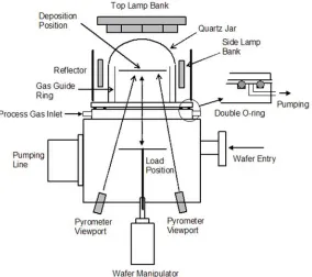
Figure 2-1 A schematic illustration of UHV-RTCVD system used in this work. ... 34
Figure 2-2 The main process chamber (MPC) of the UHV-RTCVD system consists of a quartz
bell jar, a top lamp bank, and a side lamp bank... 35
Figure 2-3 A typical deposition sequence used in Si1-xGex and Si epitaxy. ... 37
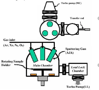
Figure 2-4 Schematic of the UHV RF sputtering system: (a) top view; (b) side view. ... 39
Figure 3-1 XRD spectra of 100nm Si1-xGex film deposited on a crystalline bulk silicon substrate
where x is about 50%. ... 47
Figure 3-2 (a) The C-V characteristic of a MOS capacitor on P-type Si substrate. (b) The
Figure 3-3 High and low-frequency C-V curves show the offset ∆C/Cox due to interface traps. . 53
Figure 3-4 Equivalent circuits for conductance measurements... 55
Figure 3-5 Gp/ω versus ω for a single level, a continuum and experimental data. For all curves:
Dit=1.9×109cm-2eV-1, τit=7×10⁻⁵s ... 57
Figure 3-6 Energy band diagram description of (a) Fowler-Nordheim injection through a
triangular barrier and (b) direct tunneling through a trapezoidal barrier... 60
Figure 3-7 Plot of overall mobility versus effective field limited by various scattering mechanisms.
... 62
Figure 3-8 Schematics of experimental setup to measure (a) gate to channel capacitance for
Split C-V, (b) gate to substrate capacitance, and (c) total gate capacitance; and (d)
gate-to-channel and gate-to-substrate capacitance as a function of gate voltage... 64
Figure 3-9 Schematic of an nMOSFET showing the current components in the Id–Vg
measurement... 67
Figure 3-10 Schematic of (a) the charge pumping measurement configuration; (b) the square
wave pulse used in two level charge pumping... 69
Figure 3-11 Schematic of the waveforms and resulting Icp of (a) the Base Sweep and (b) the
Amplitude Sweep of two level charge pumping measurements... 70
Figure 3-12 Schematic of the waveform used in the three level charge pumping to profile interface
traps with energies between Ec and Ei. ... 72
Figure 4-1 Incubation time plotted as a function of insulator materials... 78
Figure 4-2 XRD scans for the deposited films with same gas flow but different thickness.
Deposition parameters are listed in Table 4-1... 81
Figure 4-3 AFM surface scans of deposited films: (a) epi Si: RMS ~0.17 nm (Z scale 30 nm); (b)
Si1-xGex: RMS ~0.59 nm (Z scale 30 nm); (c) strained Si (9 nm): RMS ~0.75 nm (Z
scale 30 nm); (d) strained Si (15 nm): RMS ~0.60 nm (Z scale 30 nm); (e) strained Si
(20 nm): RMS ~0.62 nm (Z scale 20 nm). ... 85
Figure 4-5 C-V and I-V characteristics of four HfO2 samples whose process conditions are listed
in Table 4-3: (a) C-V data; (b) Jg plotted as a function of voltage across the oxide
(Vox); (c) Jg of SiO2 from reference; (d) deviation of Jg observed from the I-V data of
sample Hf3... 90
Figure 4-6 The XPS spectra of (a) Hf 4f and (b) Si 2p core-levels of two HfO2/Si samples. ... 92
Figure 4-7 The XPS spectra of (a) Hf 4f and (b) Si 2p core-levels of a RTA HfO2/strained Si
sample compared to the HfO2/bulk Si system... 93
Figure 4-8 A TEM image of a strained Si sample with high κ and metal gate electrode stacks. All
layers were labeled in (a) and (b) while details of HfO2 and the interfacial layer were
shown in (c). ... 95
Figure 4-9 A SEM image of selectively deposited SiGe layer confined in the active area,
achieved by S. Chopra working in the same group as the author in NCSU. ... 97
Figure 4-10 Schematic illustration of cross-sections of overlap and non-overlap capacitors... 98
Figure 4-11 Leakage current densities of overlap and non-overlap capacitors with (a) SiO2 and (b)
HfO2 as gate dielectrics. ... 99
Figure 4-12 Raman spectra of strained Si samples with different thicknesses: (a) a typical Raman
spectrum of a strained Si sample; (b) different strain level was achieved by varying
strained Si thickness; (c) Raman peak shifts plotted as a function of strained Si
thickness. ...101
Figure 5-1 C-V curves from MOS capacitors with SiO2 and HfO2 gate dielectrics and TaN gate
electrodes. The measured area is 50µm by 50µm...107
Figure 5-2 (a) Equivalent oxide thickness and (b) leakage current density of SiO2 and HfO2
samples are plotted vs. strained Si thickness. The gate electrodes are TaN. ...108
Figure 5-3 Hysteresis of SiO2 and HfO2 samples are plotted vs. strained Si thickness, with TaN
as the gate electrodes. ...108
Figure 5-4 The density of interface traps (Dit) plotted as a function of (a) the trap energy; (b)
Figure 5-5 Electrical parameters of TaN gate MOS capacitors after RTA plotted vs. strained Si
thickness: (a) leakage current density at 1V beyond VFB; (b) EOT; (c) hysteresis...111
Figure 5-6 Interface trap density (Dit) after RTA is plotted as a function of strained Si thickness.
The gate electrode is TaN. ...112
Figure 5-7 Ge profiles from SIMS show the effect of high temperature process on Ge
out-diffusion. Samples have 20nm strained Si layer. ...114
Figure 5-8 XPS spectrum of Ge 3d core level of a 9nm strained Si/ 3.5nm SiO2 sample with the
oxide removed. ...115
Figure 5-9 The density of interface traps (Dit) plotted as a function of (a) the trap energy; (b) Ge
concentration with varying strained Si thickness. TaN is used as the gate electrode. ..
...116
Figure 5-10 Raman peak shifts plotted vs. strained Si thickness with varying Ge content in the
virtual substrate. ...117
Figure 5-11 SIMS profiles of Si and Ge of two strained Si samples with different Ge content in the
SiGe buffer layer. It can be seen that more Ge out-diffusion into the strained Si
channel would be expected in sample B than in sample A ...118
Figure 5-12 Dit plotted as a function of Raman peak shift with varying Ge content in the SiGe
virtual substrate. Sample A and B refer to the conditions listed in Figure 5-11 ...119
Figure 6-1 Basic electrical characteristics of bulk Si and strained Si (16nm) MOSFETs with
POLY and TaN gate electrodes: (a) C-V curves; (b) drain currents...140
Figure 6-2 Mobilities of polysilicon and TaN metal gates on SiO2 dielectrics extracted by Split
C-V analysis. ...142
Figure 6-3 (a) C-V curves of TaN nMOSFETs on bulk Si or 20nm strained Si with SiO2 or HfO2;
(b) EOT values plotted as a function of strained Si thickness...144
Figure 6-4 Comparison of gate leakage current for strained Si and bulk Si nFETs with SiO2 and
HfO2. ...145
Figure 6-6 Effective mobility of SiO2 nFETs plotted vs. effective field. Three different strained Si thicknesses were employed. Bulk Si nFET was used as a control. ...147
Figure 6-7 Effective mobility of HfO2 nFETs plotted vs. effective field. Three different strained Si
thicknesses were employed. ...148
Figure 6-8 Charge pumping currents plotted vs. base sweep biases for TaN/HfO2 devices on (a)
bulk Si; (b) 9nm strained Si. The measurements were carried out at 100kHz...150
Figure 6-9 Charge pumping currents plotted vs. amplitude sweep biases for TaN/HfO2 devices
on (a) bulk Si; (b) 20nm strained Si. The measurements were carried out at 100kHz. .
...151
Figure 6-10 Dit measured from two level charge pumping at 100kHz for nFETs on SiO2 and HfO2
with different strained Si thickness. ...151
Figure 6-11 Dit extracted from three level charge pumping as a function of (a)bandgap; (b)
strained Si thickness for strained Si MOSFETs with TaN gates on SiO2 and HfO2...
...153
Figure 6-12 Effective electron mobility after Dit corrections for TaN strained Si MOSFETs on SiO2
and HfO2. ...157
Figure 6-13 Effective electron mobility extracted with Dit corrections for nMOSFETs on (a) SiO2
and (b) HfO2...158
Figure 6-14 Peak mobility enhancement factor γ plotted vs. strained Si thickness. ...159
Figure 6-15 Possible sources of scattering in high- κ gate stacks. ...160
Figure 6-16 HfO2 limited mobility component for bulk Si and strained Si devices plotted as a
function of effective field. ...161
Figure 6-17 Peak mobility plotted as a function of temperature for TaN gate MOSFETs on SiO2
and HfO2 dielectrics with bulk Si and/or strained Si channels...162
Figure 6-18 Dit-corrected effective mobility and calculated phonon limited mobility using
Figure 6-19 “Phonon-limited” effective mobility components of n-channel devices plotted as a
function of effective field on bulk Si and strained Si. Theoretical values calculated in
Ref. A and ref. B are also included...165
Figure 6-20 The phonon, surface roughness and interface scattering mobility components of a
strained Si sample simulated by using Hauser’s MOB2D model compared to those of
a bulk Si sample. ...167
Figure 6-21 Modeled peak mobility plotted vs. temperature with different interface scattering
density (I.S.) and surface roughness (S.R.) parameter values extracted from the
List of Tables
Table 1-1 High performance logic technology requirements -- Near Term ... 2
Table 1-2 Potential solutions to improve device performance ... 3
Table 1-3 Effects of stress on the MOSFET performance in different directions for a <110> oriented channel. ... 14
Table 2-1 Typical process conditions for Si and Si1-xGex deposition used in this work... 37
Table 2-2 Metal gate electrode sputtering conditions and rates... 42
Table 2-3 Summary of strained Silicon MOSFET process flow. ... 43
Table 4-1 Summary of XRD extracted Ge concentration in deposited films as a function of film thickness. The deposition temperature was 500°C and the deposition pressure was 700 mTorr maintained by adjusting the throttle valve. ... 81
Table 4-2 Experimental conditions considered in this study to optimize deposition parameters without using the throttle valve... 83
Table 4-3 Process parameters used in HfO2 formation experiments... 87
Table 4-4 Electrical properties extracted from C-V data and leakage current densities before and after RTA of HfO2 samples. ... 88
Table 6-1 Extracted device parameters for SiO2 MOSFETs with polysilicon and TaN gate electrodes. Strained Si (SSi) thickness is the starting thickness before gate oxidation. ...140
Table 6-2 Extracted device parameters of TaN gate MOSFETs on SiO2 and HfO2. ...146
Table 6-3 Constants used to extract average Dit values from two level charge pumping measurement...149
Chapter 1 Introduction
1.1 CMOS Technology Scaling
Integrated circuit (IC) technology has been improving for over 40 years,
following Moore’s Law by consistently scaling the design rules, increasing the chip
and wafer size, and cleverly improving the designs of devices and circuits [1, 2]. For
both memory and logic chips, the speed and density increased exponentially while
the power dissipation and cost per function decreased. For example, the speed of
microprocessors has been doubling approximately every three years, increasing
from 2 MHz for the Intel® 8080 in the mid-1970s to over 1 GHz for the current chips
[3]. Continuous MOSFET scaling resulted in advancing from the ~ 8 µm technology
in 1972 to the current 90 nm technology, which corresponds to a reduction of ~ 0.87
per year [4]. If the scaling continues at this rate, the IC industry will face increasing
difficulties due to the fundamental limits of certain devices and materials.
The Semiconductor Industry Association (SIA) has been publishing roadmaps
since 1992. The most recent 2004 International Technology Roadmap for
Semiconductors (ITRS) predicts the next 14 years [2]. In comparison to the 1999
ITRS [5], one major change is acceleration in the scaling of the physical gate length
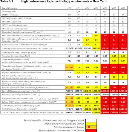
(Lg) driven by the industry’s need to maximize the chip speed [4]. Table 1-1 presents
all the parameters required by High performance logic technology in the next several
Table 1-1 High performance logic technology requirements -- Near Term
For digital circuits, the gate delay is defined as τ =CV /I where C is the gate
capacitance, V is the voltage swing and I is the drive current. While the drive current
is increasing linearly with scaling the transistor off current is increasing exponentially.
Both a large drive current and a small standby power are needed. Device
performance can improve by 1) inducing a larger charge density for a given gate
achieve a shorter channel length; and 4) reducing parasitic capacitances and
parasitic resistances [6]. Table 1-2 summarizes these opportunities/challenges and
corresponding proposed technology options. These options can be classified into
two categories: new materials and new device structures, which are usually related.
Table 1-2 Potential solutions to improve device performance [6].
Source of improvement
Parameters affected Method
Charge
density • S (inverse subthreshold slope)
• Qinv at a fixed Ioff
1. Double-gate FET.
2. Lowered operating temperature.
Carrier
transport •• Mobility (Carrier velocity µeff)
• Ballistic transport
1. Strained silicon.
2. High-mobility and saturation-velocity
materials (e.g., Ge, InGaAs, InP).
3. Reduce mobility degradation factors (e.g., reduced transverse electric field, reduced Coulomb scattering due to dopants, reduced phonon scattering).
4. Shorter channel length.
5. Lowered operating temperature.
Parasitic
resistance • Rext
1. Extended/raised source/drain.
2. Low-barrier Schottky contact.
Parasitic
capacitance •• CCjnGD, CGS, CGB
1. SOI.
2. Double-gate FET.
Ensuring device
scalability to a shorter
channel length
• Generalized scale
length (λ)
• Channel length (Lg)
1. Maintaining good electrostatic control of channel potential (e.g., double-gate FET, ground-plane FET, and ultrathin-body SOI) by controlling the device physical
geometry and providing means to terminate drain electric fields. 2. Sharp doping profiles, halo/pocket
implants.
3. High gate capacitance (thin gate dielectrics, metal gate electrode) to provide strong gate control of channel potential.
As summarized in the table above, strained silicon could be one of the
candidates to enhance the carrier transport. A high dielectric constant (κ) material is
required to achieve low equivalent oxide thickness (EOT). In addition, metal gate
to ensure the device scalability and eliminate problems brought about by polysilicon
gates. All the advantages and current issues of strained silicon, high-κ dielectrics,
and metal gates will be discussed in detail in the following sections.
1.2 Strained Silicon Technology
1.2.1 Why Is Strained Silicon Required for Future CMOS Devices
Alternative channel materials that offer higher carrier mobilities are needed to
improve the carrier transport properties of future MOSFETs. Unfortunately, replacing
Si with a new material does not necessarily provide the performance enhancement
expected from the higher mobility due to other shortcomings or performance
challenges of the new material [7]. This is one of the key reasons behind the recent
excitement over strained Si. Essentially, it is now well established that without
changing the channel material, significant enhancements in device performance are
possible using strained silicon [8-23]. The theory of mobility enhancement in strained
Si is still evolving [10]. The most commonly accepted explanation is that under the
biaxial tensile strain, the six-fold degenerate valleys in Si are split into two groups.
The group with the lower energy is two fold degenerate (labeled as ∆2 in Figure 1-1),
which is the primary contributor to carrier transport at low fields. The in-plane
effective mass of the electrons occupying these bands is approximately equal to the
Si transverse effective mass (mt*=0.19m0). On the other hand, the effective mass
perpendicular to the transport plane is equal to the longitudinal effective mass
(ml*=0.92m0). The schematic representation of the energy ellipses is shown in Figure
1-1[8]. The energy of the conduction-band minima of the four valleys on the in-plane
perpendicular to the plane [24, 25], as shown in Figure 1-2 (a) [26]. The energy
between the two-fold degenerate and the four-fold degenerate valleys, ∆Estrain, is
given by ∆Estrain =0.67xeV , where x is the Ge content of the relaxed Si1-xGex
substrate [9]. It should be noted that even in an unstrained Si MOS inversion layer
there is band splitting between the sub-band energies in the two and the four-fold
valleys due to quantization in the inversion layer. In a strained Si MOS inversion
layer, the band splitting of the conduction band ∆Estrain is superimposed on this
quantization, as schematically shown in Figure 1-2 (b) [26]. The electrons populate
the lower ∆2 valleys with lighter effective mass, which results in the reduction of the
average conductivity effective mass.
Figure 1-1 Schematic representation of the strain induced conduction band splitting in
Figure 1-2 Energy alignment of the Si conduction band with and without the tensile strain
in (a)bulk and (b) inversion layer, respectively.
The other mechanism of mobility enhancement proposed by Takagi et al. [26]
is the suppression of intervalley phonon scattering due to the energy splitting
between the two fold and the four fold valleys. Intervalley phonon scattering is an
inelastic process associated with the absorption or the emission of the relevant
phonons with a large wave vectors. Thus, if the amount of the band splitting between
the two and the four fold valleys becomes larger than the energy of the relevant
phonons, the scattering probability will be significantly reduced. Therefore, better
enhancement of the electron low field mobility will be achieved with higher Ge
content in the relaxed Si1-xGex substrate.
In unstrained material, the valence band maximum is composed of three
bands: the degenerate heavy-hole (HH) and light-hole (LH) bands at k=0, and the
split-off (SO) band which is slightly lower in energy, as shown in Figure 1-3 [12]. The
The hydrostatic stress equally shifts all three valence bands, while the uniaxial
stress lifts the degeneracy between LH and HH bands by lifting the LH band higher
than HH. The SO band is also lowered with respect to the other two bands. This
leads to the population of holes in the energetically favorable LH like band.
Application of stress also changes the shape of the bands as shown in Figure 1-3 (b).
Therefore, due to the band deformation, the in-plane transport mass becomes
smaller and the interband scattering is also suppressed. Thus the hole mobility is
improved.
Figure 1-3 Simplified hole valence band structure for longitudinal in plane direction (a)
unstrained and (b) strained silicon [27].
The main difference between the effects on electron and hole mobilities is
that the mobility of holes can be enhanced only at lower electric fields while the
enhancement can be achieved at higher vertical electric fields for electrons. Fischetti
et al. showed that the loss in hole mobility enhancement at higher fields was due to
reduction in the separation between the light hole and heavy hole bands (∆LH-HH) [28].
Based on the experimental data, it was speculated that this was due to the confining
surface potential operating against the applied biaxial stress and trying to reduce the
silicon devices can improve hole mobility at both low and high electric fields, which
will be presented in section 1.2.3.
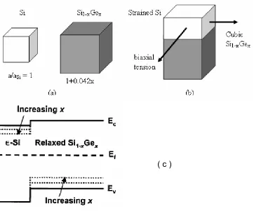
1.2.2 Biaxial Strained Silicon and Device Applications
Strain in Si can be introduced in various ways. The most commonly used
method is to deposit a thin Si epitaxial layer on top of a thick relaxed SiGe buffer
layer [11, 14, 29]. Silicon and germanium, both crystallizing in the diamond lattice,
can form a continuous series of Si1-xGex solid solutions with x ranging from 0 to 1.
The lattice constants are 0.5431 nm for Si and 0.5657 nm for Ge. The lattice
mismatch between Si and Ge, herein referred to as f, is about 4.2 %, which is
sufficiently small. Therefore the deposited first several atomic layers will be strained
to match the substrate and a coherent interface will be formed. The structure stores
a high amount of elastic strain energy because interatomic bond lengths in the
epilayer are stretched or compressed compared to their equilibrium values. At some
epilayer thickness, generally called the critical thickness hc, it becomes energetically
favorable to relieve the elastic strain energy by introducing misfit dislocations and
allowing the epilayer to relax towards its bulk lattice parameter. The critical thickness
has been first calculated by several groups based on different models [30-35]. When
the thickness of Si1-xGex alloy exceeds the critical thickness, the alloy will be called a
“relaxed” Si1-xGex film. The lattice parameter could be calculated according to the
Vegard’s law, assuming the film is fully relaxed:
x a x a
x
aSiGe( )= Si⋅(1− )+ Ge⋅ (1.1)
The primary function of this relaxed SiGe layer is to serve as a “virtual
However it has no impact on the improvement of device performance. The thickness
of strained Si must be relatively thin so that the strain will not be relaxed through
misfit dislocations. Figure 1-4 (c) shows the band offset for a strained-Si film grown
on relaxed (001) SiGe substrate. In this case, a large band offset is obtained in both
the conduction and valence bands relative to the relaxed Si1-xGex layer and is called
a type II band offset [25, 36]. This allows both electron and hole confinements in the
strained Si layer, making it useful for both n- and p-type devices for strained-Si/SiGe
based CMOS technology. The critical thickness of Si layers grown on relaxed
uniform SiGe layers has also been calculated [37].
Figure 1-4 Schematic illustrations of (a) equilibrium lattices and (b) pseudomorphic
strained Si on relaxed SiGe [8] (c) band alignments between strained Si and the relaxed SiGe
virtual substrate[38].
Recent work has provided encouraging experimental data showing the
mobility enhancement with different devices structures, including both n-channel and
p-channel devices. Research on strained Si MOSFETs can be grouped into two
categories: “bulk” strained Si on relaxed SiGe FETs (SS FETs) and strained Si on
relaxed SiGe on insulator FETs (SGOI FETs). Recent work indicates that a
conventional CMOS process flow can be adopted while still achieving the mobility
and current drive enhancement [20]. Fabrication processes such as source/drain
extensions and halos, channel ion implantation, and associated high temperature
activation anneals are shown to have no adverse impact on device characteristics.
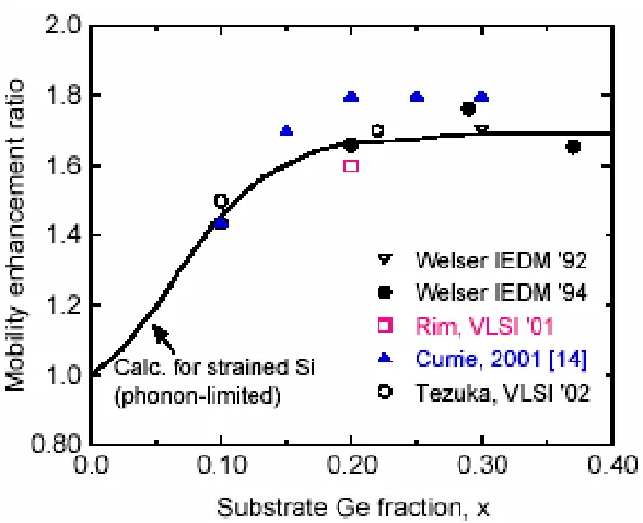
The first strained Si n-MOSFETs were fabricated on relaxed Si0.7Ge0.3
substrates and provided about 70% electron mobility enhancement with a vertical
effective electric field (Eeff) up to 0.6 MV/cm [21]. At a lower VGS, the current drive
enhancement over the unstrained silicon control is as large as 50%, while at VGS =
0.8 V, the current drive of a strained Si device is ~ 35 % higher [6]. Figure 1-5 shows
both the experimental data and the theoretical values of the phonon limited electron
mobility enhancement versus the substrate Ge content [22]. With the Ge content
above 20 %, the mobility enhancement factor, r, saturates near 1.8, in agreement
with calculations of the impact of strain on the mobility. Experiments also indicate
that for electrons, the strain induced mobility enhancement factor is relatively
constant with Eeff. For the same channel length, the current drive enhancements can
be significantly changed due to the variation of doping profiles, strain induced band
Figure 1-5 Measured (symbols) effective mobility enhancement ratios, r, compared to
calculations for the phonon limited MOS mobility (solid line) for strained Si n-MOSFETs [22].
The combination of high mobility strained Si devices with SOI structures will
provide additional advantages such as reduced parasitic capacitances, improved
isolation, and reduced short channel effects. Strained Si-on-insulator (SSOI)
MOSFETs can be fabricated from strained silicon grown on relaxed Si1-xGex
-on-insulator (SGOI) virtual substrates [12, 15-19, 23, 37, 38]. SGOI can be achieved via
several approaches such as “etch-back” and “smart-cut” processes [12, 15-17, 23],
SIMOX technology [14, 18, 37], and Ge condensation techniques [12, 19, 38].
The Si valence banddegeneracy is also split by biaxial tensile strain induced
by growth in relaxed Si1-xGex (~ 40 meV/10 % Ge). Therefore, hole mobility
enhancement can also be obtained with strained Si p-MOSFETs. Generally, larger
strain is required to get valence band splitting, which means higher Ge content is
Figure 1-6 [22] where the hole mobility enhancement is primarily achieved in the low
Eeff range (<1 MV/cm) and the mobility enhancement ratio approaches 1 with the Ge
content below 30 % in the underlying relaxed SiGe substrate. Unlike electron
mobility, hole mobility enhancement is reduced for higher Eeff. To improve the hole
mobility further, the substrate Ge content should be increased. This could be the
solution for the single strained Si channel structures, which is feasible by using
SIMOX and Ge condensation techniques.
Figure 1-6 Comparison of hole mobility enhancement ratios in strained Si p-MOSFETs as
a function of vertical effective field, Eeff. The numbers beside the data are the substrate Ge
percent.
1.2.3 Uniaxial Strained Silicon and Device Applications
There are various methods to induce uniaxial stress, which differ from one
junction structures, and gate electrodes have been reported recently to cause
sufficient local strain, which can alter device characteristics [28, 39-47].
Intel demonstrated strained silicon MOSFETs with uniaxial strain based on
the structure shown in Figure 1-7[39, 40]. Piezoresistance coefficients in silicon were
used to model the behavior of uniaxial stress in MOSFETs. This model is only valid
for small stress values where the mobility enhancement mainly results from the
change in the conductivity effective mass. This is a good assumption since Intel
used low stress levels for its MOSFETs and fewer defects are created requiring less
alteration to the existing technology. Detailed discussions of the effect of mechanical
stress on the mobility can be found in literature [39-41]. A summary of the effects of
various stress components on the channel mobility is listed in Table 1-3. It can be
seen that in order to achieve mobility enhancement for a <110> channel, longitudinal
compressive stress for pMOSFETs and longitudinal tensile and out of plane
compressive stress for nMOSFETs are most effective. Therefore SiGe source/drain
junctions on the PMOS and a tensile capping layer on the NMOS were employed by
Intel to induce strain.
Table 1-3 Effects of stress on the MOSFET performance in different directions for a
<110> oriented channel [39, 41, 42].
Directions NMOS PMOS
Along channel (x) Tension
+ + +
Compression + + + +
Across channel (z) Tension
+ +
Tension + + +
Vertical (y) Compression
+ + + +
Tension +
In addition to achieving a higher hole mobility enhancement at low vertical
electric fields deduced from the piezoresistance coefficients [43], uniaxial strain also
maintains this enhancement at higher electric fields, which has been demonstrated
experimentally. Fischetti et al. has theoretically explained the loss of hole mobility
enhancement at higher fields by using reduced separation between the LH and HH
like bands [28]. However, for uniaxial stress, the confining surface potential does not
reduce the strain induced band separation as it does in the biaxial case. This can be
attributed to the band warping caused by the uniaxial stress to create an
advantageous out of plane effective mass for the top energy band. Therefore, the
hole population in the energetically favorable LH like band would be enhanced and
hence the mobility enhancement at higher fields would be maintained.
For the corresponding NMOS device fabricated by Intel, a nitride capping
layer which created longitudinal tensile and out of plane compressive stress in the
silicon channel was used to obtain the electron mobility enhancement [39]. The
enhancement in performance was shown to be strongly dependent on the thickness
of the capping layer. As shown in Figure 1-8, a capping layer thickness of ~75 nm
Figure 1-8 Electron saturated drive current improvement verses nitride thickness [40].
Texas Instruments (TI) also presented PMOS transistors with a channel
length of 37 nm built on successful integration of a recessed SiGe epitaxial layer at
the drain extension location. Compressive stress induced by the SiGe layer resulted
in 35 % improvement in current drive [44]. Yang et al. reported a high performance
CMOS flow in which nitride contact liners were used as dual stress liners (DSL) to
induce both tensile and compressive stress achieving mobility enhancement for both
electrons and holes. This DSL approach results in 15 % and 32 % effective drive
current enhancement for nFET and pFET, respectively and a saturated drive current
enhancement of 11 % for nFET and 20 % for pFET [45]. Strain Enhancing
Laminated Si3N4 (SELS) was employed by Fujitsu [46] using a new process flow in
which SELS was formed selectively only on the nMOS gate. Multiple layers of Si3N4
currents of 1120µA/µm and 690µA/µm at Vdd=1V/Ioff=100nA/µm were demonstrated
for a 37 nm gate nMOS and a 45 nm gate pMOS, respectively. Uniaxial strain was
also induced by selective epitaxy of silicon carbide (SiC) in the source and drain
(S/D) regions of sub 100nm gate nMOS transistors [47]. The carbon mole fraction
was 1.3 % such that the lattice mismatch between SiC and Si was 0.65%, resulting
in tensile strain along the Si channel and compressive strain normal to the channel.
Both the tensile and compressive stress contributed to substantial electron mobility
enhancement and ~50 % enhancement in drive current was obtained for a gate
length of 50 nm.
1.3 Alternative High Dielectric Constant Gate Insulator Materials
1.3.1 Why Are High κ Dielectrics Required
One of the biggest concerns in modern CMOS technology is the gate
dielectric. Silicon dioxide (SiO2) has been the ideal gate dielectric because of its
amorphous structure, a large band gap of ~ 9 eV, insolubility in water, ability to serve
as a separator between metal conducting layers and silicon substrates, and its
compatibility with Si having low interface state densities [48]. As the gate oxide
begins to scale down to the ultra thin oxide regime, the direct tunneling current
increases [49]. In addition, quantum mechanical effects and the polysilicon depletion
effect can be amplified as the SiO2 thickness is reduced, which results in an
increase in the effective dielectric thickness [50, 51]. Due to these limitations of SiO2,
alternative gate dielectrics with higher dielectric constant are required such that
physically thicker dielectrics can be used to reduce the probability of electrons and
Besides the high permittivity, additional requirements for alternate high-κ
dielectrics include a large band gap for appropriate barrier height, thermodynamic
stability on Si, noncrystalline film morphology, ability to form a high quality interface
with Si (with low fixed charge and low interface charge), and compatibility with gate
electrodes and existing CMOS processing. Current research is focused on
dielectrics with moderate κ since the permittivity must be balanced with the band
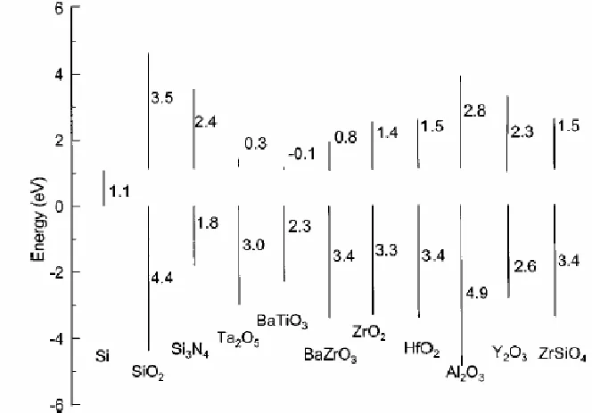
offset, which is the barrier height for tunneling processes. Figure 1-9 shows the key
properties (dielectric constants and band offsets) of potential high-κ dielectric
candidates [52, 53]. Therefore, to achieve low gate leakage, those materials with
band offsets less than 1 eV will not be desirable candidates as gate insulators. Most
of the high-κ metal oxide systems investigated so far have unstable interfaces with
Si. Therefore an interfacial layer is formed which plays a dominant role in the device
electrical properties. It is necessary to study the thermodynamics of these systems
thereby attempting to control the interface between high-κ and Si [54]. Currently,
most of the high-κ materials show Dit of 1011–1012 cm-2-eV-1 and fixed charge
density >1012 cm-2 at the interface, which is higher than the typical midgap interface
density of Si (2 x 1010 cm-2) [55-58]. It is desirable to select a material which remains
amorphous throughout the entire CMOS process since amorphous films exhibit
isotropic electrical properties and will not suffer from grain boundaries. The last
concern is the compatibility, i.e. the deposition process for high-κ dielectrics must be
compatible with conventional CMOS processing based on the consideration of cost
Figure 1-9 Band offset calculations for a number of potential high-κ gate dielectric
materials [52, 53].
1.3.2 Hafnium Based Dielectrics
For the past several years, HfO2 and its silicates have received significant
attention as alternative gate dielectrics due to their thermodynamic stability on Si
and their large barrier heights [56, 59-61]. Lee et al. achieved an ultra thin HfO2 gate
dielectric with 0.9 nm EOT and a Pt gate using an optimized reactive dc magnetron
sputtering process [56]. It is found that the dielectric constant of HfO2 was ~28 and
that the EOT was stable up to 700 ºC. Lee et al. also reported a 1.04 nm EOT HfO2
withpolysilicon gate without any barrier layer [59]. They reported that their HfO2 film
remained high quality after high temperature dopant activation (950 ºC for 30
seconds) and had very low leakage current (0.23 mA/cm2 at Vg = 1 V). Wilk et al.
reported an EOT less than 1.8 nm for a 5 nm Hf6Si29O65 film, which yields a dielectric
best candidate as the gate insulator for 65 nm gate length CMOS. Researchers are
still continuously searching for a material which can fulfill all the gate dielectric
requirements.
1.3.3 Additional Problems with High κ Dielectrics
Challenges arise from the processing and integration of high-κ dielectrics,
especially during those steps preformed at high temperature. The intrinsic limitation
of high-κ dielectrics is that a SiO2 rich interfacial layer will be formed during the
deposition of high-κ on Si, which makes it very difficult to scale the EOT. Recently,
reports of nitrogen based materials and nitrogen annealing have shown the
decrease or elimination of the interfacial layer [62-65]. Thermal stability is another
key requirement for high-κ dielectrics since junction activation is always performed at
a high temperature in conventional CMOS processing. The possible formation of
silicates between the dielectric and Si substrate as well as other probable reactions
between high-κ dielectric with metal gates will inevitably increase the EOT and have
other adverse impacts on the channel. High temperature processes can also change
the film morphology of high-κ dielectrics, resulting in crystalline or polycrystalline
materials and thus increased leakage.
A lot of attention has been placed on the mechanisms of mobility degradation
in high-κ devices. NMOS device mobility degradation is a more significant problem
than that of PMOS degradation. Fischetti et al. reported that the high permittivity of
materials like HfO2 and ZrO2 result in the presence of a large part of soft optical
phonons providing a long-range scattering of electrons in the Si inversion layer [66].
unavoidable scattering mechanism. Remote charge scattering may be another
component limiting the carrier mobility in high-κ devices [67]. An in depth study to
understand these additional scattering mechanisms in high-κ gate stacks is
necessary to minimize the mobility degradation.
1.4 Metal Gate Electrodes
1.4.1 Why Do We Need Metal Gates
There are several limitations of the present polysilicon gate for submicron
CMOS technology [68]. Modern CMOS processing uses n+ polysilicon gates for
NMOS and p+ polysilicon gates for PMOS, which is normally achieved by ion
implantation and subsequent annealing. During the doping process, dopant
penetration into the thin gate dielectric may occur, especially for boron, and can shift
the device threshold voltage. For deep submicron devices, ultra shallow junctions
are required. Therefore, both the implantation energy and the dopant activation
temperature are reduced, resulting in a low active dopant concentration in the
externally doped polysilicon. The doping level of polysilicon can also be reduced due
to dopant segregation during silicidation and dopant evaporation during activation
annealing [69]. A polysilicon depletion layer is formed at the polysilicon/gate oxide
interface and can decrease both the drive current and transconductance of the
transistor [69]. The poly-Si depletion becomes more severe as the effective dielectric
thickness is reduced. Also, the sheet resistance of the polysilicon gate can be high
because of the scaling of polysilicon thickness which then limits the MOSFET circuit
speed. Replacing gate electrodes with metal gates will be able to eliminate these
Furthermore, Hobbs et al. have reported that Fermi level pinning problems
occur when polysilicon gate electrodes are deposited on high-κ dielectrics [70]. For
Hf based dielectrics, the interfacial Si-Hf bonds create dipoles which pin the Fermi
level right below the polysilicon conduction band, hence increasing the threshold
voltage. Therefore, metal gate electrodes are required for alternative gate dielectrics.
1.4.2 Current Candidates: Advantages and Problems
Candidates for new metal electrodes are required to have good thermal and
chemical stability, as well as process compatibility with current CMOS technology
and future high-κ dielectrics. A desirable metal gate should have an appropriate
work function for NMOS or PMOS devices. Therefore, the work function needs to be
within 0.2 eV of the conduction and valence band edges of Si [71]. In addition, a low
diffusivity to oxygen and other dopants of the metal gate is necessary. Dual metal
gates or midgap metal gate electrodes can be used in CMOS processing. There has
been research on fabricating CMOS with a single midgap metal gate to simplify the
process. However, due to the tradeoff of low channel doping requested by low
threshold voltage and control of short channel effects, the mid-gap metal gate is not
suitable for submicron devices [72].
Work functions of different metals have been measured by evaluating the flat
band voltages on SiO2, ZrO2 and ZrSiO4 [71]. It was found that the work functions of
Al, Ta, Mo, Ti, Hf, and Zr were near the conduction band of Si, hence they could be
potential candidates for NMOS. On the other hand, the work functions of Pt, Ru, Rh,
Co, Pb, and RuO2 were near the valance band, so these metals appear to be
as WNx, TiNx, TaNx, TaSixNy, which may be able to act as good metal electrodes.
Elemental metals with lower work functions were found to have problems with
stability due to high free energy of formation [62], while high work function metals
provide better stability, but may have adhesion issues.
1.5 Advanced Gate Stacks on Strained Silicon and Current Challenges
1.5.1 Strained Silicon with Novel Gate Stacks
K. Rim et al. first reported the experimental data on the integration of biaxial
strained Si and high-κ gate dielectrics [20]. The strained Si nMOSFETs with HfO2
exhibited 60 % higher mobility than the unstrained Si device with HfO2 and 30 %
higher mobility than the conventional unstrained Si with SiO2 when compared with
the universal MOSFET mobility model [26]. At a given Eeff, the gate leakage current
of the HfO2/strained Si device is significantly reduced while the mobility is enhanced
compared to the conventional SiO2/unstrained Si device.
Datta et al. demonstrated the integration of strained Si NMOS with HfO2 and
TiN metal gate showing enhanced electron mobility at 1 MV/cm with an ultra-thin
EOT of 1.4 nm without any intentional SiON interfacial buffer layer [73]. Both the
mobility degradation due to additional phonon scattering at the HfO2/Si interface and
the screening of the remote phonon-electron interaction by metal gate electrodes
were investigated experimentally.
Strained Si NMOS devices with a NiSi FUSI gate were presented by Xiang et
al. for the first time [74]. NiSi gate electrode is Ni rich although it is a stoichometric
monosilicide close to the gate dielectric. Strained Si was grown on relaxed SiGe and
enhancement was shown without any degradation in gate oxide integrity. Krivokapic
et al. demonstrated the strained Si devices by using ultra thin fully depleted SOI with
NiSi metal gates and mesa isolation [75]. From the electrical results, it was
concluded that the channel was under uniaxial compressive stress for wider devices
and tensile stress for narrower devices. About 30% performance improvement was
accomplished in a 75 nm device due to the process induced strain.
1.5.2 Current issues: Process and Device Design
Several issues arise during the fabrication of biaxial strained Si devices.
Thermal stability is the fundamental requirement for strained Si devices since only
the preservation of strain can make any performance improvement possible. Ge
diffusion can be enhanced by strain [76]. Boron diffusion is retarded in strained Si
while arsenic diffusion is enhanced significantly [77]. Other issues related with
integration include the potential strain relaxation during sidewall spacer formation
due to the free boundary formed by reactive ion etching (RIE) [78], as well as the
threshold voltage (Vth) adjustment because of the reduction of Vth in strained Si on
SiGe. For uniaxial strained Si devices, the main consideration is the strain variations
resulting from the processing. Stress in the channel can be affected by many factors
such as the height of polysilicon gate, the sidewall width, and the gate length [79]. It
is also found that the mobility enhancement factor of uniaxial strained Si devices is
dependent on the substrate dopant concentration (Nsub): the higher Nsub, the less
mobility enhancement [80].
There are many important issues that need to be understood before the new
include the interfacial layer formation at the strained Si/high-κ dielectric interface and
the effect of metal gate electrodes on the channel strain. Recently reported strained
Si MOSFETs with advanced gate stacks have shown good performance [20, 73, 74].
In addition, these studies have shown that the mobility degradation commonly
observed with high-κ dielectrics can be partially compensated by employing a
strained Si channel. However, there are additional scattering mechanisms limiting
the mobility enhancement in this system including increased phonon scattering
attributed to HfO2 [73]. It has been shown that additional Coulomb scattering due to
high Dit reduces the hole mobility in p-channel MOSFETs and enhanced phonon
scattering can decrease the electron mobility in n-channel MOSFETs, both due to
the presence of Ge atoms in the channel [81]. Therefore, it is necessary to fully
understand the impact of Ge on the properties of MOSFETs with strained Si
channels, when there is a relaxed Si1-xGex layer in close proximity, which is the
focus of this work.
1.6 Outline of the Dissertation
This research focuses on the fabrication and characterization of strained Si
devices with alternative gate stacks. Chapter 2 provides a description of the
experiments used to fabricate the devices investigated in this work. Chapter 3
presents a detailed introduction to materials analysis and electrical characterization
of advanced strained Si. In chapter 4, both material and electrical characteristics of
epitaxial SiGe and strained Si films as well as the high-κ dielectric (HfO2) are
evaluated. Chapter 5 discusses the electrical properties of strained Si MOS
MOSFETs fabricated with SiO2, HfO2 and/or metal gate electrodes, is given in
Chapter 6. Chapter 7 concludes the research and provides directions of future work
1.7 References
[1] G. E. Moore, "Lithography and the future of Moore's law," presented at
Advances in Resist Technology and Processing XII, 1995.
[2] S. I. A. (SIA), "International Roadmap for Semiconductors 2004 Edition,"
International SEMATECH, Austin, TX 2004.
[3] P. K. Vasudev and P. M. Zeitzoff, "Si-ULSI with a scaled-down future," IEEE
Circuits & Devices, vol. 14, pp. 19-29, 1998.
[4] P. M. Zeitzoff and J. E. Chung, "Weighing in on logic scaling trends," IEEE
Circuits & Devices, vol. 18, pp. 18-27, 2002.
[5] S. I. A. (SIA), "International Roadmap for Semiconductors 1999 Edition,"
International SEMATECH, Austin, TX 1999.
[6] H. S. P. Wong, "Beyond the conventional transistor," IBM Journal of
Research and Development, vol. 46, pp. 133-168, 2002.
[7] M. V. Fischetti and S. E. Laux, "Monte-Carlo Simulation of Transport in
Technologically Significant Semiconductors of the Diamond and Zincblende
Structures .2. Submicrometer Mosfets," IEEE Transactions on Electron
Devices, vol. 38, pp. 650-660, 1991.
[8] K. K. Rim, J. L. Hoyt, and J. F. Gibbons, "Fabrication and analysis of deep
submicron strained-Si N-MOSFET's," IEEE Transactions on Electron Devices,
vol. 47, pp. 1406-1415, 2000.
[9] T. Vogelsang and K. R. Hofmann, "Electron-Transport in Strained Si Layers
on Si1-XGex Substrates," Applied Physics Letters, vol. 63, pp. 186-188, 1993.
[10] M. V. Fischetti and S. E. Laux, "Band structure, deformation potentals, and
carrier mobility in strained Si, Ge, and SiGe alloys," Journal of Applied
Physics, vol. 80, pp. 2234-2252, 1996.
[11] K. Rim, J. L. Hoyt, and J. F. Gibbons, "Transconductance enhancement in deep submicron strained Si n-MOSFETs," presented at Electron Devices Meeting, 1998. IEDM '98 Technical Digest., International, 1998.
[12] S. Takagi, N. Sugiyama, T. Mizuno, T. Tezuka, and A. Kurobe, "Device structure and electrical characteristics of strained-Si-on-insulator
(strained-SOI) MOSFETs," Materials Science and Engineering B-Solid State Materials
for Advanced Technology, vol. 89, pp. 426-434, 2002.
[13] S. Tiwari, M. V. Fischetti, P. M. Mooney, and J. J. Welser, "Hole mobility improvement in silicon-on-insulator and bulk silicon transistors using local strain," presented at Electron Devices Meeting, 1997. Technical Digest., International, 1997.
[14] T. Mizuno, N. Sugiyama, H. Satake, and S. Takagi, "Advanced SOI-MOSFETs with strained-Si channel for high speed CMOS-electron/hole mobility enhancement," presented at VLSI Technology, 2000. Digest of Technical Papers. 2000 Symposium on, 2000.
[16] L. J. Huang, J. O. Chu, D. F. Canaperi, C. P. D'Emic, R. M. Anderson, S. J. Koester, and H. S. P. Wong, "SiGe-on-insulator prepared by wafer bonding
and layer transfer for high-performance field-effect transistors," Applied
Physics Letters, vol. 78, pp. 1267-1269, 2001.
[17] L.-J. Huang, J. O. Chu, S. Goma, C. P. D'Emic, S. J. Koester, D. F. Canaperi, P. M. Mooney, S. A. Cordes, J. L. Speidell, R. M. Anderson, and H.-S. P. Wong, "Carrier mobility enhancement in strained Si-on-insulator fabricated by wafer bonding," presented at VLSI Technology, 2001. Digest of Technical Papers. 2001 Symposium on, 2001.
[18] T. Mizuno, N. Sugiyama, A. Kurobe, and S. Takagi, "Advanced SOI p-MOSFETs with strained-Si channel on SiGe-on-insulator substrate fabricated
by SIMOX technology," IEEE Transactions on Electron Devices, vol. 48, pp.
1612-1618, 2001.
[19] T. Tezuka, N. Sugiyama, and S. Takagi, "Fabrication of strained Si on an
ultrathin SiGe-on-insulator virtual substrate with a high-Ge fraction," Applied
Physics Letters, vol. 79, pp. 1798-1800, 2001.
[20] K. Rim, S. Koester, M. Hargrove, J. Chu, P. M. Mooney, J. Ott, T. Kanarsky, P. Ronsheim, M. Ieong, A. Grill, and H.-S. P. Wong, "Strained Si NMOSFETs for high performance CMOS technology," presented at VLSI Technology, 2001. Digest of Technical Papers. 2001 Symposium on, 2001.
[21] J. Welser, J. L. Hoyt, and J. F. Gibbons, "NMOS and PMOS transistors fabricated in strained silicon/relaxed silicon-germanium structures," presented at Electron Devices Meeting, 1992. Technical Digest., International, 1992. [22] J. L. Hoyt, H. M. Nayfeh, S. Eguchi, I. Aberg, G. Xia, T. Drake, E. A.
Fitzgerald, and D. A. Antoniadis, "Strained silicon MOSFET technology," presented at Electron Devices Meeting, 2002. IEDM '02. Digest. International, 2002.
[23] Z. Y. Cheng, M. T. Currie, C. W. Leitz, G. Taraschi, E. A. Fitzgerald, J. L. Hoyt, and D. A. Antoniadas, "Electron mobility enhancement in strained-Si
n-MOSFETs fabricated on SiGe-on-insulator (SGOI) substrates," IEEE Electron
Device Letters, vol. 22, pp. 321-323, 2001.
[24] R. People, "Physics and Applications of GexSi1-X/Si Strained-Layer
Heterostructures," IEEE Journal of Quantum Electronics, vol. 22, pp.
1696-1710, 1986.
[25] G. Abstreiter, H. Brugger, T. Wolf, H. Jorke, and H. J. Herzog, "Strain-Induced
Two-Dimensional Electron-Gas in Selectively Doped Si/SixGe1-X
Superlattices," Physical Review Letters, vol. 54, pp. 2441-2444, 1985.
[26] S. I. Takagi, J. L. Hoyt, J. J. Welser, and J. F. Gibbons, "Comparative study of phonon-limited mobility of two-dimensional electrons in strained and
unstrained Si metal-oxide-semiconductor field-effect transistors," Journal of
Applied Physics, vol. 80, pp. 1567-1577, 1996.
[27] M. L. Lee and E. A. Fitzgerald, "Hole mobility enhancements in
nanometer-scale strained-silicon heterostructures grown on Ge-rich relaxed Si1-xGex,"
Journal of Applied Physics, vol. 94, pp. 2590-2596, 2003.
Dependence on surface orientation, strain, and silicon thickness," Journal of
Applied Physics, vol. 94, pp. 1079-1095, 2003.
[29] J. Welser, J. L. Hoyt, S. Takagi, and J. F. Gibbons, "Strain dependence of the performance enhancement in strained-Si n-MOSFETs," presented at Electron Devices Meeting, 1994. Technical Digest., International, 1994.
[30] J. H. Vandermerwe, "Crystal Interfaces .2. Finite Overgrowths," Journal of
Applied Physics, vol. 34, pp. 123-&, 1963.
[31] J. W. Matthews and A. E. Blakeslee, "Defects in Epitaxial Multilayers .1. Misfit
Dislocations," Journal of Crystal Growth, vol. 27, pp. 118-125, 1974.
[32] J. W. Matthews, "Defects Associated with Accommodation of Misfit between
Crystals," Journal of Vacuum Science & Technology, vol. 12, pp. 126-133,
1975.
[33] D. J. Eaglesham, E. P. Kvam, D. M. Maher, C. J. Humphreys, G. S. Green, B. K. Tanner, and J. C. Bean, "X-Ray Topography of the Coherency Breakdown in GexSi1-X/Si(100)," Applied Physics Letters, vol. 53, pp. 2083-2085, 1988.
[34] R. People and J. C. Bean, "Calculation of Critical Layer Thickness Versus
Lattice Mismatch for GexSi1-X/Si Strained-Layer Heterostructures," Applied
Physics Letters, vol. 47, pp. 322-324, 1985.
[35] J. C. Bean, L. C. Feldman, A. T. Fiory, S. Nakahara, and I. K. Robinson,
"GexSi1-X/Si Strained-Layer Superlattice Grown by Molecular-Beam Epitaxy,"
Journal of Vacuum Science & Technology A-Vacuum Surfaces and Films, vol.
2, pp. 436-440, 1984.
[36] C. G. Van de Walle and R. M. Martin, "Theoretical calculations of
heterojunction discontinuities in the Si/Ge system," Physical Review B, vol. 34,
pp. 5621 - 5634, 1986.
[37] S. B. Samavedam, W. J. Taylor, J. M. Grant, J. A. Smith, P. J. Tobin, A. Dip, A. M. Phillips, and R. Liu, "Relaxation of strained Si layers grown on SiGe
buffers," Journal of Vacuum Science & Technology B, vol. 17, pp. 1424-1429,
1999.
[38] M. L. Lee, E. A. Fitzgerald, M. T. Bulsara, M. T. Currie, and A. Lochtefeld, "Strained Si, SiGe, and Ge channels for high-mobility
metal-oxide-semiconductor field-effect transistors," Journal of Applied Physics, vol. 97, pp.
-, 2005.
[39] N. Sugiyama, T. Mizuno, S. Takagi, M. Koike, and A. Kurobe, "Formation of
strained-silicon layer on thin relaxed-SiGe/SiO2/Si structure using SIMOX
technology," Thin Solid Films, vol. 369, pp. 199-202, 2000.
[40] T. Tezuka, N. Sugiyama, and S. Takagi, "Fabrication of a strained is on
sub-10-nm-thick SiGe-on-insulator virtual substrate," Materials Science and
Engineering B-Solid State Materials for Advanced Technology, vol. 89, pp.
360-363, 2002.
Wang, C. Weber, and M. Bohr, "A 90 nm logic technology featuring 50 nm strained silicon channel transistors, 7 layers of Cu interconnects, low k ILD,
and 1 µm2 SRAM cell," presented at Electron Devices Meeting, 2002. IEDM
'02. Digest. International, 2002.
[42] T. Ghani, M. Armstrong, C. Auth, M. Bost, P. Charvat, G. Glass, T. Hoffmann, K. Johnson, C. Kenyon, J. Klaus, B. McIntyre, K. Mistry, A. Murthy, J. Sandford, M. Silberstein, S. Sivakumar, P. Smith, K. Zawadzki, S. Thompson, and M. Bohr, "A 90nm high volume manufacturing logic technology featuring novel 45nm gate length strained silicon CMOS transistors," presented at Electron Devices Meeting, 2003. IEDM '03 Technical Digest. IEEE International, 2003.
[43] V. Moroz, X. P. Xu, D. Pramanik, F. Nouri, and Z. Krivokapic, "Analyzing
strained-silicon options for stress-engineering transistors," Solid State
Technology, vol. 47, pp. 49-+, 2004.
[44] M. Ieong, B. Doris, J. Kedzierski, Z. Ren, K. Rim, M. Yang, H. Shang, and L.
Chang, "Device and Substrate Design for Sub-10nm Mosfets," Proc. of
Electrochem. Soc., 2004.
[45] S. E. Thompson, M. Armstrong, C. Auth, M. Alavi, M. Buehler, R. Chau, S. Cea, T. Ghani, G. Glass, T. Hoffman, C. H. Jan, C. Kenyon, J. Klaus, K. Kuhn, Z. Y. Ma, B. Mcintyre, K. Mistry, A. Murthy, B. Obradovic, R. Nagisetty, P. Nguyen, S. Sivakumar, R. Shaheed, L. Shiften, B. Tufts, S. Tyagi, M. Bohr,
and Y. El-Mansy, "A 90-nm logic technology featuring strained-silicon," IEEE
Transactions on Electron Devices, vol. 51, pp. 1790-1797, 2004.
[46] P. R. Chidambaram, B. A. Smith, L. H. Hall, H. Bu, S. Chakravarthi, Y. Kim, A. V. Samoilov, A. T. Kim, P. J. Jones, R. B. Irwin, M. J. Kim, A. L. P. Rotondaro, C. F. Machala, and D. T. Grider, "35% drive current improvement from recessed-SiGe drain extensions on 37 nm gate length PMOS," presented at VLSI Technology, 2004. Digest of Technical Papers. 2004 Symposium on, 2004.
[47] H. S. Yang, R. Malik, S. Narasimha, Y. Li, R. Divakaruni, P. Agnello, S. Allen, A. Antreasyan, J. C. Arnold, K. Bandy, M. Belyansky, A. Bonnoit, G. Bronner, V. Chan, X. Chen, Z. Chen, D. Chidambarrao, A. Chou, W. Clark, S. W. Crowder, B. Engel, H. Harifuchi, S. F. Huang, R. Jagannathan, F. F. Jannin, Y. Kohyama, H. Kuroda, C. W. Lai, H. K. Lee, W.-H. Lee, E. H. Lim, W. Lai, A. Mallikarjunan, K. Matsumoto, A. McKnight, J. Nayak, H. Y. Ng, S. Panda, R. Rengarajart, M. Steigerwalt, S. Subbanna, K. Subranumian, J. Sudijono, G. Sudo, S.-P. Sun, B. Tessier, Y. Tayoshima, P. Tran, R. Wise, R. Wong, I. Y. Yang, C. H. Wann, and L. T. Su, "Dual stress liner for high performance sub-45nm gate length SOI CMOS manufacturing," presented at Electron Devices Meeting, 2004. IEDM Technical Digest. IEEE International, 2004.
at Electron Devices Meeting, 2004. IEDM Technical Digest. IEEE International, 2004.
[49] K. W. Ang, K. J. Chui, V. Bliznetsov, A. Du, N. Balasubramanian, M. F. Li, G. Samudra, and Y.-C. Yee, "Enhanced performance in 50 nm N-MOSFETs with silicon-carbon source/drain regions," presented at Electron Devices Meeting, 2004. IEDM Technical Digest. IEEE International, 2004.
[50] H. R. Huff, A. Hou, C. Lim, Y. Kim, J. Barnett, G. Bersuker, G. A. Brown, C. D. Young, P. M. Zeitzoff, J. Gutt, P. Lysaght, M. I. Gardner, and R. W. Murto,
"High-κ gate stacks for planar, scaled CMOS integrated circuits,"
Microelectronic Engineering, vol. 69, pp. 152-167, 2003.
[51] S. H. Lo, D. A. Buchanan, Y. Taur, and W. Wang, "Quantum-mechanical modeling of electron tunneling current from the inversion layer of
ultra-thin-oxide nMOSFET's," IEEE Electron Device Letters, vol. 18, pp. 209-211, 1997.
[52] W. K. Henson, K. Z. Ahmed, E. M. Vogel, J. R. Hauser, J. J. Wortman, R. D. Venables, M. Xu, and D. Venables, "Estimating oxide thickness of tunnel oxides down to 1.4 nm using conventional capacitance-voltage
measurements on MOS capacitors," IEEE Electron Device Letters, vol. 20, pp.
179-181, 1999.
[53] C. A. Richter, A. R. Hefner, and E. M. Vogel, "A comparison of
quantum-mechanical capacitance-voltage simulators," IEEE Electron Device Letters,
vol. 22, pp. 35-37, 2001.
[54] J. Robertson and C. W. Chen, "Schottky barrier heights of tantalum oxide, barium strontium titanate, lead titanate, and strontium bismuth tantalate,"
Applied Physics Letters, vol. 74, pp. 1168-1170, 1999.
[55] J. Robertson,
![Table 1-2 Potential solutions to improve device performance [6].](https://thumb-us.123doks.com/thumbv2/123dok_us/1204930.1151292/20.595.88.527.245.611/table-potential-solutions-improve-device-performance.webp)

![Figure 1-8 Electron saturated drive current improvement verses nitride thickness [40]](https://thumb-us.123doks.com/thumbv2/123dok_us/1204930.1151292/32.595.156.444.112.325/figure-electron-saturated-current-improvement-verses-nitride-thickness.webp)