A Theoretical Study of the Atomic and Electronic
Structures of Three Prospective Atomic Scale Wire
Systems
Stephen Andrew Shevlin
University College London
PhD Thesis
ProQuest Number: U643743
All rights reserved
INFORMATION TO ALL USERS
The quality of this reproduction is dependent upon the quality of the copy submitted. In the unlikely event that the author did not send a complete manuscript and there are missing pages, these will be noted. Also, if material had to be removed,
a note will indicate the deletion.
uest.
ProQuest U643743
Published by ProQuest LLC(2016). Copyright of the Dissertation is held by the Author. All rights reserved.
This work is protected against unauthorized copying under Title 17, United States Code. Microform Edition © ProQuest LLC.
ProQuest LLC
789 East Eisenhower Parkway P.O. Box 1346
A b stra c t
The structural and electronic properties of several candidate atomic scale wires are anal
ysed. Three candidates are studied; the trans-polyacetylene molecule, the silicon line
on the (001) face of cubic silicon carbide (the ( n x2) series of reconstructions) and the
indium chain on the (111) face of silicon carbide (the (4x1) reconstruction). We use the
polyacetylene molecule as a test-bed for the techniques th at we use to calculate transport
properties in an empirically based tight-binding Hamiltonian (the SSH Hamiltonian). We
calculate the transport properties of wires th at show evidence of a strong coupling of the
electronic degrees of freedom to the phonon degrees of freedom (Peierls distorted wires).
The structure of the (nx2) series of silicon lines (composed of the (3x2) reconstruction
which forms the line and the c(4x2) reconstruction which forms the surface the line
resides on) are modelled in a supercell geometry using ab initio plane-wave calculations
in the Local-Density-Approximation and an ab initio Density Functional Theory based
tight-binding technique. We found th at the thermodynamically favoured model for the
(3x2) reconstruction was the Two-Adlayer-Asymmetric-Dimer Model (with IML of Si
adatoms) and the favoured model for the c(4x2) reconstruction is the Additional-Dimer-
Row-Model (with 0.5ML of Si adatoms). In the tight-binding approximation the line was
found to undergo a Peierls-like transition and holes are observed to form polaron-like
defects. The transport properties of the line are also calculated.
Finally we find which of the two models of the S i(lll)-(4 x 1)-In reconstruction is ther
modynamically favoured in a supercell geometry. We use ab initio plane wave techniques
in the Local-Density-Approximation, and calculate and compare the electronic structure
of the two models with respect to the characteristic energies for electron dispersion along
and across the chain structures. We also consider the effects of electronic structure on
Preface
This thesis is an account of the work th at waa performed by the author from the period
October 1997 to February 2001 under the supervision of Dr. A. J. Fisher and Dr. A. H.
Harker. It has not been previously submitted to this or any other university. P arts of
this thesis have been published or are in press, these papers are listed below.
1. Modelling of the pSiC (O O l) (3x2) surface reconstruction, S. A. Shevlin and A. J. Fisher, App. Surf. Sci. 162-163, 94 (2000)
2. Modelling the c(4 x 2) reconstruction of ^ - S iC (001), S. A. Shevlin and A. J. Fisher, Phys. Rev. B 62, 6904 (2000)
3. The series of (n x 2 ) Si-rich reconstructions of fi-SiC(OOl): a prospective atomic wire?, S. A. Shevlin, A. J. Fisher and E. Hernândez, Phys. Rev. B. 63, 195306, (2001)
4. Coherent electron-phonon coupling and polaron-like transport in molecular wires,
C on ten ts
1 In tro d u ctio n : T h e n a n o sca le: B a s ic p h y sics a n d d e v ic e s 11
1.1 An Introduction to the nanoworld ... 11
1.1.1 Motivation: Why are people interested in t h i s ? ... 11
1.1.2 Im portant length s c a l e s ... 13
1.2 Devices th a t can be manufactured at the nan o scale... 17
1.3 Candidate atomic scale w i r e s ... 24
1.4 Theoretical c o n c e p ts ... 28
1.5 Concluding r e m a r k s ... 34
2 T h e o r y 35 2.1 Modelling systems: Density Functional T h e o r y ... 35
2.1.1 Introduction ... 35
2.1.2 The validity of the L D A ... 38
2.1.3 Varieties of DPT m e t h o d ... 39
2.1.4 The PAW method: W av efu n ctio n s... 43
2.1.5 The PAW method: Operators and e n e r g i e s ... 45
2.2 Modelling systems: Tight-Binding ... 48
2.3 Transport in atomic scale wires: An o v e rv ie w ... 53
2.3.1 Introduction ... 53
2.3.2 Where does resistance come f r o m ? ... 56
2.3.3 Measurement issues ... 59
2.3.4 Calculating the transmission p ro b ab ility ... 61
2.3.5 Size e f f e c t s ... 64
3 T h e P o ly a c e ty le n e m o lec u le : A n id e a l t e s t b e d for s tu d ie s o f a to m ic
sc a le w ire s 73
3.1 Background In fo rm a tio n ... 74
3.2 The Su-Schrieffer-Heeger (SSH) Hamiltonian ... 76
3.3 Calculating phonon modes, which ones are im p o r ta n t? ... 81
3.4 Calculation of electron-phonon c o u p lin g ... 87
3.5 Transport properties: A brief d isc u s s io n ... 89
3.6 Conclusion ... 91
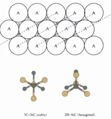
4 S ilico n carbid e: A b in itio s tu d ie s o f th e ( 3 x 2 ) a n d c ( 4 x 2 ) su rfa ces 9 2 4.1 Review of silicon c a rb id e ... 93
4.1.1 Background information on silicon c a rb id e ... 93
4.1.2 The (nx2) series of reconstructions (silicon atomic lines): Physical characteristics and method of f o rm a tio n ... 96
4.1.3 Models of the (3x2) reconstruction and relevant experimental evi dence ... 99
4.1.4 Models of the c(4x2) reconstruction and relevant experimental ev idence ... 105
4.2 Ab initio simulations of the (3x2) rec o n stru c tio n ... 108
4.2.1 General p o i n t s ...108
4.2.2 Simulations of the ADRM model: Physical p r o p e r t ie s ...112
4.2.3 Simulations of the DDRM model: Physical p r o p e r t ie s ...113
4.2.4 Simulations of the TAADM model: Physical properties ...114
4.2.5 Simulations of the ADRM model: Electronic p r o p e r t ie s ... 115
4.2.6 Simulations of the DDRM model: Electronic p r o p e r t ie s ... 117
4.2.7 Simulations of the TAADM model: Electronic properties ...120
4.2.8 Thermodynamic results: Which (3x2) model is fa v o u re d ? 122 4.3 Ab initio simulations of the c(4x2) reconstruction ... 125
4.3.1 Simulations of the AUDD model: Physical properties... 125
4.3.2 Simulations of the MRAD model: Physical p r o p e r t ie s ... 125
4.3.3 Simulations of the AUDD model: Electronic properties...125
4.3.4 Simulations of the MRAD model: Electronic p r o p e r t ie s ...127
4.4 C o n clusions...129
5 S ilico n carb id e: T ig h t-b in d in g a n a ly s is o f t h e str u c tu r e o f th e (n x 2 ) s e r ie s o f r e c o n s tr u c tio n s 133 5.1 Tight-binding: F o rm a lis m ...134
5.1.1 Tight-binding: P a ra m e te ris a tio n ... 134
5.1.2 Tight-binding: T e s t s ... 135
5.1.3 Tight-binding: Correspondence with D PT r e s u lts ... 136
5.2 Structural properties of the (nx2) s e r i e s ... 138
5.2.1 Variation of line structure with n ... 139
5.2.2 Thermodynamic r e s u l t s ...141
5.3 Electronic properties of the ( n x2) s e r i e s ... 141
5.3.1 Variation of bandgap and HOMO state with n ... 141
5.3.2 Density m atrix a n a ly s i s ...144
5.3.3 Proposed mechanism of structural transition for the metastable reconstruction ... 148
5.4 Discussion on the ground-state and m etastable s tr u c t u r e s ... 149
5.5 Larger unit cells: (7x4) unit c e l l ... 150
5.5.1 Structural properties of the (7x4) unit c e l l ... 150
5.5.2 Electronic properties of the (7x4) unit cell ... 152
5.5.3 Density m atrix a n a ly s i s ...153
5.6 C onclu sio n s...155
6 T ra n sp o r t p r o p e r tie s o f th e silic o n lin e s 158 6.1 Effects of charge injection into s y s t e m ... 159
6.1.1 Structural effects of charge injection: Polaron fo rm a tio n ... 159
6.1.2 Effect of polaron formation on electronic s t r u c t u r e ...162
6.2 Which phonon modes couple strongly to the p o l a r o n ? ... 165
6.2.1 Calculation of phonon modes: Formalism and t e s t s ... 165
6.2.2 Huang-Rhys factor a n a ly s is ... 167
6.3 Electron-phonon c o u p lin g ... 171
6.4 Transport p r o p e r tie s ...173
7 A b in itio s tu d y o f th e In a to m ic ch a in o n th e (1 1 1 ) face o f s ilic o n 178
7.1 Background in fo rm a tio n ... 179
7.1.1 The S i(4xl)-In reconstruction ... 179
7.1.2 Models ...182
7.2 PAW simulations: T e s t s ... 186
7.2.1 Projector test: Lattice parameters of Si and I n A s ... 186
7.2.2 Simulation of the (\/3 x \/3 )S i(lll)-In r e c o n s tru c tio n ... 188
7.3 Ab initio simulations of the (4x1) unit cell: General p o i n t s ...190
7.4 Simulation of the Bunk m o d e l... 191
7.4.1 Physical s t r u c t u r e ... 191
7.4.2 Electronic s t r u c t u r e ... 192
7.5 Simulation of the Saranin model ...195
7.5.1 Physical s t r u c t u r e ... 195
7.5.2 Electronic s t r u c t u r e ... 196
7.6 Thermodynamic results: Which model is favoured?...198
7.7 C on clu sio n s...201
8 C o n c lu sio n s an d s u g g e stio n s for fu rth e r w ork 203 8.1 The polyacetylene m o le c u le ...203
8.1.1 C onclusions... 203
8.1.2 Suggestions for further w ork...204
8.2 The silicon lines on silicon c a r b i d e ...206
8.2.1 C onclusions... 206
8.2.2 Suggestions for further w ork...208
8.3 Indium atomic chains on silico n ...211
8.3.1 C onclusions... 211
8.3.2 Suggestions for further w ork... 212
8.4 Final re m a rk s ... 214
A B in d in g e n e r g y in th e tig h t-b in d in g b o n d form 216
B V a lid ity o f a p p r o x im a tio n s u sed in c a lc u la tio n o f tr a n sp o rt? 218
List o f Tables
4.1 Summary of the ability of different models to match experiments. + in
dicates agreement with the experiment, - indicates disagreement with ex
periment and o indicates ambivalent agreement with experiment.
104
4.2 Summary of the ability of different models to match experiments and the
ory considerations. + indicates agreement with the experiment, - indicates
disagreement with experiment and o indicates ambivalent agreement with
experiment.
107
4.3 Equilibrium bond lengths for the addimers and buckling of addimers (mag
nitude) in our total energy calculations and length of dimers in the ter
minating or surface layer. All distances are in Â. See Figures 4.6-4.0 for
information on the nomenclature.
113
4.4 ‘Dispersion’ of HOMO state along [110] (F — J ') and [110] (F — J) direc
tions, for various models. Also shown are values found in the literature.
All values are in eV.
115
4.5 Equilibrium bond lengths for the addimers and dimers in the terminating
or surface layer and amount of buckling (magnitude) found in our total
energy calculations. All distances are in Â. See Figures 4.10 and 4.11 for
more.
5.1 Structure of the various (3 x 2) models as found in our tight-binding scheme
and how they compare to DFT simulations. See Figures 4.6-4.9 for the
meaning of labels. Az refers to the buckle of an addimer. All distances
are in Â.
137
5.2 The addimer structure of our two structures of the (7x2) unit cell; the
ground-state (GS) and metastable state (MS). We also show the buckling
of the addimers. See Figure 5.3 for the definition of oi — 05.
141
5.3 The variation of electronic structure with n for the ground-state system.
We show the dispersion of the HOMO state along the x n and x2 direc
tions and the range of band gap. All units are in eV.
142
5.4 The variation of electronic structure with n for the metastable state sys
tem. We show the dispersion of the HOMO state along the x n and x2
directions and the range of band gap. All units are in eV.
143
5.5 Dispersion of the LUMO state for the metastable structure in eV.
143
5.6 Dispersion of the LUMO state for the ground-state structure in eV.
144
5.7 Dispersion for the HOMO (and LUMO in brackets) states for the “metastable”
structures before and after dimérisation along the x7 and x4 directions
and the range of the HOMO-LUMO gap in eV. We present results for the
flat addimer (top pair) and buckled addimer structures (bottom pair).
153
6.1 Significant Huang-Rhys factors for hole polaron system. Phonon modes
are arranged in increasing frequency (there are 144 phonon modes in total). 168
6.2 Significant Huang-Rhys factors for electron polaron system. Phonon modes
7.1 Summary of the ability of different models to match experiments. + indi
cate agreement with the experiment, - indicates disagreement with exper
iment and o indicates ambivalent agreement with experiment...186
7.2 Ekjuilibrium bond lengths for the indium and silicon addimers. All dis
A cknow ledgem ents
This thesis is the distillation of over three years of work as a PhD student at the Con densed M atter and Materials Physics group in the Department of Physics at University College London. Quite obviously, for these three years I was not a solitary figure who concentrated on his work to the exclusion of everything else (disregarding appearances to the contrary). Therefore it is my great pleasure to acknowledge everyone who has contributed something to the gestation of this thesis, either providing scientific help or personal help (also known as “buying me a pint”).
Firstly I should like to thank my doctoral supervisors, A n d re w F is h e r and T ony H a rk e r. Both of them have performed above and beyond the call of duty, always willing and able to discuss work when they could, providing able advice and encouragement when I needed it, supporting the route I have taken to write this thesis and always making me understand the physics of what I am doing. Secondly I should like to thank H e rv é N ess for his willingness to answer my questions on the physics of transport at the atomic scale and for the interesting and fruitful discussions we have had. Thirdly I should like to thank E d d ie H e rn a n d e z for letting me play with his TROCADERO code and then letting me (for want of a better word) butcher it to obtain some of my results. The Engineering and Physical Sciences Research Council is also thanked for providing me with the funds to pursue my PhD.
Other people have contributed to the scientific work presented in this thesis, in par ticular I would like to thank G e ra ld D u ja rd in and coworkers for the discussions on the (3x2) surface of silicon carbide and the use of STM images presented in this thesis. Prom the CMMP group I would like to thank D a v id B o w ler for advice on the simulation on various aspects of the silicon lines, M a rs h a ll S to n e h a m for advice and discussions on various aspects of solid state physics. L ev K a n to ro v ic h for always been willing and able to answer my questions on any aspect of physics I was interested in, A lex S h lu g e r for always forcing me to consider the full implications of what I am doing, J o h n H a rd in g for advice on the thermodynamical calculations th at have been performed and W e rn e r H o fer for running several tests th at I have asked him to do.
My housemates over the past few years have contributed significantly towards making this thesis the document it is by making the person who wrote the thing the person he is. A d a m F o s te r shall always be remembered for his interesting tea combinations and his gentle wit regarding my grooming (*I* do not have to suffer the wrath of Finnish barbers), J o n a th a n W asse has always amused me with his skillful food preparations and his support for his football team (you can always defect to the *real* Blues, Birmingham City). H a n n a V eh k am ak i for always amusing me with your observations of UCL and the UK (a CD of my music shall be on the way soon, alternatively you can provide the sound effects yourself), K la a s S te p h a n for always been an agreeable chap and R o sa S ch w an d t for been another person who is trying to finish a thesis off and look for a job at the same time.
is one of the original “Gang of Seven” and has always been up for a laugh, a wander and a drink. L ouise D a s h is another one who was often up for a drink, or an amusing comment (pity about the taste in music though... ). F ran cisco L opez has always been available for a quick chat and has often given useful advice (and nice wine and a few good CD’s). A n d re w S te e r has always been up for letting me misuse his computer for non-academic work (and for always making the coffee). P e t e r Sushko (and Shu H a y a m a and A n d y K e rrid g e and D a n ie l Ucko) are thanked for putting up with various meaningless comments th at I have uttered from time to time in order to get away from the grind of work. A n d re a s M a rk m a n n is thanked for letting me borrow various CD’s of his from time to time. And the group secretary D e n ise O ttle y is thanked for providing sterling support over the last three years.
I have lived a life outside UCL as well, and my life has been impacted by the many people who have (in one sense or another) kept me on the path. R ick has always kept me amused and entertained (did you actually read th at paper?). I a n for coming down to London as well as preparing some very nice meals (let’s not buy quite as much food and wine, eh?). M a tth e w and M a rg a r e t for keeping in touch and offering me lifts (when will the stag night and reception take place?). S u z a n n e and Lee for the good laughs, and J im for the sage advice (and how is Oz?). R ich y and Liz and P a u l for the films in London, the drinks and the deathmatch games. The crews of u m stb 5 and the W E F for the distractions. The A m b lesid e lot for the task of legend. R o b , G rae, R ow ls, J a m , G eorge, E la in e and K e v for the nights out in sunny exotic Tamworth (oh, and Torquay). And the mighty B irm in g h a m C ity for being a constant throughout the three years (constantly in the First Division th at is).
Chapter 1
Introduction: T h e nanoscale:
B asic ph ysics and d evices
1.1
A n In trod u ction to th e nanoworld
1.1.1
M otivation : W h y are p eo p le in ter ested in this?
On writing a diary:
“I do not intend to publish it; I am merely going to record the facts for the
information of God” .
“Don’t you think God knows the facts?”
“Yes, He knows the facts, but he does not know this version of the fa c ts” Leo Szilard in conversation with Hans Bethe.
In the world of the late nineties/early noughts, it is becoming increasingly obvious
to the layman th a t electronic devices are becoming smaller and smaller. The logical
endpoint of this trend of miniaturisation is the development, fabrication, and use of
electronic devices th at function on the atomic scale, th a t is at a length scale of the order
of or less than a nanometre (10~® of a metre).
Current manufacturing and fabrication processes (at an industrial scale) have still not
reached this length scale. But, we can estimate when these processes will reach this level,
atomic scale. In 1965 Gordon Moore of Intel made an analysis of the variation of device
size with time, and found th at there was an exponential decrease in device size (or re
spectively an exponential increase in device performance for a fixed size) with a doubling
time of two years (this has since changed to a doubling time of eighteen months). This
means that we can predict th at by, approximately, the year 2017 electronic devices will
be fabricated at the atomic scale [1]. It is thus extremely important from a technological
viewpoint to understand how electronic devices will perform at the atomic scale. It is
also important to devise new types of devices th at can function at an economical price at
this length scale. The current CMOS technologies cannot be scaled all the way down to
the atomic scale for two reasons: firstly that at a critical thickness of semiconductor film
electrons can tunnel through the film thus destroying device functionality, and secondly
even if it were possible to work around this limitation the cost of constructing a fabri
cation plant to manufacture these devices with the desired purity from defects would be
prohibitively expensive, on the order of the Gross Domestic Product of a large country
(see the SIA roadmap for more information [1]).
The behaviour of devices which can function at the atomic scale was first discussed
about forty years ago, by the physicist Richard Feynman, in his seminal lecture “There’s
Plenty of Room at the Bottom” [2]. In this seminar he mentions the capability of electron
beam lithography to etch material at the atomic scale [3], the possibilities of writing and
manipulating information at the molecular level (we ourselves are living proof that this
is possible, as DNA and mRNA molecules store and manipulate information respectively
[4]), the possibility of creating atomic scale computers [5] and the possibility that we
can engineer the properties of materials by altering their structure at the atomic scale
[6, 7, 8],
One other possibility th at Feynman mentioned was th at at this length scale, the
properties of devices can be radically different from devices at larger length scales. There
can be several reasons for this. Firstly, th at at the atomic length scale, the atomic
structure of the device is of critical importance. Defects in the device can dominate
device performance, which means that the manufacture of these atomic scale devices
must be to a very high tolerance (of course, devices could be designed th at use these
defects to their advantage, but one would still have to make certain th at one had the
physical phenomena, for instance to a magnetic field (the Aharonov-Bohm effect) [9],
or to phonons (lattice vibrations) [10, 11, 12, 13, 14, 15, 16, 17, 18, 19, 20, 21, 22] or
electron-electron interactions may be important [23].
Finally, if one were performing logic operations, in theory it is possible to utilize
entanglement at this length scale to massively increase the efficiency of certain computa
tions [24]. It should be obvious therefore that not only is there a pressing technological
need to understand the physics of device performance at the atomic scale, but also th at
the physics of device performance at the atomic scale are intrinsically interesting.
At this length scale quantum mechanical effects can affect the performance of the
device. For instance, due to tunnelling of an electron through an atomic scale intercon
nect, the effective resistance of the interconnect could be less than one would expect from
purely classical arguments [25]. On the atomic scale, we cannot treat electrons by the
semi-classical approximation, but instead we have to treat electrons as discrete entities.
This means th at we cannot treat the electronic structure within the confines of band the
ory, but rather th at we must explicitly include quantized states [25]. Finally, depending
on the length scale of the device the electronic properties can alter (see next section for
more information). These effects mean that there exists a scientific reason for studying
atomic scale devices in addition to the technological imperative th at has already been
stated.
1.1.2
Im p ortan t len g th scales
As we shrink our device from our everyday Im to the atomic length scale of 10“ ^°m,
the properties of the electrons th at are present in the device can change. One can define
a variety of different length scales th at can lead to different quantum phenomena, such
as the De Broglie wavelength, the mean free path and the phase-relaxation length [26].
Note th at for all of the examples in this section we are talking about 2D electrons, as the
origin of this classification scheme lies in discussions of thin semiconductor films.
We can write the Fermi wavelength as A/ = 27r/A:/ = where n« is the electron
density of the material. For an electron density of 5xl0^^cm “ ^, the Fermi wavelength
is about 35 nm. The current at low temperatures is mainly carried by electrons near
the Fermi energy, and thus the Fermi wavelength is the relevant length scale. Electrons
an atomic scale interconnect.
Electrons moving through a perfect crystal behave as though they are moving through
a perfect vacuum but with a different mass (the effective mass) [25, 23, 27, 28, 29]. Any
resistance to the electron motion is due to imperfections in the lattice, i.e., intrinsic
defects or thermal phonons. This resistance causes the momentum of the electron to
change in a random way. The momentum relaxation time Tm is related to the collision
time Tc by
>• — a m ( 1. 1)
where am (which can vary from 0 to 1) denotes the effectiveness of a single collision
in destroying the original momentum. The mean free path Lm, the length travelled
before the electron has lost the momentum it originally possessed, is the product of the
momentum relaxation time and the Fermi velocity, Lm = Vf Tm- The Fermi velocity is
given by
_ _ — y/2Trna ( 1.2)
m m
which is 3x10^ cms“ ^ if n« = 5xl0^^cm “ ^. If we assume th at the mean relaxation time
is 100 ps then this gives us a Lm equal to 30 ^m. Electrons th at travel through a device
without scattering are often called ballistic electrons. If a device is smaller than the mean
free path, then the electrical conductance of the device displays stepwise behaviour where
the conductance is quantized in unit of e^/ h [30].
To calculate the phase-relaxation length we can make use of an analogy with the
mean free path. We can write the phase-relaxation time as
> —a^ (1.3)
T<f> T~c
where a^ represents the effectiveness of a collision in destroying phase. However, we
Path 1
Out
Path 2
Figure 1.1: Interference patterns around a mesoscopic ring in a zero magnetic field.
requires a lot of attention. Consider a mesoscopic ring into which electrons are injected.
In zero magnetic field the beam of electrons will split and interfere constructively at the
recombination point (see Figure 1.1). If we now apply a magnetic field perpendicular to
the ring, we will interfere with the phase of the electrons. We can change the interference
from constructive to destructive, and back again [9] (see Figure 1.2).
Path 1
Out
Path 2
Figure 1.2: Interference patterns around a mesoscopic ring in a non-zero magnetic field.
Consider th at we add static impurities to the ring in a random fashion. The two
arms of the ring are no longer identical. In zero magnetic field the interference at the
recombination point will no longer be constructive. However, if we now apply a magnetic
field to the ring, we can once again recover the constructive/destructive interference. We
can thus conclude th at for static impurities, the phase-destructive time tends to -¥ oo,
th at is th at -> oo. This means th at the electronic states in the ring are well defined.
To destroy phase, we require the presence of dynamic scatterers like phonons or
electron-electron interactions [31], which mix states. As the phase interference is now
destroyed (as the constructive and destructive interference time-averages to zero). We
can also destroy phase if the static impurities have an internal degree of freedom, because
if an electron changes the internal state of an impurity as it travels along one of the two
rings, then we can measure its path, thus destroying any quantum mechanical properties
of the electron, such as interference, or phase [32].
So what is the associated phase-relaxation time r^? It is not necessarily equal to the
collision time T^. For instance, if we consider the mesoscopic ring above, long wavelength
phonons would affect both arms of the ring equally, and thus would not be effective in
destroying phase. For a phonon with energy hu, the mean squared energy spread of an
electron after a time is the product of the square of the energy change per collision
and the number of collisions [33] (assuming uncorrelated random energy transfer)
{ A E f = (hujf{T^/Tc). (1.4)
The phase relaxation time is defined as the time at which the mean squared spread in
the phase is of order one, i.e..
A 0 {AE)T(i,/h ~ 1 ->■ (1.5)
As we are interested in high mobility semiconductors and metals, we can thus define the
phase-relaxation length to be the product of the phase-relaxation time with the Fermi
velocity
L(f, — (1.6)
If the size of the device is less than the phase-relaxation length, then transport through
the device can be described as coherent.
If electrons are confined to length scales of the order of nanometres, then the elec
trons can possess low dimensional behaviour, or as we will use from now on quasi-\ow
one-dimensional). This means th a t if we consider the full 3D Schrodinger equation and the
potentials th at act on the electrons, an electron is considered to possess quasi-low dimen
sional behaviour if in one or more dimensions the potential is a): extremely large thus
confining the electrons in th at direction and b): the separation of potential barriers in
this direction is less than all three characteristic length scales. If condition b): is not
fulfilled then the electrons are only semi-classically trapped by the potential barrier and
the one-electron states are not quantized, instead forming a continuum of states (see the
next section for more information).
Electrons can be confined in the interface between two separate semiconductors, and
can be regarded as quasi-two-dimensional. The electrons th at are strongly confined in
an atomic wire can be regarded as quasi-one-dimensional, and may possess properties
different from the Fermi liquid model, such as the electrons acting as a Luttinger liquid
[23]. And if electrons are confined to a quantum dot (or “artificial atom ”), then they can
be treated as quasi-zero-dimensional.
There are many devices th at one can build at the atomic scale [34]. However, the
MOSFET (Metal-Oxide Semiconductor Field Effect Transistor), which is the most com
mon type of transistor used in the electronics industry, cannot be scaled down to the
atomic length scale without major modifications. As the MOSFET reaches the atomic
length scale, the high electric fields due to a bias field can cause ‘avalanche breakdown’
which can damage the MOSFET by causing the silicon oxide film which forms the di
electric to fall apart, heat disruption becomes a problem and the above mentioned defect
problem becomes an issue. Therefore industry has to look for alternative electronic
devices. These can be divided into two broad classes [35], the solid-state quantum-
effect/single electron devices, and molecular electronic devices. These device operations
depend on quantum mechanical effects.
1.2
D ev ices th at can b e m anufactured at th e nanoscale
The solid-state quantum-effect/single electron devices all share one thing in common,
they all possess a small ‘island’ of some metallic or semiconducting material in which
electrons can be confined. This island has a role similar to th at of a channel in a FET.
1. Resonant Tunnelling Devices. Island confines electrons with one or two classical
degrees of freedom [36].
2. Single-Electron-Transistors. Island confines electrons with three classical degrees
of freedom [37].
These devices can also be manufactured from components such as quantum dots which are
islands which confine electrons with zero classical degrees of freedom, although quantum
dots can also be used as the components of many different types of devices.
The type of device formed depends on the size, shape and composition of the island
th at is present in the device. The smallest dimension of the island th a t is formed ranges
from 5 to 100 nm, and the island can either be formed from a m aterial different from the
rest of the device, or be defined by an electric field generated from a series of electrodes.
First excited state (N+1)
Ground state (N+1)
unoccupied levels
Band Edge
Lowest energy for N electrons
Figure 1.3: Quantization of states in a narrow potential well.
W hatever the case, there exists a potential barrier between the island and the material
th a t surrounds the island (for the following discussion we will be assuming a purely one
dimensional case, see Figure 1.3). Any electrons th at are trapped on the island exhibit two
quantum mechanical effects, firstly th at the states the electron can inhabit are quantized
and differ from one another by an energy Ac, and secondly th at if the extent of the
barriers confining the electrons is small enough, then the electrons can tunnel through
the barrier, either to tunnel into the island or to tunnel off the island.
These quantum effects influence the transport properties of the device. When a
voltage is applied across the device, this induces the electrons in the source to attem pt
to move across the barrier into the island. The only way an electron can travel to the
same energy (or at most one phonon energy away) in the island (as the Pauli principle
prevents two electrons from occupying the same state).
First excited state (N+1)
unoccupied levels
Band Edge
Conduction Band
G round state (N+1)
Low est energy for N electrons
First excited state (N+1)
unoccupied levels
G round state (N+1)
Transm issited electron Band Edge
Conduction Band '
Figure 1.4: Change in height of a barrier under the influence of an electric field.
We will use Resonant Tunnelling Devices (RTDs) to illustrate the operation of various
solid-state devices. Under the influence of a bias, the energy of the states in the island
can be changed. As we increase the bias, the energy of all the states in the island is
lowered (see Figure 1.4). When the bias potential is sufficient to lower the energy of an
unoccupied state inside the well to below the valence band, then we can say th at the
device is in resonance or on, as it is now possible for source electrons to tunnel through
the device. As there are many unoccupied states inside the island, then the RTD can
have multiple on/off states, depending on the bias voltage (that is as the voltage changes,
source electrons can access multiple unoccupied states as they are brought down to the
conduction band). This means th at as we vary the bias, the conductivity changes, but
because of the discrete energy levels the conductivity can only change in discrete steps.
This notion tfiat the conductivity of an atomic scale object depends on the number of
states th a t an electron can access is in im portant one, and will be discussed later in this
thesis.
Let us now generalise our arguments for electrons travelling through an atomic scale
device, by considering the three dimensionality of the device and the Coulomb force. For
a three dimensional island, with different dimensions along each axis x, y, and z, an
electron’s energy is quantized separately in each direction (but only if the Schrodinger
equation is separable), i.e., Ae^, Acy and Ae^. These Ae are calculated for an isolated
electron. If we consider N electrons in the island, then the energy for the (A^+1) electron
to enter the island has to overcome the Coulomb potential of the N electrons in the
island U. Therefore for an electron to tunnel through the barrier into an island it has
to possess an energy of Aex,y,z plus U. The magnitude of U and Ae are sensitive to the
size and shape of the island. Ac is inversely proportional to the square of the size of the
island (generally, it is the shortest dimension of the island th at affects the quantization
the strongest). U varies as the inverse of the size of the island (the longest dimension
most strongly affects U). Thus we can engineer our island to either minimise, maximise,
or some combination of the two, Aex,y,z and/or U. This is why there exist two categories
of solid-state devices.
Using these arguments, we see th at the conductivity of an RTD (which usually has one
‘short’ and two ‘long’ wire-like directions) is solely determined by Ac. The conductivity
of a Quantum Dot (which has three ‘short’ dimensions) is determined by both Ac and U.
Single-Electron Transistors (SETs) possess a metal island which contains ~ 10® mobile
electrons. Although the size of a SET is often approximately the same as a QD, the
length scales depend on the materials used. Ac is small for SET’s, while U is large. Thus
the conductivity of an SET is determined by U alone. This limit is called ‘Coulomb
blockade’, as at low voltages electrons cannot tunnel into the island.
Although these devices have been fabricated in the laboratory, there are several dis
advantages th at may render them unfit for use in industry. They are
1. For m ultistate confinement devices, there is a residual current when the device is
off-resonant. We could thus confuse on and off states.
2. Switching in RTD’s can be very sensitive to fluctuations in voltage [38].
3. An exponential sensitivity of tunnelling current on the width of the potential bar
riers. Devices would have to be fabricated to extremely high standards.
Devices made from individual molecules could oflE^er solutions to these problems, espe
cially the fabrication problem. It is exceptionally difficult to fabricate solid-state struc
tures at the nanoscale by the billion. However it is exceptionally easy to fabricate in
dividual molecules by the billion [39]. (Note: We define molecular electronics to mean
substrate).
There are at least four broad classes of molecular electronic switching devices th at
are found in the literature.
1. Electric-field controlled molecular electronic switching devices: Molecular version of
quantum-effect devices [40].
2. Electromechanical molecular electronic devices: These employ electrically or me
chanically applied forces to change the conformation or to move a switch atom or
molecule [41, 42, 43, 44].
3. Photoactive/photochromie molecular switching devices: Use light to change the elec
tron conformation, or shape to switch a current [45].
4. Electrochemical mechanical devices: Uses electrochemical reactions to change con
formation or electron configuration to switch a current [46].
The first two categories of molecular electronic devices can be laid down on a solid sub
strate and so are applicable to atomic scale computers. The latter two types of device are
not applicable, as they either cannot be packed in a dense network (photoactive devices
would have to exist in volumes of length ~ 500 nm), or would require wet chemistry (the
electrochemical devices would need to be placed in a solvent).
Unoccupied
Occupied
Figure 1.5: quantum well embedded in a molecule with top of valence band and bottom of conduction band shown. The CHg groups represent the potential barriers, and the benzene groups in the middle represent the quantum well.
It may be possible to use molecular structures for quantum confinement, as proposed
above (the QD’s detailed above). One could either embed metal nanoclusters in a super-
molecular framework, as such QD’s could be uniformly fabricated and then assembled in
a very regular structure. Alternatively a quantum well could be embedded in a molecule,
one which functions as a molecular wire (see below). This device would function as a two
lead RTD (see Figure 1.5).
Unlike the quantum effect molecular devices, we cannot make an easy comparison
between transistors and electromechanical molecular devices. It is has already been
shown th at it is possible to make a switch consisting of only a few molecules. One
can use an STM tip to press down on a Ceo molecule (or buckyball) on a substrate
[44, 47, 48]. The force imparted by the STM causes the buckyball to deform. This
changes the conductivity properties to change, forcing the buckyball to shift from on-
resonance to off-resonance. Off-resonant buckyballs suffer a reduction of 50% in current,
thus leading to identifiable on/off states. However, it would be extremely impractical to
use an STM tip to operate a switch in an industrial product. Another proposal for a
molecular transistor is the deposition of a molecular wire on a substrate th a t has been
structured at the atomic scale to act as a series of gates [49]. Some rectifying properties
have been found. However this idea is at the moment entirely theoretical.
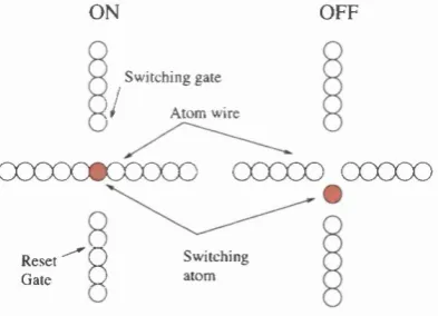
ON OFF
Switching gate
I i
Atom wireoooooeooooo
OOOOO (DOOOO
R e s e t ' ^ P Switching
Gate
Q
atomFigure 1.6: Schematic of an atomic relay (obtained from Goldhaber et al, Proc. IEEE
85, 521, (1997)).
Several theoretical schemes have been proposed to make molecular-scale switches th a t
do not reply on the presence of a STM. Wada [42] proposed a scheme known as the atomic
relay (see Figure 1.6). A mobile atom th at is not firmly attached to the substrate is
present in the junction between four terminals. When the switch is ‘on’, the mobile atom
lies between two terminals, allowing a current to flow between the two terminals. When
the switch is turned ‘off’, an electric field th at passes through the other two terminals
forces the atom to move to one side, thus breaking the connection. Unfortunately, this
switch would require a low operating tem perature, as it would be quite easy to evaporate
mobile atoms off the substrate, for instance by electro-migration induced by the electric
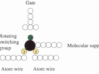
Rather than using the movement of a single atom as a switch, Goldhaber et al [35]
suggested th at a molecule with a rotational group can act as a switch (see Figure 1.7).
When an electric field is applied to the molecule, the switching group would rotate. When
the switch is ‘on’, the functional group th at exists in the gap between the two terminals
has a high conductivity, but when the switch is turned ‘off’ the switching group is rotated
away from the terminals, and a replacement group with a lower conductivity takes its
place.
Gate
Apooco
Rotatinggroup^**^^ ^ ^ B U U U U U Molecular support
ooooo ooooo
Atom wire Atom wire
Figure 1.7: An example of a molecular switch.
We have mentioned the need for nanoscale devices, the physics of these devices and the
various designs that currently exist for these devices. However, for any of these devices
to work we require a method to transm it a net current into and out of these devices. The
obvious solution would seem to be a set of atomic scale interconnects or wires. However
it is an open question whether these wires an d /o r devices need even be fabricated. There
have been theoretical studies th at have outlined the possibility th at one can structure a
material at the atomic scale so th at any switches and wires can be activated or deactivated
by m anipulating the dynamical properties of the system as a whole [50, 51, 52, 53]. These
studies use the atomic scale (subnanometre) structuring of the material so th a t when the
initial one-electron states of the system are acted upon by some outside driving system
(such as a laser), they are driven into final stationary ‘a ttra c to r’ states in such a way
th at a net current has been driven through the m aterial an d /o r the electrical properties
of the material have changed in a measurable way analogous to a set of switches being
thrown. However these studies have (so far) been completely hypothetical.
Another approach th at has been suggested is the quantum cellular autom ata (QCA)
approach. There are two basic approaches, the SET approach [54] and the magnetic
approach [55], in which we have a series of quantum dots which can flip sign (either
adding or subtracting electrons, or changing the sign of the internal magnetic field)
under the influence of an input electric or magnetic field. The SET approach has (at
the moment) limited applications as the operating tem perature is in the range of a few
millikelvins. The magnetic approach operates at room temperature. However we are
interested in electronic transport at a useful operating temperature. Therefore we wish
to concentrate on the seemingly more concrete applications of atomic scale wires. W hat
are our options?
1.3
C an d id ate atom ic scale w ires
There are several different designs for prospective atomic scale wires. These vary from
using molecules, to fabrication using an STM or AFM tip.
1. Molecular wires: These are wires which are formed from molecules. Examples of such wires would include trans-polyacetylene [18, 20, 21, 22, 56, 57, 58, 59], p-
phenylene sulfides [60], fused rigid porphyrin-oligomers [61], the alkanethiols [62],
phthalocyanines [63], the thiophene polyenes [13, 64] and fullerene nanotubes of
carbon [65, 66, 67] and silicon [68].
2. Atomic Nanobridges: These are formed by either an STM tip crashing into the surface and then withdrawing [69, 70], or by electron-beam irradiation [71]. A
short-lived atomic bridge is formed, through which current can flow. However
stress effects tend to destroy these bridges.
3. Dangling Bond Wires: These are formed by using an STM to desorb hydrogen from a silicon surface [72, 73, 74]. The resulting line of dangling bonds are metallic and
can act as wires [75, 76, 77].
4. Zeolitic Chains: These chains are formed by using the cavities of zeolites to con struct atomic scale chains of metals [78, 79], or to construct interlinking chains of
polymers [80].
5. Self Assembled Lines: These lines are formed from the inherent surface properties of the substrate. A material is either deposited on the substrate and self-assembles,
94, 95], gallium on silicon [96] or gold on silic o n (lll) [97, 98, 99, 100, 101, 102].
Alternatively, these structures can be formed by desorbing excess m aterial from
a substrate, such as bismuth from silicon(OOl) [103, 104] or silicon from silicon
carbide(OOl) [105, 106, 107, 108, 109]. Note: The indium and silicon lines can be
formed by either absorption or desorbtion.
As one can see from the above discussion of length scales, one has to be careful about
the nomenclature one uses to describe devices. For example, a nanowire, a quantum
wire and an atomic wire can all mean different things. A nanowire is a wire th a t has
an extent of the order of nanometres (in the literature this can mean anything from one
nanometre to several thousand nanometres). A quantum wire is a wire in which the
electrons display quantum behaviour. Quantum wires can (depending on the m aterial
and the tem perature) be several micrometres in extent. An atomic wire is a wire th at
has an extent of the order of the atomic length scale, i.e. several Â’s. These atomic wires
are necessarily quantum wires, at any accessible tem perature.
Molecular wires are characterised by a sequence of extended repeating structures, or
monomers. The monomers are linked together by tt orbitals. These tt orbitals conjugate
with each other to form a single large tt orbital which is delocalised throughout the
molecule. It is this delocalised tt orbital th at permits electrons to tunnel through the
molecule for a range of electron energy. We can make an analogy with carbon nanotubes,
although in this case the analysis is complicated by the consideration th at a nanotube can
have multiple walls and it is possible to have a series of nanotubes, with each nanotube
surrounded by a larger nanotube (like a Russian Matreski doll). Interactions between
the various nanotubes cause the nanotube to undergo a transition from a metallic to a
semiconducting or insulating phase, and depending on the way a single-walled nanotube is
‘wrapped up’ a single walled nanotube is either metallic or semiconducting [110, 111, 112].
U n dim erised m etallic chain a a bo n d length = a
D im erised m etallic ch ain
bond length = b bond length = c
Figure 1.8: Dimérisation of a molecule.
Some molecules (such as trans-polyacetylene) can undergo a structural transition such
th at a structure where C-C bond lengths are all even transforms to a case where there are
two separate C-C bond lengths, a long one and a short one [18, 59] (see Figure 1.8). This
dimérisation is intimately related to the trans-polyacetylene molecule acting as a one dimensional metal. Although we will not detail the mechanism for such a transition until
the next section, we will define a dimérisation parameter th at represents the magnitude
of this alternation in bond length
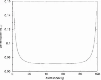
dj - { - i y ( b j j + i - b j j - i ) (1.7)
where 6j,j+i is the length of the bond between atoms j and j + 1. This parameter is far more useful than it would appear, as it enables one to analyze the effect of defects in
an atomic wire in a simple and understandable manner, as a dimerised atomic wire th at
contains no defects has a completely fiat dimérisation curve, and the presence of defects
perturbs this fiat dimérisation curve.
A dangling bond (DB) wire is fabricated by STM desorption of hydrogen on the
hydrogen-terminated surface of silicon, in a Ultra-High-Vacuum system (UHV) (see Fig
ure 1.9). This means th at these systems are not usable in practical atomic-scale devices,
but they can serve as a useful testbed for interesting physical phenomena (such as the
effects of inelastic coupling, see next section). As the hydrogen-silicon bonds are bro
ken by current injection [72] and/or field effect [74] (although probably the former), the
hydrogen atoms evaporate into the vacuum, leaving empty bonds behind. If we depas-
sivate a line either parallel or perpendicular to the (2x1) reconstruction of Si (100), the
empty bonds th at are left are able to overlap. The properties of the specific DB wire
depend on the direction the DB wire runs in, and whether the wire is formed from a row
of single DB’s or a row of pairs of DB’s. However, in all cases the DB wires initially
(before reconstruction occurs) have a finite density of states at the band gap, while the
surrounding hydrogen-terminated surface has a wide band gap [75]. This suggests that
the DB wire is conductive, and th at any electrons th at are injected into the DB wire will
be well confined.
This is an important point th at must be considered in any study of atomic scale wires,
Figure 1.9: A dangling bond wire (image taken from Hitosugi et al, Phys. Rev. Lett. 82, 4034, (1999)).
deposited on a substrate, it depends on the type of force that is holding the molecule
to the substrate. If the molecule is physisorbed (that is there are only weak Van der
Waals type forces holding the molecule in place) then any electrons that are injected into
the molecule will be electronically isolated from the substrate. This is due to the long
residence time of an electron in the bond due to the small bonding energy, as found from
A E A t ~ h. Assuming that forming a Van der Waals bond costs 0.01 eV, an electron resides in the molecule for ~ 10“ ^^s. However, if the molecule is chemisorbed to the
substrate, that is that it is held in place by chemical bonding, then the confinement of
any electrons that are injected into the wire is far from assured. Using the same estimation
approach as before, and assuming that forming a chemical bond costs 1 eV, then a typical
residence time for an electron in the molecule would be of order ~ 10“ ^®s, two orders of
magnitude smaller than the physisorbed case. This also seems to be a potential problem
for self-assembled wires, which are often strongly bonded to the surface and can be stable
at room temperature. One has to look at the charge distribution of states that are close
to the Fermi level and are strongly associated with the wire to see whether they are
constrained to the wire or are free to disperse into the bulk.
We have discussed in general terms how at the nanoscale the behaviour of electrons
can differ from ordinary experience and how we can fabricate devices that can function
at the atomic scale. We have discussed prospective atomic scale wires that could feed
current in and out of these devices (atomic scale electronics). We now need to consider
in more detail what theoretical concepts are useful to study the conductivity of atomic
scale wires and what methods we can use to simulate prospective atomic scale wires.
1.4
Theoretical concepts
At the atomic scale, the properties of materials can differ from their bulk properties.
For instance, it has been reported that a one atomic layer thick film of gold on the
titanium(llO) surface is not metallic but a semiconductor. Another example is a Peierls
distortion [113], an effect which can change the electronic structure of one-dimensional
structures and so is of obvious relevance to atomic scale wires [18, 59, 95].
Let us start off by considering a linear chain of atoms, all equally spaced apart by a
distance a. This means that all multiples of a are lattice vectors, and that the unit cell in reciprocal space is
( 1.8 )
and that the energy as a function of k would be a smooth cosine function if a simple tight-binding model is appropriate (see Figure 1.10).
s
Figure 1.10: Plot of energy as a function of wavevector for a regular undimerised atomic chain.
Now suppose that we displace an atom slightly, with the pattern of each displacement
repeating every rth atom (i.e., every ith atom out of r atoms is moved slightly in the
same direction). The translational symmetry of the linear chain is immediately reduced,
and that instead of having a unit cell containing one atom and having a lattice vector
of a, each unit cell now contains r atoms and has a lattice vector of ra. The cell in reciprocal space is now
< k < —
ra ra (1.9)
r=2 this has the effect of causing vertical breaks to occur at the Fermi surface, caused by the coupling between the filled and empty states. This separates any two eigenvalues
at the Fermi surface which are close to each other (see Figure 1.11). If the pair of
states at the Fermi level are partially occupied in the ideal case (a metal), then following
any distortion one of the states will be displaced downwards in energy and will become
occupied and the state which is displaced upwards in energy will become unoccupied.
The metal will become a semiconductor.
Figure 1.11: Plot of energy as a function of wavevector for a dimerised semimetallic chain.
It follows that for a one-dimensional metal with a partly filled band a regular chain
structure will never become stable, as it is always possible to find a distortion with a
suitable value of r for which a band gap will open up at or near the edge of the Fermi
distribution. To maximise the gain of energy, and hence the distortion, r has to be small
number, unless there are other metallic bands or strong correlation effects. Neglecting
these factors the favourable case is that in which the Fermi distribution ends at A: =
7r /2a. This means that there is one electron per atom, including spin. This means that
r = 2, and that there is a regular bond alternation, or dimérisation, which is observed to
occur in (for example) polyacetylene. The Peierls distortion is an electronic effect that is
associated with the top of the valence band/bottom of the conduction band, and which
can be represented as a sum of different phonon modes. Thus if we inject an electron
(or hole) into the system we would change the physical structure of the system as this
would change the electronic structure at the bottom of the conduction band (top of the
valence band). We can thus say that the Peierls distortion increases the magnitude of
electron-phonon coupling.
If we just included electronic effects, then it would seem that the way to maximise
the gain in energy would be to have two vastly different bonds, one with a very long
(or infinite) bond length, the other with a very small (or zero) bond length. We need to
balance the gain in electronic energy with the loss in elastic energy, so that the equilibrium
deformation u q is given by the roots of
, ( ^ /e le c tr o n ic "b ^ e l a s t i c ) — 0
-duo (1. 10)
There are two values of uq. Thus there are in extremis two cases [114].
i
Figure 1.12: Twofold degeneracy of energy.
s
u
_0(i*«orton from
•«»)
Figure 1.13: Near-twofold degeneracy of energy.
I
Figure 1.14: Near-onefold degeneracy of energy.
Firstly if the two values are exactly equal then the ground state of the one-dimensional
metal is twofold degenerate (see Figure 1.12). That is that we can have two identical
bond alternation patterns, 1= 2 -3 = 4 -5 = 6 -7 = 8 -9 = 1 0 , and 1-2= 3-4= 5-6= 7-8= 9-10, where
- signifies a long bond and a = a signifies a short bond. This doubly degenerate ground
state supports nonlinear excitations which can act as moving domain walls separating
different phases. That is, in the chain it is possible to have two phases A (-l-uo) and B(-
Each phase has its own dimérisation parameter, one positive, the other negative. Where
the two phases meet, the dimérisation will change sign (see Figure 1.15). This can be
represented as a-a=a-a=a-X-b=b-b=b-b, where X is the discontinuity (see Figure 1.16).
:
Figure 1.15: The dimérisation profile of a soliton.
Perfectly Dimerised chain
Chain with Soliton defect
Figure 1.16: Structure of a soliton in a chain.
In the limit of a long chain, a soliton corresponds to a phonon field configuration that
approaches the B phase as N-> oo, approaches the A phase as N—> —oo, and minimises
the total energy. The width of a soliton ( depends on the competition of two effects, the
electronic energy and the elastic energy per site. If the soliton is very narrow, then the
sudden change in dn from the - u q to +uq state (at n=0 say) will cause the electronic energy to be large because of the uncertainty principle. If however, dn changes very slowly from the - u q state to the +uo state, there will be a large region surrounding n=0
where the elastic energy is greatly reduced again raising the energy [18]. ( is the width
of the soliton that minimises the the total energy. If ( is large compared to the average
lattice spacing a, then as the soliton moves relative to the lattice the variation of the
energy is small. This large soliton width also means that the soliton has an extremely
small effective mass, of the order of an electron mass rather than an ionic mass. This
means that if an electron (or hole) is injected into the chain then it would be energetically
preferable for the charge to be transported along the chain as a soliton rather than as
a free electron as the effective mass is so much smaller. Note th at as a moving soliton
changes A-phase material to B-phase material and vice versa, th at injected solitons can
only be created or destroyed in pairs.
The presence of a soliton in the chain also affects the electronic spectrum. For each
widely separated soliton there exists a normalised single-electron state of zero energy in
the gap centre which can accommodate zero, one or two electrons and th at has an extent
of order (. For a neutral soliton this state is singly occupied by an electron. Therefore
we have a case where the neutral soliton has a spin of We would expect a spin ^
particle to have a charge of ±e. Conversely when the soliton is charged the occupancy
of the band gap state is 0 or 2 electrons, which means th at it is carrying ± e and has a
spin of zero. This means th at the soliton has reversed spin-charge relations.
Solitons have been observed to form in two ways, either by doping or by initial chain
conditions. It has been observed th at doping trans-polyacetylene with sodium ions leads
to the spontaneous creations of solitons in the chain. Solitons are also formed naturally if
the polyaoetylene chain consists of an odd number of monomers. This would mean that
one end of the chain would end in a single bond and the other end of the chain would
end in a double bond. Polyacetylene would rather have a double bond at both ends of
the chain, so a soliton is formed at one end of the chain and travels to the centre. Thus
for odd numbered chains a soliton is formed in the ground state. It is possible to form a
soliton-antisoliton pair S S from an electron-hole pair. Functionally this pair resembles a
polaron which is explained below.
For the more general case th at the two values of uq are nondegenerate (see Figures
1.13 and 1.14), the dominant charge carriers and excitations are polarons. A polaron
is an electron-phonon excitation, in which the interaction of the electron with phonons
allows the electron to be surrounded by a strain field and the movement of the electron
is matched by the movement of the strain field. This has the effect of increasing the
apparent mass of the electron [116]. Compared to the solitons considered previously,
the formation of a polaron in the chain does not change the value of the dimérisation
far away from the defect. The presence of a polaron merely induces a reduction in the
local dimérisation (see Figure 1.17). There thus exist the following symmetries for the
dimérisation d of the chain as a function of x when the defect (polaron or soliton) is at