Frequency Selective Surface with Improvised Ring-Resonator
for Flexible Design
Gargi Saha1, Chandrakanta Kumar2, *, and Venkataraman V. Srinivasan2
Abstract—Ring resonators are very commonly used for the design of frequency selective surfaces (FSSs). But, for some particular design, the spacing between the resonators becomes very small. So it leaves no space to shift the reflection band towards the lower side of the spectrum. It also becomes very difficult to realize large PCBs. In this paper, an improvised design of the ring resonator using stubs is reported. This provides the designer with some flexibility. Two different configurations using this concept have been fabricated. Measured results are compared with the configuration using conventional ring resonators. These results indicate good performance with tune-ability in the response without major change in the design or in the substrate.
1. INTRODUCTION
Frequency selective surfaces (FSSs) find specialized application in the design of spacecraft antennas meant for deep-space missions. As the resources in a spacecraft become scarce, the antenna designers are compelled to explore the possibility of using the same antenna aperture for operations in multiple frequency bands. The frequency selective property of FSS of being totally reflective at a designed band and almost transparent in another, provides the designer with the opportunity to combine the energy radiated from different feed antennas onto the aperture of a single reflector antenna. Thus a compact antenna system can be realized leading to large savings in spacecraft mass.
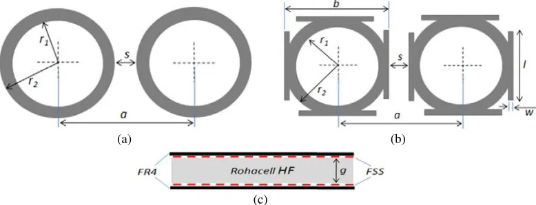
(a)
(c)
(b)
Figure 1. Schematic diagram of the FSSs under investigation: (a) conventional ring element, (b) ring element with stubs, (c) cross sectional view of the dual layer FSS.
Received 19 January 2015, Accepted 27 February 2015, Scheduled 8 March 2015
* Corresponding author: Chandrakanta Kumar ([email protected]).
1 University of Burdwan, India; and was working at Communication Systems Group, ISRO Satellite Centre, India. 2Communications
The FSSs are more interesting because, their frequency selective nature is not due to any material property but, due to some metallic patterns etched onto the sheet of a dielectric material. To be more precise, FSS per se does not need a substrate for its operation but for holding the repetitive metallic patterns together in the form of an array. There are different designs of the individual elements as well as of the array which are of particular interest of a designer.
The design aspects of FSS elements have been investigated by many researchers. Few of them are listed in [1–7] and most of the research works till the year 2000 have been discussed in [8]. Different configurations have been categorized under four groups [8] according to the topology of their geometry. Each of the elements has their specific advantages and application areas. Such is the case with the ring element [4, 6–9]. It provides more than 25% reflection bandwidth and maintains good polarization purity [4]. Sensitivity of the performance with varying angle of incidence of the electromagnetic (EM) wave is low for ring elements. Analysis of any general configuration of FSSs is discussed in [5] and that for the ring geometries is discussed in [10, 11]. Concentric ring resonators can be used for achieving multiband operations [7]. Active and/or lumped components can also be embedded within the ring to operate them at a different state or to realize a compact configuration [12, 13]. The design parameters of FSS using ring as elements are shown in Fig. 1(a). The detail of different aspects of their design can be found in [6].
While working with the FSS using ring elements, it is found that the geometry of some particular design do not offer any flexibility to lower the operating frequency of the reflection band. This is mainly due to the fact that it needs bigger rings which may not be possible to be accommodated within the space available.
Table 1. Substrate: FR-4: Thickness = 0.75 mm, εr = 4.3, and tan(δ) = 0.013. ROHACELL HF: Thickness,g= 9 mm, εr = 1.04 and tan(δ) = 0.0017. Metallization Thickness = 0.0175 mm.
config. a (mm)
element parameters (mm) stub param. (mm)
first layer second layer
l w
r1 r2 b s r1 r2 b s
ring 9 4.1 4.3 - - - 0.4 3.6 4.3 - - - 0.4 - - -
-stub-1 9 4.1 4.3 8.4 0.6 3.6 4.3 8.4 0.6 4 0.3
stub-2 9 4.1 4.3 8.4 0.6 3.6 4.3 8.4 0.6 5 0.3
In this paper, an improvised FSS design involving ring as the basic element is presented. Four rectangular stubs of dimension (l×w) are attached to the rings as shown in Fig. 1(b). With this configuration the designer can have some flexibility in lowering the frequency of operation. This also allows varying the spacing between the rings ‘s’ which is very important with respect to the fabrication of the printed surfaces.
2. NOMINAL DESIGN USING RING RESONATORS
The present design is targeted for application in an antenna that needs to cover the deep space communication at S- and X-bands. Keeping some margin for the design the pass-band for the FSS is taken as 2–2.7 GHz and the reflect band as 7–9 GHz. This is a very common requirement and can be met using nominal configuration of ring elements [6].
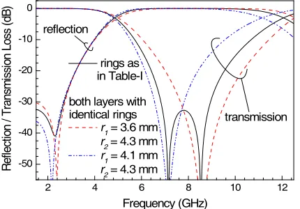
2 4 6 8 10 12 -50 -40 -30 -20 -10 0 reflection transmission R e flec tion / T rans m is si on Los s ( d B ) Frequency (GHz) rings as in Table-I
both layers with identical rings
r1 = 3.6 mm r2 = 4.3 mm
r1 = 4.1 mm r2 = 4.3 mm
Figure 2. Simulated response of dual layer FSSs with different rings in the two layers as in Table 1 and with identical rings in both the layers.
2 4 6 8 10 12
-50 -40 -30 -20 -10 0 reflection transmission R e fle ct io n / T ra n sm issi o n L o ss ( d B ) Frequency (GHz)
a = 9 mm 8.7 mm 9.5 mm
Figure 3. Simulated response of dual layer FSS with conventional ring elements for varying array spacing, a. Other parameters: in 1st row of Table 1.
in this situation is not possible because the available gap between the rings,s, is already very small. So only the inner radius (r1) of the rings is increased such that the effective radius of the ring which lies betweenr1 andr2 is increased. This leads to the increase in the perimeter of the ring which lowers the resonant frequency. But, this also reduces the thickness of the ring (r2−r1) which makes it a narrow band resonator. The simulated response of this configuration is also shown in Fig. 2. These results corroborate the observations made above. So, these two types of rings with their staggered resonant frequency are combined such that the required wide frequency band can be covered.
3. LIMITATION OF THE DESIGN USING RING
This design using conventional ring resonators meets the present requirements and can be used as such. But, a critical look at the design reveals that the designer has to work in a closed loop with contradicting requirements of the parametersa; the periodicity of the array andr2; the outer radius of the ring. Value of a is determined by the highest frequency of operation and the angle of incidence of the EM wave, whereas,r2 is related to the lower frequency side of the reflection band. Their values are geometrically related as r2 ≤ (a−s)/2. Thus for a given value of a, the choice of value of r2 gets restricted to a maximum allowable limit. Hence, the lower range of operation for which the rings can be used also get restricted. The value of s is already very low, so the radius of the rings cannot be increased without increasing the value ofa. But, it can be seen from the Fig. 3 that even any small increase in the value of
ashifts the reflection frequency band towards the higher side of the spectrum. The spacings between the rings also cannot be reduced beyond a certain limit for practical limitations in fabrication of large PCBs using chemical etching technique. In the present design the value ofsis 0.4 mm which is already very close to the limit for a common PCB facility for a large size of board. This is more critical for the design operating at multiple and higher frequencies where value ofais reduced further.
So the only option seems to be left is to use a material with higher thickness or relative permittivity. But, it tends to increase insertion loss and excite surface wave. This also adds to the cost and mass of the hardware.
4. STUBBED RING: AN IMPROVISED DESIGN
2 4 6 8 10 12 -50 -40 -30 -20 -10 0 reflection transmission R e flec tion / T rans m is si on Los s ( d B ) Frequency (GHz) only ring with stub
l = 4 mm 5 mm 6 mm
Figure 4. Simulated response (TE00 mode) of dual layer FSS with conventional rings and rings integrated with stubs of varying length, l. Other parameters: in Table 1.
2 4 6 8 10 12
-50 -40 -30 -20 -10 0 transmission reflection
s = 0.4 mm
s = 0.6 mm
l = 5 mm
R ef le ct io n / T ra nsm issi on L oss ( dB ) Frequency (GHz) only ring
l = 5 mm
Figure 5. Comparison of the simulated response (TE00mode) of dual layer FSS using ring element and new-element with 5 mm long stub for varying gap between the elements, s. Other parameters: in Table 1.
the currents in the ring is altered. As a result the electrical length of the rings is also changed. This concept has been implemented in this design.
As shown in Fig. 1(b), rectangular stubs of dimension l×w are attached to the ring resonators. Four of them are attached to a ring to maintain the symmetry in the square array in the present design. The location of these stubs is dependent on s. If enough space is available then the stubs can start tangentially to the outer edge of the ring, otherwise, as in the present case, stubs can move closer to the center of the ring such that a part of the stub overlaps with the ring. The parameterbin Fig. 1(b) controls the location of the stubs. Ifbbecomes less than (2×r2), then the projection of the ring beyond the stubs may also be trimmed which increases the spacing, s. Three parameters namely b,l andw of the stub can be used to control the response of the FSS to some extent without altering the ring or the substrate parameters.
Simulated response of the configurations in Table 1 for varying length of the stub is shown in Fig. 4. It can be seen that with increased stub length the resonant frequency is lowered. However, the corresponding reflected power in the pass-band is also increased slightly which is more sensitive for the orthogonal, i.e., TM00 mode which will be addressed later. Considering this aspect it is found that for the present configuration a stub of length 5 mm can be used without much degradation in performance the corresponding shift in the frequency is about 600 MHz which is about 8% in terms of the fractional bandwidth.
In Fig. 4, the spacing between the resonator sis kept 0.6 mm by trimming the projection beyond the stubs as discussed above. This was to relax the PCB fabrication constraints. It can be seen from Fig. 5 that if this value was kept at 0.4 mm as that was in ring DGS, even more shift in frequency could have been achieved. The corresponding shift in frequency with respect to the conventional ring resonator is more than 1 GHz. However, degradation in reflection property in the passband is slightly more in this case. So with s = 0.4 mm a lower value of l could have been used. This provides the flexibility in the design.
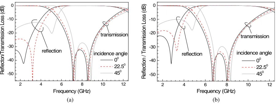
2 4 6 8 10 12 -50 -40 -30 -20 -10 0 reflection transmission incidence angle R e flec to n/ T rans m is si on Los s ( d B ) Frequency (GHz) 00 22.50 450
2 4 6 8 10 12
-50 -40 -30 -20 -10 0 reflection transmission incidence angle R e fle ctio n / T ra n sm is si o n L o ss ( d B ) Frequency (GHz) 00 22.50 450 (a) (b)
Figure 6. Simulated response (TM00 mode) of dual layer FSS for varying angle of incidence, (a) ring element, (b) ring integrated with stub (l= 5 mm); Other parameters: in Table 1.
incidence. Considerable reduction in reflectivity for the angles of incidence of 0◦ and 22.5◦ is observed compared to the FSS with conventional rings. But, still minimum of −19 dB of reflection coefficient is observed for these angles. However, for the incidence angles of 45◦ where the reflectivity was as such low with conventional ring, is reduced only by 2 dB. But, these variations cause hardly any significant change in the primary property at S-band, i.e., insertion loss of the FSS. Additionally, for any practical application, the power from the feed at a wide angle which illuminates the edge of the reflector is also less. Considering these aspects and the relative performance over the entire band, the design with stubs of reasonable length is still found to be acceptable.
5. MEASUREMENTS AND RESULTS
Three configurations of FSSs as mentioned in Table 1 were realized for experimental verification. Rectangular panels of dimension 430 mm×535 mm incorporating 2773 resonators on each surface were fabricated using standard PCB fabrication technique using chemical etching. Commercially available, 0.75 mm thick FR4 substrate with relative permittivity of 4.3, and tan(δ) = 0.013 has been used. Two panels corresponding to a particular configuration were aligned face-to-face using alignment holes. ROHACELL HF foam with relative permittivity 1.04 and tan(δ) = 0.0017 has been placed between them in sandwich configuration. Photographs of the fabricated panels and one of the assembled FSS are shown in Fig. 7.
Both the surfaces of the FSS, realized using PCB fabrication technique have very high accuracy with respect to the dimensions of the rings and stub. However, there may be some deviation in the alignment of both the surfaces as it has been done manually. Effect of this has been studied using simulation results which indicate that a lateral mismatch of 0.5 mm in both the axes also does not have much effect. However, the performance is sensitive to the gap g between the two layers. Due to an increase of 0.5 mm in g the reflection coefficient at S-band shows a shift towards the lower side of frequency by about 150 MHz. The shift occurs towards higher side for reduction in g. But, the transmission property is not so sensitive to these changes. However, special care was taken by using spacers of exact thickness during assembly to maintain the spacing. The alignment between the two layers was ensured using multiple alignment pins.
(d)
(a) (b) (c)
Figure 7. Photographs of the fabricated FSSs; zoomed view of the elements of both the surfaces shown side by side, (a) ring elements, (b) with 4 mm stub, (c) with 5 mm stub, (d) assembled view of the FSS with ring elements: Parameters: as in Table 1.
(a)
(c) (b)
(b) (c) (a)
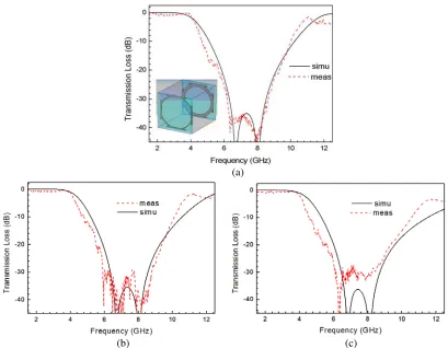
Figure 9. Measured and simulated frequency response of the transmission loss of dual layer FSS with the resonator integrated with 5 mm stub. Parameters: in Table 1; angle of incidence: (a) 0◦, (b) 20◦, (c) 45◦.
(a) (b)
Figure 10. Frequency response of the transmission loss for 0◦ angle of incidence of dual layer FSS with three different elements as in Table 1. (a) Measured, (b) simulated.
Similar set of results for the FSS using resonator with 5 mm stubs is shown in Fig. 9. Reasonably good match between the measured and simulated results are observed. As per the design the shift in frequency is evident in the measured results also. The stub moves the reflection band towards lower side of the frequency by about 600 MHz.
The transmission property of all the three configuration as in Table 1 is shown in Fig. 10. The corresponding simulated results are also incorporated there showing good matching with the measured results. Relative shift in the resonant frequency with the introduction of the stub of varying length is evident from these plots.
6. CONCLUSION
The design of FSS involving improvised ring resonators integrated with stubs is presented. This provides the designer with additional control to shift the resonant frequency towards the lower side of the spectrum without changing the basic design or the substrate parameters. Different parameters of the stubs can be varied to achieve the required shift. In another sense it provides some sort of tuning provision in the design. The disturbance in the rotational symmetry of the ring resonator shows slight degradation in the performance. This is manifested as small variation on the reflection property of the FSS in the pass-band for one particular mode of incident wave. These variations are practically very negligible. This design can also be used for reducing the size of the ring resonators for design at a particular band.
REFERENCES
1. Lee, S. W., “Scattering by dielectric-loaded screen,”IEEE Trans. Antennas Propag., Vol. 19, No. 5, 656–665, 1971.
2. Montgomery, J. P., “Scattering by an infinite periodic array of thin conductors on a dielectric sheet,” IEEE Trans. Antennas Propag., Vol. 23, No. 1, 70–75, 1975.
3. Agrawal, V. D. and W. A. Imbriale, “Design of a Cassegrain sub-reflector,”IEEE Trans. Antennas Propag., Vol. 27, No. 4, 466–473, Jul. 1979.
4. Parker, E. A. and S. M. A. Hamdy, “Rings as elements for frequency selective surface,” Electron. Lett., Vol. 17, No. 17, 612–614, 1981.
5. Mittra, R., C. H. Chan, and T. A. Cwik, “Techniques for analyzing frequency selective surfaces-a review,”Proceedings of IEEE, Vol. 76, No. 12, 1593–1615, Dec. 1988.
6. Huang, J., T. K. Wu, and S. W. Lee, “Tri-band frequency selective surface with circular ring element,” IEEE Trans. Antennas Propag., Vol. 42, No. 2, 166–174, Feb. 1994.
7. Wu, T. K. and S. W. Lee, “Multiband frequency-selective surface with multiring patch elements,” IEEE Trans. Antennas Propag., Vol. 42, No. 11, 1484–1490, Nov. 1994.
8. Munk, B. A.,Frequency Selective Surfaces: Theory and Design, John Wiley & Sons, 2000.
9. Baisakhiya, S., R. Sivasamy, M. Kanagasabai, and S. Periaswamy, “Novel compact UWB frequency selective surface for angular and polarization independent operation,”Progress In Electromagnetics Research Letters, Vol. 40, 71–79, 2013.
10. Yao, X., M. Bai, and J. Miao, “Equivalent circuit method for analyzing frequency selective surface with ring patch in oblique angles of incidence,”IEEE Antennas and Wireless Propagation Letters, Vol. 10, 820–823, 2011.
11. Orta, R., P. Savi, and R. Tascone, “Multiple frequency-selective surfaces consisting of ring patches,” Electromagnetics, Vol. 15, No. 4, 417–426, 1995.
12. Taylor, P. S., E. A. Parker, and J. C. Batchelor, “An active annular ring frequency selective surface,” IEEE Trans. Antennas Propag., Vol. 59, No. 9, 3265–3271, Sept. 2011.
13. Xu, R. R., H. C. Zhao, Z. Y. Zong, and W. Wu, “Dual-band capacitive loaded frequency selective surfaces with close band spacing,” IEEE Microwave and Wireless Components Letters, Vol. 18, No. 12, 782–784, Dec. 2008.