EFFICIENT APPROACH FOR DESIGNING LOW
POWER REVERSIBLE
DECODER/ENCODER WITH
LOW QUANTUM COST
Sweta Mann
1, RitJain
2 1,2Department of Electronics and Communication Engineering, LNCT Bhopal (M.P), (India)
ABSTRACT
This paper presents realization of reversible decoder/encoder which can provide low quantum cost values to
obtain energy effiecient logic design. Proposed design of reversible decoder is compared with the existing
counterpart and performance anaylsis is done in terms of quantum costmainly In this paper, an approach for
designing is carried on a novel design of 2:4 decoders, which has been used to build a 3:8 decoder and 8:3
decoder, futher design can be extended to n:2n decoders or vice versa. The reversible logic circuits are
deginedand simulated. The simulation results are obtained using Xilinx ISE version 14.1.
Keywords –Reversible Decoder, Reversible Logic, Quantum Cost, , Reversible Encoder, Low Power
I. INTRODUCTION
In today’s era, reversibility has become essential part of digital world to make digital circuits more effiecient. Reversible logic performs all operations in an invertible manner that marks a promising new direction. As compare with traditional logic, all comupations can be reverted . Power dissipation and heat generation is a serious problem for today’s computer chips. Landauer proved [1] that using traditional (irreversible) logic gates always lead to energy dissipation. Whearas, reversibility in computing [2]-[3]signifies that no information about the computational states can ever be lost, so it can be recovered at any earlier stage by computing backwards the results.
Heat generated due to the loss of one bit of information during computation is about KTln2 in joules. C.H. Bennett [4], obsereved that we can avoid KTln2 joules amount of anergy dissipation by designing or constructing circuit using reversible logic gate, interest in this field is motivated by its applications in severeal technologies involving low voltages and low power. Few of its application area include CMOS low power design, quantum computing, network security, digital signal and image processing, optical electronics and nanotechnology.
1.1 Quantu Cost
1.2 Garbage OutputThe output of the reversible gate that is not used as a input to other gates is called the garbage output.
1.3 Reversible logic
Reversible circuits [5] are those circuits, which have one-to-one mapping between input and output vectors. A circuit/gate is said to be reversible if the input vector can be uniquely recovered from the output vectors and there is a one-to-one correspondence in order to preserve information during computation.
1.4 Revesible Decoder/encoder
A decoder is a device which does the reverse operation of an encoder, undoing the encoding so that the original information can be retrieved. The same method can be used to encode is usually just reversed in order to decode. Reversible decoder/encoder combinational circuits are constructed using reversible logic only. In digital design, decoder find extensive usage – in control unitfor addressing a particular location for read/write operation in memory cells, in I/O processor, in Analog to Digital and Digital to Analog Converters, which are used in various different stage of a communication system.
II.REVERSIBLE LOGIC GATES
In his section, we have presentedfew reversible logic gates, which are used for constructing the combinational circuits design presented in this paper.
2.1 Fredkin Gate (FRG)
Fredkin Gate [6] is a 3x3 reversible logic gate shown in Fig. 1 with 3 inputs and 3 outputs. The quantum cost of the Fredkin Gate is 5. The Fredkin gate maps (A, B, C) to (P = A, Q = A’B+AC, R = AB+A’C) where A, B, C are the inputs and P, Q, R are the outputs respectively. A Fredkin gate can also work as 2:1 MUX,because it is ready to swap its 2 different inputs depending on the value of its first input.
Figure 1: Fredkin Gate
2.2 R Gate
R gate is 3x3 reversible gate whose block diagram is shown in Fig.2 having inputs (A, B, C) and outputs (P =A, Q =AB and R = A’B+AC)
2.3 HL Gate
HLgate is a 4x4 reversible gate [7], namely HL gate is shown in Fig. 3. Quantum cost of HL gate is seven. HL
gate can also work as 2:4 decoders. The 2-to-4 decoder requires only one HL gate without any garbage output.
Figure 3: HL gate (2-to-4decoder)
III. DESIGN AND OPERATION OF REVERSIBLE DECODER
A decoder is a fundamental bulding block in many computing systems which can take the form of a multiple- input, multiple-output logic circuit that converts coded inputs into coded outputs, There are several designs of reversible decoders in literature. To the best of our knowledge, the designs [8] fromis chosen for comparision. Inthis paper, 2:4 decoders using new reversible gate, namely HL gate. It has improved quantum cost while design is extended to reversible 3-to-8 decoder [9] can be designed using one 2 to4 reversible decoder was greater as in compare to previous designs in terms of quantum cost.
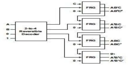
A reversible 3-to-8 decoder can be designed using HL gate which acts as 2-to-4 reversible decoder and four R gates shown in Fig. 5. Having bettter performance results as compared to existing counterpart as shown in Fig. 4. Quantum cost of 3-to-8 reverisble decoder using R gate is 23 awhen compaerd by using FRG gate which is about 27.
Figure 4: Previously proposed 3:8 reversible decoder
3.1 Reversible Encoder
Due to logical reversiblity of our proposed design, it can also be configured to operate in reverse manner as a reversible encoder[10]. Simply reflecting the reversible decoder design horizontly (Fig. 5) yields a gate that can reversibly implement a 8-to-3 encoder. Reversible 8-to-3 encoder design assumes-like traditional encoders-that exactly one of its eight inputs will have an input value of logical 1 at any time. When functioning this way as areversible 8-to-3 encoder wih same quantum cost as decoder but number of garbage outputs will increase as compared to decoder in case of reversible encoder.
IV.SIMULATION RESULTS AND DISCUSSION
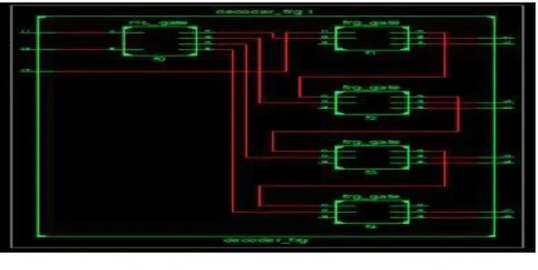
The software used for viewing RTL schematic of the decoder circuit is Xilinx ISE 14.1 on spartan device 3 family and Xilinx simulator is used for checking the output waveforms. Fig. 6 and Fig. 7shows the RTL of 3_to
8 decoder using R gates and Using FRG gates respectively. RTL view basically provides information regarding the hardware implementation of then the circuit. Each box represent R gate and total of four R gates are used in
3:8 decoder.
Figure 6: RTL view of 3_to_8 reversible decoder using R gates
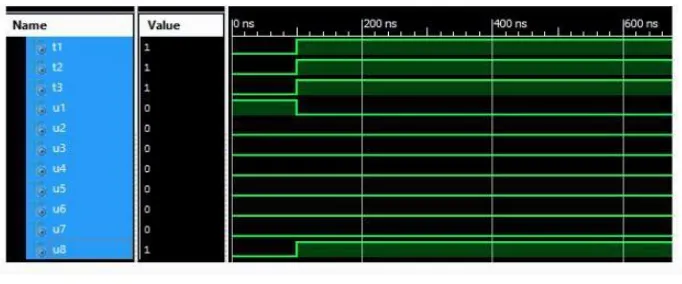
Output waveforms of proposed 3:8 decoderis shown in Fig. 8 using R gate. Here t1, t2 and t3 are three inputs and u1 to u8 are the corresponding outputs.And Fig. 9 represent the ouput waveform of reversible decoder using FRG gates, where u1 to u8 represents the inputs and t1, t2 and t3 are three ouputs respectively.
Figure 8: Output waveform for 3:8 reversible decoder using R Gate
Figure 9: Output waveform for 3:8reversible decoder using FRG Gates
We can see that in the RTL view of reversible decoder each logic gate have an equal number of inputs anad outputs, means each input can be reversibly obtained from the outputs. Hence ideally no power dissipation takes place [2]. Also each output is used only once in case of reversible logic.Results are compared with best existing design [8] for reversible decoder using FRG gate with proposed design using R gates and tabulated in TABLE 1 as shown below.
Table-1: Comparison of existing and improved design
Design Reversible
logic used
Quantum
Cost
Improvement
3:8
Decoder
FRG gate 27 14.81%
R gate 23
:3
Encoder
FRG Gate 27 29.62%
V. CONCLUSION
Decoderare the collection of logic gates fixed up in a specific way such that, for an input combination, all outputs terms are low except one. In this paper we have presented a novel technique for designing a 8 to 3 encoder using reversible logic has been discussed. We have seen by using reversible logic there is a powerconsumption by using this technique as comparerd to conventional decoders. While using R gates reversible circuit design having better performance than FRG gates and shows improvement of 14.81% for decoderin terms of quantum cost. Also further work can be done by to find optimal solution, which produces the minimum Garbage outputs, constant input, number of gate count and area.
REFRENCES
[1
] R. Landauer, Irreversibility and heat generation in the computing process,IBM Journal of Research and Development, vol. 5, 1961, pp. 183-191.[2] Nusrat Jahan Lisa, Hafiz Md. Hasan Babu, A Compact Realization of a Reversible Quantum n-to-2n Decoder, 4th IEEE international conference, University of Dhaka, Bangladesh, 2013.
[3] L. Jamal, M. Shamsujjoha, and H. M. Hasan Babu, Design of optimal reversible carry look-ahead adder with optimal garbage and quantum cost, International Journal of Engineering and Technology, vol. 2, 2012, pp. 44–50, 2012.
[4] C. H. Bennett, Logical reversibility of computations, IBM Journal ofResearch and Development, vol. 17, 1973, pp. 525-532.
[5] Perkowski M. and P. Kerntopf, - Reversible logic. Invited tutorial, Proc. EURO_MICRO, Sept 2001, Warsaw, Poland.
[6] Raghava Garipelly, P. Madhu Kiran, A. Santhosh Kumar, A Review on Reversible Logic Gates and their Implementation, International Journal of Emerging Technology and Advanced Engineering, Vol. 3, March 2013.
[7] Lafifa Jamal, Md. Masbaul Alam, Hafiz Md. Hasan Babu, An efficient approach to design a reversible control unit of a processor, Informatics and Systems, Vol.3, 2013, pp.286-294.
[8] Lafifa Jamal and Hafiz Md. Hasan Babu, Design and Implementation of a Reversible Central Processing Unit, IEEE Computer Society Annual Symposium on VLSI, Dhaka, Bangladesh, 2015 IEEE.
[9] Sweta Mann and Rita Jain, Design of 3:8 Reversible Decoder using R gate, International Journal of Electrical and Electronics Engineering, Chandigarh, India, June 2017
[10] Michael Nachtigal, and Nagarajan Ranganathan, Design and Analysis of a Novel Reversible Encoder/Decoder, 11th IEEE International Conference on Nanotechnology Portland Marriott, Portland, Oregon, USA, 2011.