Fabrication of Large Mechanically Flexible Multi-Layered PDMS
Fabrication of Large Mechanically Flexible Multi-Layered PDMS
Optical Devices
Optical Devices
Robert S. Green
The University of Western Ontario
Supervisor
Dr. George K. Knopf
The University of Western Ontario
Graduate Program in Mechanical and Materials Engineering
A thesis submitted in partial fulfillment of the requirements for the degree in Master of Engineering Science
© Robert S. Green 2016
Follow this and additional works at: https://ir.lib.uwo.ca/etd
Part of the Manufacturing Commons, Other Mechanical Engineering Commons, Polymer and Organic Materials Commons, and the Semiconductor and Optical Materials Commons
Recommended Citation Recommended Citation
Green, Robert S., "Fabrication of Large Mechanically Flexible Multi-Layered PDMS Optical Devices" (2016). Electronic Thesis and Dissertation Repository. 4147.
https://ir.lib.uwo.ca/etd/4147
This Dissertation/Thesis is brought to you for free and open access by Scholarship@Western. It has been accepted for inclusion in Electronic Thesis and Dissertation Repository by an authorized administrator of
Mechanically flexible large area polydimethylsiloxane (PDMS) optical devices are fabricated
using soft-lithography techniques based on replica moulding. These non-rigid optical devices
can be designed as sheets to act as either light concentrators (collectors) or diffusers (illumina-tors) based on the position and geometry of micro-optical structures (MOSs) embedded within
the sheet or imprinted on its surface. The active surface area of the device can range from
less than a sq. cm to several sq. m. The performance of the large area optical device is a function of the location and geometry of micro-optical structures, thickness and shape of the
flexible waveguide, core and cladding material (ie. refractive indices), and the wavelength of
the incident light source. A centrifugal casting technique that simultaneously de-gasses and
fills a patterned, thin mould cavity is introduced as the backbone to the proposed fabrication
methodology. Combined with the ability to control the refractive index of PDMS and a partial
curing technique that bonds subsequent layers, a bottom-up layer-by-layer fabrication process
is proposed and described in detail.
Keywords:Flexible large area optical device, soft lithography, polydimethylsiloxane (PDMS),
polymethylmethacrylate (PMMA), micro-machining, micro-optical features, centrifugal
cast-ing, partial curing
• General Hyperlinking: The table of contents and each figure, table and equation
refer-ence in the text has been hyperlinked inredto its corresponding element. Clicking one
of these red reference links will jump you to its location in the document.
• Citation Look-up:Each citation in the text has also been hyperlinked, but inblueto its
corresponding location in the bibliography. Additionally, digital object identifier (DOI)
links have been added in the bibliography inmagenta. Clicking these links will open a page in your default web browser where the cited paper was found.
• Abbreviations & Nomenclature: Instances that appear in paragraph text have a small
hover tool-tip added to them. If you’ve forgotten what a symbol or abbreviation means
while reading, simply hover over it with your mouse to see its long-form. Try it: PDMS.
Note: Hover tool-tips may only work on higher-level PDF readers, such as Adobe Acrobat
Reader. Other readers may implement this feature at a later date.
Obtaining a Master’s degree in Engineering Science has been no easy task. Such a feat might
not have been possible without the much appreciated help of others. I would first like to thank
my family and friends for their constant support and encouragement. Without them, a white
surrender flag may have been planted after the many fails from the initial mould iterations
summarized in appendixB.
My supervisor Prof. George K. Knopf and co-supervisor Dr. Bordatchev have been very understanding and have overall been two inspiring role models always offering help, advice, and encouragement. I appreciate the chance they have given me to come up with a solution
to such a complex and interesting fabrication-based problem; I could not have done it without
them. I must also thank my project partner, Chlo¨e Nicholson-Smith, who worked on the
sim-ulation side of illuminator and collector design. Not only did she supply me with functional
design parameters for my prototypes, but she also supplied me with a new ”bright side” to
every failed fabrication experiment I encountered to keep me going; for that I am very grateful.
My appreciation also goes out to Western Universities’ Machine Services where many
tal-ented machinists allowed me to pick their brains for fabrication-related advice and interesting
techniques for fabricating my moulds. Special appreciation goes out to Chris Vandelaar for his after-hours help on the design and fabrication of my final aluminium mould. Without Chris,
I’d be stuck using acrylic moulds which don’t allow for enough clamping force and expand far
too much when heated. Finally, I would like to thank one particular friend, Ben Hamilton, for
allowing me to bombard him with constant CNC-related questions throughout my two years of
research; I hope I didn’t distract you too much!
Acknowledgements iii
List of Figures viii
List of Tables x
List of Appendices xi
List of Abbreviations and Nomenclature xii
1 Introduction 1
1.1 The Problem . . . 1
1.2 Applications of Large Area Flexible Optical Devices . . . 2
1.3 Research Motivation . . . 3
1.4 Objectives of Research . . . 3
1.5 Overview of the Thesis . . . 4
2 Literature Review of Large Area Flexible Optical Devices 6 2.1 Introduction . . . 6
2.2 Properties of Light . . . 7
2.2.1 How Light is Created . . . 8
2.2.2 Absorption, Reflection & Transmission . . . 9
2.2.3 Light Propagation . . . 11
2.2.4 The Law of Refraction and Total Internal Reflection . . . 12
2.2.5 Limitations of Light as Optical Device Design Constraints . . . 14
Constraint: Micro-optical Structure Size . . . 14
Constraint: Layer Thickness . . . 14
Constraint: Refractive Index Consistency . . . 15
Insight: Flexible Transparent Material Selection . . . 15
Conclusion . . . 17
2.3 Operating Principles of Flexible Optical Devices. . . 17
2.3.1 Structure of an Optical Sheet Device . . . 18
2.3.2 Bending Losses . . . 19
2.4.1 Source Lighting . . . 20
2.4.2 Selection of Core and Cladding Material . . . 20
2.4.3 Importance of Micro-optical Structures . . . 22
2.4.4 Importance of Core and Cladding Layer Thickness . . . 24
2.4.5 Characteristics of Uniform and Non-uniform Illumination. . . 24
2.4.6 Estimating Performance and Light Loss . . . 26
2.4.7 Measuring Performance and Light Loss . . . 27
2.5 Design Considerations for Large Area Flexible Illuminators and Collectors . . . 29
2.5.1 Design for Robustness . . . 29
2.5.2 Design for Manufacturability . . . 31
2.5.3 Monolithic Design . . . 31
2.6 Choosing a Flexible Optically Transparent Polymer for a Monolithic Design . . 32
2.6.1 Required Key Material Properties . . . 32
2.6.2 Polydimethylsiloxane (PDMS) . . . 33
2.6.3 Modifying the Refractive Index of PDMS . . . 35
Pre-polymer Mixing Ratios . . . 35
Curing Parameters . . . 36
Deep Ultraviolet Irradiation. . . 36
Adding Nano-particles With a Highr . . . 37
2.7 PDMS-Based Fabrication for Large Area Optical Devices . . . 38
2.7.1 Micro-optical Feature Creation . . . 39
Traditional Soft-Lithography Process . . . 40
2.7.2 Large Area Pattern Fabrication . . . 41
Photo-lithography . . . 42
Micromachining . . . 42
Comparison: Photo-lithography vs. Micromachining . . . 43
2.7.3 Controlling Layer Thickness . . . 43
Traditional Spin-coating . . . 44
Open Cavity Moulding . . . 45
Closed Thin Cavity Moulding . . . 45
2.7.4 Bonding and Alignment of Multiple Thin Layers . . . 46
2.7.5 Fabrication Preparation and Post-Processing . . . 47
Bubble-free Product. . . 47
Thermal Curing . . . 49
De-moulding of MOSs and Surface Treatments . . . 50
2.8 Concluding Remarks . . . 52
3 Proposed Fabrication Methodology 53 3.1 Introduction . . . 53
3.2 Essential Aspects of a Functional Design . . . 54
3.2.1 Increasing PDMS Refractive Index With Nano-particles for Fabrication 54 3.2.2 Pattern Fabrication . . . 57
3.2.3 Embedded Light Source in Illuminators . . . 59
3.4.2 Centrifugally Casting a Large Area. . . 68
3.4.3 Carefully Peeling a Large Area . . . 69
3.4.4 Curing PDMS - Shrinkage Affects . . . 69
3.4.5 Centrifugal Affect on PDMS-TiO2Composites . . . 70
3.5 Contribution to Science & Technology Discussion . . . 70
3.6 Concluding Remarks . . . 71
4 Feasibility Study - Fabrication of Functional Prototypes 72 4.1 Introduction . . . 72
4.2 Fabrication of a Collector and Illuminator Combined Prototype . . . 73
4.3 Fabrication of a 3-Layer Illuminator . . . 76
4.3.1 Fabrication System and Equipment . . . 77
Centrifugal System . . . 77
3-Layer Moulds . . . 78
Master Patterns . . . 79
4.3.2 Fabrication Procedure. . . 82
4.3.3 Experiment Trials . . . 87
Trial 1 . . . 89
Trial 2 . . . 91
Trial 3 . . . 93
Trial 4 . . . 94
4.4 Discussion - Prototype Functionality . . . 95
4.4.1 Discussion - Feasibility of The Fabrication Methodology . . . 97
4.5 Discussion - Fabrication Speed and Industry Potential . . . 100
4.6 Concluding Remarks . . . 101
5 Thesis Summary, Conclusions, and Future Work 102 5.1 Thesis Summary. . . 102
5.2 Concluding Comments . . . 103
5.3 Recommendations for Future Work . . . 104
A Equations 116 A.1 Fresnel Equations . . . 116
A.2 Brewster’s Angle . . . 117
A.3 Maxwell’s Equations . . . 117
A.4 Fermat’s Principle . . . 118
Iteration 1 . . . 120
Iteration 2 . . . 120
Iteration 3 . . . 121
B.0.1 Conclusion . . . 122
C Centrifugal Moulding System CAD & Drawings 124 D Centrifugal Moulding System FEA 133 D.0.1 Study Notes . . . 133
D.1 Study Set-up . . . 133
D.1.1 Material . . . 134
D.1.2 Loads and Fixtures . . . 135
D.1.3 Mesh . . . 135
D.1.4 Study Results . . . 136
Curriculum Vitae 138
2.5 Total internal reflection (TIR) . . . 13
2.6 Fibre optic illustration . . . 18
2.7 Common micro-optical structure examples . . . 22
2.8 Combination of micro-optical structures example . . . 23
2.9 Illustration of non-uniform lighting in an illuminator . . . 25
2.10 Illustration of two uniform lighting designs in an illuminator . . . 25
2.11 Zemax ray tracing example . . . 27
2.12 Illustration of simple light in vs. light out practical measuring setup . . . 29
2.13 Illustration of internal MOSs for a robust design . . . 30
3.1 Tert-butyl alcohol and TiO2nano-particles result . . . 55
3.2 Butanone and TiO2nano-particles result . . . 56
3.3 Butanone and TiO2nano-particles in PDMS result . . . 57
3.4 Fabrication of a wedge MOS using micromilling. . . 58
3.5 LED embedded in PDMS proof of concept . . . 60
3.6 Fabrication Methodology . . . 62
3.7 Example: bubbles forming after degassing . . . 63
3.8 Centrifugal casting proof of concept experiment . . . 64
3.9 Example of nearly impossible MOS geometries using soft-lithography . . . 68
4.1 Illustration and model of collector-illuminator combined prototype . . . 73
4.2 PMMA master MOS patterns fabricated through CNC . . . 74
4.3 poly(methyl methacrylate) (PMMA) centrifugal moulding system . . . 75
4.4 Collector-illuminator combined prototype result . . . 76
4.5 Centrifugal moulding system . . . 78
4.6 Syringe inlet and outlet design (CAD) for PDMS insertion . . . 79
4.7 CAD illustration of mould layers . . . 79
4.8 CAD illustration of original PMMA master patterns . . . 80
4.9 PDMS wedge and dome master patterns . . . 81
4.10 PDMS flat-surface patterns . . . 83
4.11 Critical steps of fabrication procedure for a single layer . . . 84
4.12 Corona discharge on a PDMS master pattern . . . 85
4.13 Centrifugal mould assembly in oven . . . 86
4.16 PDMS escaping back out the mould’s inlet/outlet locations due to thermal
ex-pansion . . . 89
4.17 Major de-moulding issues for experiment trial 1 . . . 90
4.18 Minor de-moulding issue for experiment trial 2 . . . 91
4.19 First successful 3-layer illuminating prototypes from trial 2 . . . 92
4.20 Visible MOSs seen by sending light through a dome-prototype . . . 93
4.21 3-layer illuminating prototypes from trial 3. . . 94
4.22 Bottom flat PDMS master patterns curling after multiple uses . . . 95
4.23 3-layer illuminating prototypes from trial 4. . . 96
4.24 Illuminator flexbility examples . . . 97
4.25 Flexibility demonstration of embedded flexible LED strip . . . 97
4.26 Proof of 3 PDMS layers in illuminator prototypes . . . 98
4.27 Proof of internal MOSs in illuminator prototypes . . . 99
B.1 Mould iteration 0 CAD model . . . 120
B.2 Mould iteration 1 CAD model . . . 121
B.3 Mould iteration 2 CAD model and prototype . . . 122
B.4 Mould iteration 3 CAD model and fabricated mould . . . 123
C.1 CAD visual of centrifugal moulding system . . . 125
D.1 FEA centrfugal model set-up . . . 134
D.2 FEA centrfugal model mesh . . . 136
selection . . . 33
2.4 Comparison of photo-lithography vs. micromachining for large area pattern fabrication . . . 44
2.5 Potential mould materials with melting points and coefficients of linear thermal expansion . . . 50
4.1 Geometrical parameters of illuminating dome and wedge pattern micro-optical structures (MOSs) . . . 80
B.1 Mould iteration 0 pros and cons. . . 119
B.2 Mould iteration 1 pros and cons. . . 120
B.3 Mould iteration 2 pros and cons. . . 122
B.4 Mould iteration 2 pros and cons. . . 123
C.1 Tools used in centrifugal mould system fabrication . . . 125
D.1 6061 T4 material properties . . . 134
D.2 Mesh parameters . . . 136
D.3 Study results . . . 137
Appendix A Equations . . . 116
Appendix B Path to Discovery . . . 119
Appendix C Centrifugal Moulding System CAD & Drawings . . . 124
Appendix D Centrifugal Moulding System FEA . . . 133
centrifugal force
For ease of understanding, the term centrifugal force is described as the reaction force to the centripetal force in this research. Centrifugal force is considered a fictitious force, also called a pseudo force, whose motion can only be described using a rotating frame of reference.
collector
An optical device which takes a large area of incident light and concentrates it to a specific internal region for harvesting.
illuminator
An optical device which takes a relatively small, but intense light source and diffuses it out from a large area surface.
Abbreviations
CAD computer-aided design. CCD charge-coupled device.
CLTE coefficient of linear thermal expansion. CNC computerized numerical control. CPU central processing unit.
DUVI deep ultraviolet irradiation.
IR infrared.
LCD liquid crystal display. LED light emitting diode. MOS micro-optical structure. PDMS polydimethylsiloxane.
PETG polyethylene terephthalate glycol-modified.
TIR total internal reflection. TiO2 titanium dioxide.
UV ultraviolet.
Nomenclature
Eenergy Energy.
E Elastic modulus.
Permeability.
r Dielectric constant.
η Index of refraction.
λ Wavelength.
µ Permittivity.
θcrit Critical angle.
c Speed of Light.
f Frequency.
h Planck’s constant.
v Phase velocity.
eV Electron volts.
1.1
The Problem
Control and manipulation of propagating light waves is an emerging area of technology that
will significantly impact a variety of fields such as solar energy collection, visual
communica-tion, medical, and the entertainment industry. This waveguiding technology can act as either
light concentrators (collectors) or light diffusers (illuminators) based on the position and geom-etry of micro-optical structures (MOSs) embedded within the device. Some early commercial
successes where propagating light waves are controlled in this manner are often found in the
solar industry or for electronic displays. A common attribute of these optical devices is they are designed and fabricated using rigid materials and thus do not flex or bend. Current solar
collectors [1–4] and light guide plates for electronic displays [5–10] are fabricated with hard
plastic or glass. Flexibility is a desirable quality for these types of devices since they can
po-tentially be fabricated as an optical waveguide sheet which can conform to any under-lying
surface.
Major problems associated with designing flexible optical devices are the optical materials
available and the fabrication process to create them. Research on small-area flexible
illumina-tors [11–14] and collectors [15] do exist for display back-lights and solar harvesting,
respec-tively. These designs have been fabricated in a lab environment so the process is quite tedious
and slow while also having similar application issues equivalent to current rigid designs. Cur-rent flexible illuminators and collectors are designed to utilize the low refractive index of air
(ηair = 1) for total internal reflection (TIR) to occur within the core of the waveguide. This design approach limits the potential of these devices to applications which are not subject to
the elements or much wear. Take the back-lights in electronic displays for example, the
illu-minator is always encased so the MOSs will never become damaged. Alternatively, in solar
collectors the MOSs that concentrate light rays are often relatively large, making them durable,
however small air-based MOSs for re-directing light towards solar cells are underneath the
rigid waveguide; thus they are again protected. It would be desirable to have MOSs internal
to a waveguide, such as between core and cladding layers making them inherently protected.
The challenge then becomes finding material(s) with multiple refractive indices and an efficient fabrication methodology to create these internal MOSs within a flexible optical device.
1.2
Applications of Large Area Flexible Optical Devices
It is first and foremost essential to define what a trulylargearea waveguide is. In research, a
palm-sized optical device can be considered to have a very large area. For example, Guoet al.
[16] developed a 5 mm2 metallic photonic crystal and defined their research as having a large
area. In this case the definition of large area is likely relative to the size of the MOSs present in
the device. For instance, if nano-scale structures are present, there may be millions of structures
within a 10 cm2area, therefore in relative terms these waveguides are often considered to have
a large area. In regards to this research, the size definition of an optical device or sheet is not
relative to the size or number of MOSs present. In fact, the MOSs for these flexible devices
can be of any size as long as they are sufficient towards the proposed functional design goal. Thus, the definition of large area in this research is simply anything of sufficient size for the practical application at hand which can range from a fewcm2to severalm2. This definition of
large area is one of the most important considerations when developing the scalable fabrication
methodology detailed in this research.
Adding flexibility to the design of optical devices, such as large area sheets, opens up
many new potential applications. These applications for deformable polymer optics include
any uses upon changing non-planar surfaces such as: flexible luminescent sheets for wearable
displays [17], low-level light phototherapy [18, 19] and a cloth based pulse oximeter [20].
Additionally, in a general and imaginative sense, collectors and illuminators may now be fixed
onto variable surfaces. For example, a runner’s jacket with a flexible collector on the surface could act as a solar concentrator to harvest sunlight and supply power to electronic devices
or even an internal air conditioning unit to keep the runner cool. The suit could also use an
illuminator to light up in the dark of night instead of the traditional reflective approach used
today. The point is, key applications for flexible illuminators and collectors are for surfaces
which change and vary with use. Otherwise, a rigid device designed for a specific non-planar
for a future where optical data transfer surpasses the present electrical data transfer between
components. The materials used are often rigid, but are thin enough or stacked in a certain
way [23] to be capable of bending to low radii with minimal data loss. These interconnects are not of a truly flexible variety and would not be able to conform onto variable non-planar
surfaces whereas a truly flexible material would. Truly flexible optical materials exist that are
capable of conforming to any underlying surface. One such flexible optical material is
poly-dimethylsiloxane (PDMS) which has a very low young’s modulus that varies from 360–870
kPa [26] rendering it as a truly flexible and elastic material. PDMS has certain properties
(dis-cussed in section2.6.2) which are ideal for soft-lithography, replicating complex micro/nano structures and transmitting visible light. Unfortunately, due to relatively long cure times,
tem-perature dependant shrinkage, and trapped gasses in the viscous pre-polymer PDMS has been
a difficult material to use in fabrication, especially on an industrial scale. Therefore, not only would it be desirable to create truly flexible illuminators and collectors, but having an efficient and scalable fabrication process with potential for other optical devices in industry would be a
great contribution to science and technology.
1.4
Objectives of Research
The primary objective of this research is to develop an entirely new and scalable fabrication
methodology for creating robust flexible optical sheets that may act as illuminators, collectors
or a combination of the two. The keywords here are scalable and robust. When these two
keywords are applied to the fabrication methodology it means that the techniques used should
not be limited to a laboratory environment and instead be capable of creating both small and
large area optical devices for a multitude of applications. When only the fabricated product
is considered, a robust version is one that can withstand wear, the elements and unforeseen potential applications. An example of a flexible illuminator that would not be considered robust
is the flexible liquid crystal display (LCD) back-light developed by Leeet al. [11] where the
MOSs are present on the diffusing surface of the device. These MOSs would become damaged in any application where this featured surface is subjected to wear. Therefore, this is not a
robust design since it can only be used in applications where the MOSs are always protected
could be used for this application as well as many others.
Other objectives of this research are to reduce the overall fabrication time and complexity
while maintaining functionality and quality in flexible optical devices. In current literature,
these types of products have been limited to the lab environment. Therefore, time
consum-ing and complex fabrication methods with expensive lab equipment are common in this area
of research to maintain quality and function. For the prospect of more efficient and simpler fabrication, an industry-level approach to the overall methodology is considered.
1.5
Overview of the Thesis
This thesis is organized into five Chapters. Chapter2 provides a detailed overview of light’s propagation properties and its potential limitations in regards to the design of flexible optical
devices. The goal of Chapter2is to introduce the reader to light at both the small photon scale
and the larger optics scale to define constraints and supply insight towards the choice of flexible
waveguide materials. After sufficient light-related insight is achieved, the Chapter will explain how multi-layered flexible optical devices function and the vast considerations that must be
present when developing a scalable fabrication methodology. Chapter2will conclude by
iden-tifying PDMS as the ideal candidate for flexible transparent materials and thoroughly reviewing
PDMS-based fabrication techniques found in literature to acknowledge that a combination of
these fabrication techniques will be required.
Chapter 3 describes the proposed combination of fabrication techniques used to create a
working and scalable methodology. The methodology uses a novel centrifugal casting
tech-nique to simultaneously degas, inject, and fill the MOSs within a thin mould cavity. A PDMS
partial curing technique alongside a careful peel of an elastomeric master pattern is also
uti-lized to build multiple layers in a bottom-up fashion. By patterning the top surface of each layer with MOSs through soft-lithography, each new partially cured surface essentially becomes a
new master pattern; thus internal MOSs can be fabricated. Being a proof of concept research
project, the potential limitations of the proposed methodology are also addressed.
Chapter4details the experiments and resultant prototypes to prove the feasibility of the
pro-posed fabrication methodology in Chapter3. Fabrication of a combined collector-illuminator prototype as well as a 3-layer illuminator design is detailed and discussed. First, an overview
of the fabrication equipment used is detailed where additional technical information can be
found in AppendixC. Afterwards, the prototypes are illuminated and imaged to display their
functionality and show the existence of multiple layers where internal MOSs exist within the
Literature Review of Large Area Flexible
Optical Devices
2.1
Introduction
The first demonstrated attempt at controlling light occurred by accident in 1841 by Swiss
physi-cist Jean-Daniel Colladon [27]. He was showing the flow of water through various holes of a
tank in an attempt to see the breaking up of water jets. The lecture hall audience complained they were unable to see the water jets so Colladon directed sunlight into his tank hoping to
illuminate them. He noticed the light followed the curved stream from his tank until the jets
broke apart. What he had just discovered is the phenomenon known as total internal
reflec-tion (TIR) which was the key stepping stone towards today’s modern optics and is detailed in
Section2.2.4below.
Now, fibre optics are one of the most familiar and common forms of waveguiding
technol-ogy in modern optics and communication [28]. They transmit light from one point to another
using TIR, similar to the way light had travelled through Colladon’s curved stream of water. A
device that transfers light from one location to another is considered to be one of the simplest
forms of optical devices which is known as a simple waveguide. Photonic crystals, on the
other hand, are one of the most complex forms of optical devices [29,30]. These crystals have certain micro and nano optical structures within them that individually act as a separate
waveg-uide, however these waveguide paths are so small that they only allow certain wavelengths (or
colours) of light to pass. An opal gemstone is an example of a naturally occurring photonic
crystal. In this research the optical devices are not designed to filter certain wavelengths of
light, but are still more complex than simple waveguides. They are designed as flexible
works as a light harvester. When the prospect of adding flexibility to the working principle of
these planar diffusing and concentrating optical devices is considered, an entirely new realm of design and fabrication complexity is introduced.
Figure 2.1: Illustration of a simple diffusing/illuminating optical device (left) and a simple concentrating/collecting optical device (right).
This Chapter presents a literature review of the working principles, design
considera-tions and potential fabrication techniques for flexible illuminators and collectors. Being a
fabrication-oriented thesis, a thorough explanation of the basic and atomic properties of light
is presented in Section 2.2 to define key design constraints. Then, Sections 2.3 and 2.4 de-scribe the working principles of waveguides with the differences between illuminators and collectors. Sections2.5 to 2.6 supply insight towards a robust monolithic design and how to
achieve it. Finally, Section 2.7 reviews several techniques used in the literature for
fabricat-ing polydimethylsiloxane (PDMS)-based devices which eventually compiles into the proposed
fabrication methodology presented in Chapter3.
2.2
Properties of Light
Light is a subset of electromagnetic radiation and travels in (observable) oscillations or waves
with a constant wavelength. The term observable is within parenthesis because light at the quantum scale can be described as both waves and particles. In 1929 Albert Einstein presented
to the world that light is made up of particles and that the flow of light is a wave [31]. This is
a very complex topic within the field of quantum electrodynamics (QED) which is beyond the
scope of this research. However, it is important to realize some of the concepts at smaller scales
towards potential optical device design constraints and material selection. In this research the
term light will refer to the portion of the electromagnetic spectrum covered by the field of
optics which consists of visible, ultraviolet (UV) and infrared (IR) (Figure2.2). In optics, light
is treated as rays; all propagating light in this research is described with arrows and lines to depict light rays (i.e. Figure2.1).
Figure 2.2: Optics region of the electromagnetic spectrum. (Modified from [32])
2.2.1
How Light is Created
Light and all electromagnetic radiation consists entirely of the elementary particle known as
photons. A photon has zero mass and charge, thus it does not steadily lose energy over time
and will always travel at the universal precise speed limit of 299 792 458 m/s in a vacuum, also known as thespeed of light,c[33]. Photons are created when electrons transition from high to
wave-simplified into Eq.2.3.
f = c
λ (2.2)
Eenergy =h f (2.3)
When enough energy is added to an object, for example a slab of iron, the human eye will
begin to see the emitted photons as the colour red (620−750 nm) as they begin to reach energy
levels within the visible spectrum.
2.2.2
Absorption, Reflection & Transmission
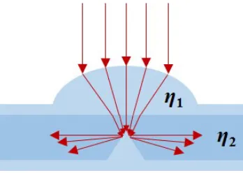
All materials exhibit some degree of absorption, reflection and transmission of light and each
occurs from a single interaction: an electron absorbs a photon [34]. The absorption of photons
occurs in anexactopposite manner to which they were created. There is emphasis on the term
exactbecause for an electron to absorb a photon the energy level of the photon must precisely
match the original high-to-low energy state transition which created it. Any photons that do
not match these required energy levels are simply ignored by the electron and essentially pass through the medium without any interaction with matter. After absorbing a photon the electron
is then in an excited state and is thus unstable. This electron now has two options: transfer
that energy elsewhere or re-emit an equivalent photon. If the absorbed energy is equal to one
of the electron’s natural frequencies of vibration (Eq. 2.3) then resonance will occur which
increases those vibrations further causing interactions with neighbouring atoms and ultimately
converting the absorbed photon into thermal energy. An electron’s natural frequencies are
de-pendent upon the molecule(s) and crystalline structure it composes. If the energy absorbed
does not match an electron’s natural frequency then the electron, being in an unstable excited
state, will fall back to a lower energy state to re-emit an equivalent photon to be later absorbed by subsequent electrons. The re-emitted photons are now considered either reflected or
trans-mitted where the interface between two separate media dictates whether the photon is sent back
within the same medium (reflection) or sent into the new medium (transmission). Figure 2.3
depicts a simple illustration of many photons interacting with a new medium. A portion of the
photons are absorbed, reflected and transmitted upon the medium where the amount of each
are dependent upon an object’s surface roughness and the atomic structure which makes up the
object. There are two main types of reflection: diffuse and specular (which can also apply to refraction). Diffuse reflection is when light gets reflected at many angles. Light will reflect in many angles offa rough surface, but will also transmit into the irregularities of a surface to reflect multiple times within the molecular structure before escaping back in the general
direc-tion to which it entered. Specular reflecdirec-tion is when light gets reflected at the same angle and is
capable of forming images. A very smooth surface, such as a mirror, will create images using
specular reflection as the light is sent back at its incident angle. This is due to a tightly packed
molecular structure with many free electrons that will not allow light to enter. Conductors,
such as many metals, have tightly packed molecules in a lattice structure with free electrons,
thus light is mostly reflected via specular reflection when these conductors have polished
sur-faces. Glossy paints or polished non-conducting surfaces are examples where both diffuse and specular reflection occur.
Figure 2.3: How light interacts with a new medium to become absorbed, reflected and trans-mitted.
The term transmittance is used to describe the fraction of propagating light which
trans-mits through a medium. Alternatively, the term attenuation is used to describe how much
light is lost through a medium and can be defined as either a fraction or in decibels per unit
length. The transmitted intensity of light through a medium will depend upon the amount of
incident light that was reflected upon entering the medium and the amount of light absorbed through the medium. Since the absorption of light occurs from the specific energy levels of
electrons in atoms, it is important to consider the wavelengths of light which will be used in
a device’s application when selecting a material. For example, glass would be a poor choice
of waveguide material for an application involving UV light (10−380 nm) as it absorbs these
wavelengths [35]. This means that glass’s crystalline structure and molecules share natural
incoming light and electrons not having many natural frequencies which coincide with the
visible spectrum of light. Additionally, there must be no gaps or holes in the material’s
molec-ular structure which causes the scattering of light. Water and snow, both consisting of H2O
molecules, are great examples where light scattering effects transparency. TheH2Omolecules
have very few natural frequencies which absorb visible light. However, since snow has many gaps of air or gases within it while water has none, one appears transparent while the other
does not; the lack of transparency is due to the scattering of light.
In a transparent material with no gaps or holes, visible photons are continuously being
absorbed and re-emitted throughout the medium. This absorption and re-emission of photons
from atom to atom in any medium is known as light propagation and is how light travels
through different media. As previously mentioned, the speed of light in a vacuum,c, is equal to 299 792 458 m/s. However, when light travels through a medium filled with atoms, such as visible photons through a solid transparent medium, the light appears to be slowed. There are
two theories that contribute to the change in apparent speed of light in different media. The first theory is the photon absorption-emission theory which describes a small delay between the absorption and re-emission of photons from atom to atom, but the light is still travelling
atc in a vacuum between each interaction [34]. The second theory is the interference theory
which attempts to explain the observable phase velocity direction change of light entering a
new medium while its frequency remains constant. The interference theory can be understood
from Maxwell’s equations for electromagnetic waves in a vacuum [36] (See AppendixA.3).
To understand the macroscopic propagation of light, it is important to realize how a photon
actually travels. When a photon moves from point A to point B it will simultaneously take
every possible path to reach its destination where the actual path it takes can only be explained
using QED. This is known as Fermat’s principle [37] (see AppendixA.4) and for simplicity’s
sake, the basic understanding required is that a photon travelling from point A to point B will always attempt to choose the path that takes the least amount of time: a straight line. Thus, in
this research light is depicted as rays. Figure2.1in Section2.1and Figure2.3above illustrate
examples using straight rays to describe light. It is only necessary to consider light as waves
and particles when photons interact with new media of matter whose geometric dimensions are
close to or smaller than the wavelengths of propagating light; this information is extracted into
2.2.4
The Law of Refraction and Total Internal Reflection
When light enters a new medium at any angle other than 0◦ from the normal it is not only transmitted with a change of speed, but it also undergoes a change of direction. The change in
direction is due to the change in phase velocity,v, which is the speed the crests of a wave moves
at while its frequency remains constant. This phenomena of light changing velocity upon
en-tering new media is known asrefractionand is one of the key properties for manipulating light
at the macroscopic scale. All lenses in commercial optical devices function using refraction.
Refraction is described by Snell’s law which can be derived with Fermat’s principle of least
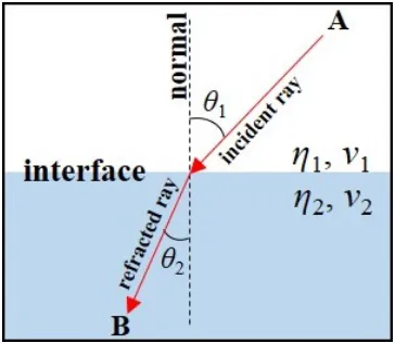
time [37]. Snell’s law states that for two differing media and a wave with a single frequency, the ratio of the sines of the angle of incidenceθ1and angle of refractionθ2is equivalent to the
ratio of phase velocities between the two media [38]. Snell’s law is given by:
sin(θ1)
sin(θ2)
= v1 v2
(2.4)
Snell’s law can also be described in terms of the materials’ index of refraction,η, which is a
dimensionless number that describes how light propagates through a medium at an apparent
slower velocity and is given by:
η= c
v (2.5)
wherec is the speed of light in a vacuum and vis the phase velocity of light in the medium.
After substituting Eq.2.5into Eq.2.4, Snell’s law becomes:
sin(θ1)
sin(θ2)
= η2 η1
(2.6)
Figure2.4illustrates this phenomena of refraction by using a ray of light travelling from point A to point B in the least amount of time. Since the phase velocity of light is lower in the second
medium (v2 <v1) the angle of refractionθ2is less than the angle of incidenceθ1.
Light’s incident angle upon a new medium will dictate how much of the light is reflected
or refracted by the new medium. Fresnel equations (see AppendixASectionA.1) can be used
to describe the complex behaviour of light between media of differingη[39]. There are a few special cases with Fresnel equations which depend on a light ray’s angle of incidence. Light
polarization, the single plane oscillation of light waves, is a familiar special case for refracted
light that occurs at a specific angle between media known as Brewster’s angle (see AppendixA
SectionA.2) [40] and is how polarizing sunglasses work. Another special case which is most
important to this research occurs when light propagates from a high η medium to a low η
Figure 2.4: Refraction of light from point A to point B at the interface between two separate media using Snell’s law (Eq.2.4&2.6).
is known as a critical angle, θcrit, where any incident light at or greater than this angle will
be completely reflected back into the higher ηmedium. This phenomenon is known as total
internal reflection (TIR) and is another key property for controlling and manipulating the flow of light [41]. TIR is how all waveguides work to transmit light from one end to the other and
occurs when Snell’s law (Eq.2.6) becomes impossible to satisfy where sin(θ2) must be greater
than one. Figure2.5illustrates TIR once this critical angle is reached. The critical angle,θcrit,
can be found by rearranging Snell’s law whenθ2 =90◦or sin(θ2)= 1. θcritis then given by: θcrit =arcsin η2
η1
!
(2.7)
Figure 2.5: Refraction of light at the interface between two separate media using Snell’s law (Eq.2.6). Ifη1>η2andθ1 ≥θc than the light is totally internally reflected.
stays trapped within a medium of higherη compared to surrounding media. For illuminators
and collectors small geometrical structures, termedMOSswith lowerηcan be embedded within
the medium to accurately control how much light escapes or stays trapped at certain regions.
For example, in illuminators MOSs such as wedges can be used to modify the angle of a portion of the total propagating light rays so thatθ1becomes less thanθcritand this light will now escape
the higherηmedium upon interaction with the next interface. The function of these MOSs and
their geometrical shapes are detailed in Section2.4.3.
2.2.5
Limitations of Light as Optical Device Design Constraints
A working knowledge of light and how it propagates through a material allows for some design
constraints and insight for illuminators and collectors. The following three constraints and
material selection insight have been arbitrarily defined from the working knowledge described
above.
Constraint: Micro-optical Structure Size
The first constraint considers the interference theory of light mentioned in Section2.2.3. Thomas
Young performed an experiment in 1801 using two small slits with dimensions close to the
wavelength of visible light [42]. When light passed through these slits Young observed an
in-terference pattern on the screen. This inin-terference pattern was caused by a phenomenon called diffraction where light sightly bends as it passes around the edge of an object [43]. The amount of bending depends on the relative size of the wavelength of light to the size of the opening.
Therefore, in relation to the design of illuminators and collectors it is important to set a size
limit on the diffusing and concentrating MOSs. MOSs that are too small within the nanometre scale will cause interference and scattering of the propagating light waves which is difficult to control due to the randomness of light scattering at that scale. This will impede upon the
intended affect to uniformly illuminate or collect light if the application requires it. There-fore this first arbitrary constraint sets a minimum feature dimension size of 0.005 mm or 5µm
which is five times larger than low-level IR light.
Constraint: Layer Thickness
The second constraint relates to the thickness of the medium in which light will propagate
through the flexible illuminators/collector. Once a medium with propagating light due to TIR becomes thinner than the wavelength of light, it may interfere with itself and simply ignore
a boundary change and escape. For example, when the thickness of a medium is a
lengths it may interfere with what is called an evanescent wave. A side effect of TIR described in Section 2.2.4is where an evanescent wave appears beyond the interface of media.
Essen-tially, even though the entire incident light wave is reflected back into the higher η medium,
there is some penetration into the lowerηmedium at the boundary. Thus, when the higher η
medium becomes thin towards the wavelengths of propagating light it can interfere with this
evanescent wave and the transmittance will decrease. Therefore, the multiple layers of
illumi-nators and collectors should not be too thin to affect the larger wavelengths in the optics region (Figure 2.2). Thus, an arbitrary constraint can be made to design the layers of these optical devices at a minimum thickness no thinner than a sheet of paper (0.05 mm). The termthinin
this research will revolve around this scale where layers can be as thin as 0.05 mm or as thick
as 5 mm depending on the intended application.
Constraint: Refractive Index Consistency
The third constraint is simply to keep the refractive index, η, constant throughout each layer
within the optical device. If η varies through a medium the light can be bent or focused.
Additionally, since transmittance and refraction are relative to the wavelength of light a change in ηmay begin to absorb certain wavelengths. This type of material is known as a
gradient-index medium which can be very difficult to control and fabricate. Gradient-index mediums are seen in the human eye where the η of the lens varies from approximately 1.406 in the
central layers down to 1.386 in less dense layers of the lens [45]. Therefore, if attempting to
modify theηof a layer, this change inηshould stay constant throughout the layer to avoid any
unintended changes in the propagating light’s direction and transmission. Alternatively, if the
ηcan be precisely controlled new potential design options may open for controlling the flow of light; however, this is beyond the scope of this research.
Insight: Flexible Transparent Material Selection
Insight towards creating or modifying flexible materials that transmit light within the optics
spectrum is valuable information. This may be potentially useful in future work (Section5.3)
considerations for synthesizing new flexible polymers or modifying the refractive index,η, of
absorp-tion, reflection and transmission of photons in different media which were dependent upon the electron configuration and crystalline structure within the media. When optical transparency
is a desirable aspect for a material, there are several properties at the molecular scale involved,
however two key properties define most solid transparent materials. The first key property was mentioned in Section2.2.3which described a consistent crystalline structure with no gaps or
holes was essential to prevent the scattering of propagating light. The second key property is
a solid material’s band gapwhich is the energy range where no electron natural frequencies
can exist [34]. The band gap is typically described in electron volts (eV), a unit of energy
equal to 1.6 ×10⁻¹⁹ J. Using Eq. 2.1 and converting to eV, visible light is within the range
of approximately 1.8 eV to 3.1 eV meaning if a material’s band gap is greater than 3.1 eV it
will be transparent due to no natural frequencies available to resonate. Thus, when an electron
is excited past the band gap it simply falls back down and re-emits an equivalent photon as
described in Section2.2.2. Insulators often1 have band gaps which are greater than the range of visible light and do not have a “sea of electrons” (found in conductors) to reflect and block
light from entering in the first place. For modifying the refractive index of existing
transpar-ent materials the dielectric constant is closely related. To show this, the phase velocity in a
medium is inversely proportional to the permittivity,µ, and the permeability, of the material
and is given by [34]:
v= √1
µ (2.8)
Substituting Eq.2.8into Eq.2.5gives:
η= c
v =
√
µ
√
0µ0
= √rµr (2.9)
whererandµrare the relative permittivity and the relative magnetic permeability, respectively.
Finally, since most materials are only slightly magnetic (µr 1) Eq.2.9simply becomes:
η √r (2.10)
Relative permittivity, r, is also known as the dielectric constant. Therefore, a transparent
material’sris directly proportional to its refractive index,η. This is particularly useful when
searching for initial candidates or for tuning a material’s ηby adding high r particles to the
material’s matrix. Section2.6.3describes adding highrnano-particles to the chosen material
This information can be used as a guideline for the design and transparent material selection
for illuminators and collectors as well as any other potential optical device.
Table 2.1: Initial design constraints/insight for flexible diffuser and concentrator applications. Parameter Constraint/Insight
Feature size > 5µm to avoid light scattering and interference
Propagating layer thickness > 0.05 mm to avoid interference effects
Propagating layer material Must have constantηto avoid unintentional bending, fo-cusing, and absorption of light
Transparency Related to band gap and insulators
Refractive index (η) Related to the dielectric constant (r) for modifyingη
2.3
Operating Principles of Flexible Optical Devices
Optical devices such as fibre optics or simple waveguides used in communications utilize the
phenomenon of TIR described in Section2.2.4to function. Fibre optics exist as two transparent
materials with different indices of refraction, η. Figure 2.6 illustrates the flow of light in a simple fibre optic cable’s cross-section using rays. The light propagates through the core (η1)
and is totally internally reflected by the cladding (η2). Therefore the η of the core must be
higher than the ηof the cladding (η1 > η2) for TIR to occur. The core and cladding in fibre
optic cables are cylindrical and are designed to transmit light in the form of data from one end
to the other. The core and cladding typically consists of different transparent hard plastics or glass materials. These cables are flexible to a certain degree since the diameters of both the
core and cladding are very small. The ability to be considered flexible with rigid materials due
to small diameters can be understood from the classic bending stress in a beam equation [46]:
σ= −Mxy
Ix
whereσis the bending stress,Mxis the moment about the neutral axis,yis the perpendicular
distance to the neutral axis, and Ix is the second moment of inertia about the neutral x-axis.
Looking at the second moment of inertia for a cylinder’s cross-section shows that it is
propor-tional to the quartic of the diameter:
Ix,circle= πD4
64 (2.12)
Therefore, sinceDis in the numerator in Eq.2.12andIx is in the denominator in Eq.2.11the
stress due to bending in a cylinder decreases rapidly as the diameter shrinks. This applies for
all geometrical shapes and is why thin objects such as sheet metal are easily bent. However,
like all hard materials with a high elastic modulus,E, there is a limit to bending before plastic
deformation or breaking occurs. Practical usage of fibre optic cables typically does not require a high degree of bending during usage. If sharp bending is a requirement, there exists
right-angled mirrored Sections to direct light around tight corners.
Figure 2.6: Illustration of light rays propagating through a fibre optic cable’s cross-section. Light propagates through the Core and reflects off the Cladding from TIR. There is often a Jacket for protection.
2.3.1
Structure of an Optical Sheet Device
Optical sheets function in a similar manner to fibre optic cables. In fact, the cross-sectional
illustration in Figure 2.6 above properly depicts the cross-section of a simple waveguiding sheet having a jacket and how it functions with the same behaviour. Instead of a core and a
single cladding enveloping it, a sheet must consist of a set of layers in a cladding-core-cladding
fashion for TIR to occur. An optical sheet, or in this example a strip, is often more desirable
than cylindrical cables in optical interconnects [21–25] due to the ability to have multiple
occurs some angles of propagating light will change and become lower than the critical angle,
θcrit, between the core’sηand the cladding’sη(Eq.2.7). When the incident angle between the core and cladding mediums becomes lower thanθcritthe propagating light will no longer totally internally reflect back into the core medium. The light that is not internally reflected will then
escape into the cladding and eventually into the next medium (air). Light propagates at many
angles, thus not all light will escape simultaneously upon initial bending. Instead, an
increas-ing amount of light will escape as the bendincreas-ing radius decreases causincreas-ing more of the light’s
incident angles to become lower thanθcrit in the bending region. As Eq.2.7depicts, a greater
∆ηbetween the core and cladding mediums will allow for a larger θcrit; thus, less propagating light will escape during bending. Reducing bending losses in optical communication is a large
area of study where achieving smaller bending radii with minimal attenuation loss is desirable,
especially in optical interconnects [21–25].
2.4
Characteristics of Optical Light Concentrators
(Collec-tors) and Di
ff
users (Illuminators)
Illuminators and collectors are not designed for light transmission from point A to point B.
Instead, these sheets may comprise of multiple layers consisting of many MOSs which
redi-rect light within the medium. Such large area waveguiding designs may act as diffusing sheets (illuminators) or light concentrating sheets (collectors). Rigid collectors [1–4] are typically
de-signed for solar energy collection to concentrate light towards a smaller region where efficient solar cells convert the light to electricity in a cost-effective manner. Rigid illuminators [5–10] are often designed as diffusing panels for electronic displays known as light guide plates. Both collectors and illuminators utilize TIR with MOSs to control the incoming or outgoing light.
These devices have many potential applications as they can manipulate light in a uniform or
non-uniform fashion depending on the location and geometry of MOSs embedded in the
de-vice. This section will briefly describe the key parameters these devices function upon as well
2.4.1
Source Lighting
Collectors and illuminators function in a similar, yet opposite manner. Figure2.1in Section2.1
depicts a simple illustration of this similarity. The source lighting for a collector is always
outside the device and lands upon its largest functional surface where it collects, redirects and essentially concentrates the light to an edge(s) or point(s) within the core medium. Source
lighting for many existing collectors [1–4] is typically the sun as these are designed for solar
energy collection. An illuminator takes an intense light source, such as an illuminated edge,
and redirects, reflects and essentially diffuses the light out of the largest functional surface. These light sources are often fixed to the edge of the device [5–10] for propagation through the
core medium. It is important to note that in both illuminators and collectors the incident and
diffused light never propagate entirely in the exact same direction. Since light flows as a wave and reflects offmany objects in the environment there are many incident angles of light upon collectors. Similarly, in illuminators the initial edge-lit source will propagate light at many different angles which will undergo TIR multiple times until escaping from diffusing MOSs. The diffused light in illuminators will also propagate out of the functional surface at many different angles. Therefore, it is important to have a robust design capable of functioning with as many different angles of incoming and outgoing light as possible. Alternatively, if a single polarization of light is desired, Brewster’s angle described in Section 2.2.4 could be used to
achieve such an affect and is ultimately up to the designer to achieve it.
2.4.2
Selection of Core and Cladding Material
For a simple waveguide to function properly using TIR, the core and cladding must have
dif-fering material properties in order to have a∆ηbetween the two. Section 2.2.5described how the dielectric constant is closely related to the η of transparent materials. Since the ηof the
core material must be higher than the η of the cladding material for TIR to occur, Eq. 2.10
shows that the core material must also have a higher dielectric constant than the cladding. This
can be used for the initial material selections, however there are more properties to consider
than only theη. A key property to consider is the compatibility in bonding between the two
materials. If the two materials cannot naturally adhere to each other then creating a layered cladding-core-cladding structure will become increasingly difficult. Using compounds such as an intermediate adhesive layer between the two materials for bonding is not a worthy solution
as the thin adhesive layer will have its ownηand will essentially end up acting as the cladding
layer instead of the intended material. Therefore, the two materials must bond without any
in-termediate help from other materials. If the two chosen materials do not naturally adhere, there
damage and is determined by the material’s stiffness which encompasses the yield strengths and geometries of the device’s materials. Equations2.11 and2.12in Section2.3 showed that
as the diameter of a beam decreases, the stress due to bending rapidly decreases, allowing for more deformation before permanent damage. This is similar for the thickness of an object, such
as a sheet, and relates to the geometric portion of stiffness and flexibility. The other portion depends greatly on the elastic modulus of the material. Both can be understood from the classic
axial stiffness equation:
k= AE
L (2.13)
where k is stiffness, A is the cross-sectional area, E is the elastic modulus, and L is length. Since both Aand E are both in the numerator, the stiffness of an object will decrease as the thickness and modulus decreases. These properties ultimately specify the strain exerted within
the deformed device. Elastic materials, such as rubber, perform exceedingly well in this regard
since they have a low elastic modulus and return to their original shape and size when the
forces which deformed them are removed. In general, materials withE <5 MPa are often very
elastic (i.e. natural rubber has anEof 1−5 MPa [48]).
Assuming the materials are capable of naturally bonding, if their stiffness differ by a large margin then during deformation there can be concentrations of stresses at important regions
within the optical device, such as the plane where MOSs for diffusing or concentrating light exist. This can potentially permanently damage these MOSs and compromise the functionality
of the device. Hu et al.[23] explains this challenge in waveguide and photonic design when using different thin stiff materials. They describe a “neutral plane” where the strain during deformation vanishes and how to determine or specify its location by stacking multiple thin
materials. By forcing the neutral plane to exist within the optically featured core layer, Huet
al.[23] were able to achieve a minimum bending radii of< 0.5 mm despite the poor mechanical
strength of the glass materials used.
In conclusion, several properties must be considered when selecting the core and cladding
materials of flexible optical devices. Other considerations could even involve slow chemical
reactions between the two materials that alter the η over time. Therefore, the two materials
must be considered together for compatibility issues and not separately solely for theirηand
same base material in both the core and cladding layers. Using the same base material better
ensures compatibility between layers for bonding and bending stresses. This is known as a
monolithic design and is discussed in Section2.5.3below.
2.4.3
Importance of Micro-optical Structures
To manipulate and control the flow of light through an optical device, micro-optical structures
(MOSs) must be present to reflect and refract the propagating light rays as desired. MOSs
require very smooth surfaces to prevent the apparent randomness created due to the diffuse reflection and refraction of light that was discussed in Section 2.2.2. TIR or a metallic
mir-rored finish allows for reflection to occur offMOSs while refraction will occur if theθcritis not reached (Eq.2.7) or the light is traversing from a lower ηmedium to a higher ηmedium such as a focusing lens. Both cases require the MOSs to have a differentη or reflective properties than the medium which the light is propagating within. The geometry, size, η, and locations
of MOSs determine their function. Figure 2.7 illustrates three common MOS geometries:
Pyramid/Cone, Convex Lens, and Wedge. These MOS geometries are commonly used in illu-minators and collectors. For example, in illuillu-minators with an edge light source wedges can be
used to redirect propagating light rays to change their next incident angle upon the cladding to
be less than the critical angle, θcrit; thus, light rays escape the device. Illuminators can utilize
many different types of geometries to function since the propagating light often only needs a small change in angle to escape the core medium. MOSs such as holes, cones, dots, and even
scores can redirect the light to a new angle which allows it to escape the device. For example, Huanget al.[5] and Parket al.[6] use micro-sized dots to diffuse light out of their designs.
Figure 2.7: Cross-sectional illustrations of common micro-optical structures (MOSs). a) Pyra-mid or Cone for redirecting incident light into the core layer in many planar directions. b) Convex Lens for focusing incident light to a focal point below. c) Wedge for redirecting inci-dent light in a general direction; i.e. to escape the core layer.
angles within the core medium (η2) and if the angle is also greater than θcrit between η2 and η1 it will reflect through the core medium due to TIR. Due to the geometry of a pyramid the
incident light is now redirected to all four edges of the collector where sensors or photovoltaic
cells may exist to harvest the light. Bouchard and Thibault [2] and Karpet al.[4] use similar
light collecting techniques with their rigid collector designs.
Figure 2.8: Cross-sectional illustrations of a MOS combination using a convex lens and a pyramid. The lens focuses incident light onto the pyramid which redirects the light throughout the core layer.
The size of MOSs is also very important and, in general, smaller MOSs are often more
desirable due to the ability to fit more within an area to create a more uniform distribution of
incoming and outgoing light. The size of the pyramid relative to the lens and core thickness
illustrated in Figure2.8is actually much too large for light collection to be efficient in a light collector with many of these MOS combinations. Light that is redirected offthe pyramid will be propagating through the core medium and since the height of the pyramids are close to
the thickness of the core layer (η2) the rays have a high chance of striking adjacent pyramids.
Therefore, in this example small and short pyramids relative to the lenses and core thickness, respectively are more efficient as there is less of a chance for redirected light to strike another pyramid on its route to the edges. Xieet al.[49] use prisms that are 1.8% the size of the lenses
where the prisms have a base width of 90µm and the lenses have a diameter of 5 mm to achieve
an overall theoretical optical efficiency of 70%. This reduction in pyramid size relative to the lenses shows why the location of MOSs is also quite important. If the centre of the pyramid
to all four edges of the collector. Additionally, due to the micrometre scale MOSs are within,
a slight alignment issue of a few micrometres can cause the focused light to miss the pyramids
entirely. Therefore, accuracy of dimension, surface finish, materialη, and alignment of MOSs
is crucial in fabrication to ensure an efficient and functional product.
2.4.4
Importance of Core and Cladding Layer Thickness
A consistent and accurate thickness of the core and cladding layers is essential for a functional
design. If a layer has a varying thickness then the angles of propagating light will slowly change
and may unintentionally escape in certain regions of the core medium. If the thickness of a
layer is not accurate it can cause unintentional interactions of light with MOSs and compromise
the functionality or efficiency. Section2.4.3above described a MOS combination with a lens’ focal point hitting a small pyramid to redirect light. The thickness of layers also controls where
the focal point of this lens will be upon the pyramid. Again, due to the micrometre scale of
MOSs if the layer is thicker by even a few micrometres the focal point of the lens can miss the
pyramid entirely. It is also important to mention that from Section2.2.5once the layers become
very thin, approaching low multiples of the wavelength of light, issues with interference begin
to occur. Therefore, a consistent and micrometre-accurate thickness of each layer must be
achieved during fabrication for a functional and efficient product. Section 2.7.3below details fabrication techniques used in literature to accurately control layer thickness.
2.4.5
Characteristics of Uniform and Non-uniform Illumination
Uniformity is an important property for many applications of illuminators and collectors and is
controlled through design. For collectors the concentrated light is being directed to a specific
location within the optical device, such as a point or edge where the uniformity of incident
light at this location is far less important than the initial capturing uniformity. This is relatively
simple to control with consistent repeating concentrating MOSs. A collector may require
non-uniform initial light concentration in some applications and it is up to the designer to distribute the concentrating MOSs as required. For illuminators it is more complex and is highly
depen-dent on the application and intended illumination effect. Consider a back-lighting application used in electronic displays where the source light is an intensely illuminated edge that is
dif-fused out of the large surface facing the user.
In this application uniform illumination is of high concern to produce a bright even picture
for the user. Figure 2.9 illustrates a simple non-uniform illuminator using diffusing wedge MOSs where the thickness of arrows represents the amount of light escaping in the general
Figure 2.9: Non-uniform light diffusion in an illuminator. The thickness of arrows represents the amount of light escaping in the general region.
core layer a relatively large portion of the light is reflected and escapes upon hitting the first
diffusing MOS. Less light hits subsequent MOSs until almost no light is available at the far end of the illuminator.
Figure 2.10illustrates two common techniques to control uniformity: size and density of
diffusing MOSs. Figure2.10 on the left shows how the size of MOSs can control uniformity. MOSs closest to the source will have the most potential light to interact with. However, less
light will interact with smaller MOSs allowing for a larger portion of the initial light to continue
propagating towards subsequent MOSs. Figure2.10 on the right shows how the spacing, also
known as density, of same-size MOSs can control uniformity. Again, MOSs closest to the
source have more light to interact with, but in this instance as the spacing between MOSs
reduces the light interacts with more MOSs per unit length so as the intensity of light reduces
the amount being reflected out also increases creating a uniform illumination. This density technique is generally easier to fabricate compared to the size technique due to the repeating
geometries of MOSs. With controllable illumination, an example of an intentional non-uniform
illuminator would be a sign where only the letters or image outlines are illuminated. The exact
placement, density and size of diffusing MOSs will dictate where the main illumination occurs in this example. It is also important to note that smaller MOSs in illuminators will give a better
resolution of light which will appear more uniform.
![Figure 2.2: Optics region of the electromagnetic spectrum. (Modified from [32])](https://thumb-us.123doks.com/thumbv2/123dok_us/1997676.1264476/22.612.202.431.169.532/figure-optics-region-electromagnetic-spectrum-modied.webp)