1803 IJSTR©2020
www.ijstr.org
Efficient Framework For Column Reduction
Multiplier In Vlsi Applications
R Arun Sekar, S V Ramanan, Sanjeevi Pandiyan, Rajan Cristin
Abstract: Nowadays in VLSI innovation size, power, speed and cost are the principle plan contemplations in any circuits. As the quantity of included activities in ordinary multipliers are more which brings about increment in delay. Consequently, the circuits structured with ordinary multipliers will expend more power and have less speed. In this paper, design and implementation of FPGA based 32-bit Wallace multiplier, Dadda and modified multiplier has been analysed. These multipliers were designed using Verilog HDL, simulated and synthesis is done in both RTL compiler utilizing Xilinx Vivado and executed on Zynq 7000 arrangement FPGA board.
Index Terms: Column reduction multiplier, Dadda multiplier, Modified Wallace tree multiplier, Peres gate, Reversible logic, SMG gate, Wallace tree multiplier.
—————————— ——————————
1.
INTRODUCTION
Multiplication [1] can be performed in quicker way by utilizing column reduction multiplier (CRM). A portion of the models for segment decrease multipliers are Wallace tree (WT) multiplier, Dadda and Modified Wallace tree (MWT) multiplier. In spite of the fact that WT, Dadda and MWT are utilized for quicker augmentation, their speed can be additionally expanded by expanding the speed of the adders engaged with it. CRM are favored over the cluster multipliers since their postponement is relative to (log2n) for the multiplier width. For the exhibit multiplier it is relative to n times the multiplier width. There are three significant strides in CRM. For a nxn multiplier,
1. n2 incomplete items are produced. These incomplete items are produced by duplicating the multiplicand bit with the multiplier bit and playing out the consistent AND activity for each piece esteem.
2. The fractional items are diminished through a few phases until two lines in definite stage are accomplished. The decrease procedure is performed by counters or blowers or adders.
3. At long last the two lines in the last stage are included by utilizing convey spread snake and the outcome is determined as result of multiplicand and multiplier.
2
RELATED
WORKS
Koti lakshmi et al. [2] talks about the Vedic Multiplier usage utilizing reversible entryways. Reversible rationale is promising which shows zero power scattering hypothetically.
So applying reversible rationale in Vedic Multiplier circuits demonstrated to be an effective situation. The quantity of consistent sources of info, trash yields and rationale doors is definitely diminished by utilizing reversible rationale. Speed and power use is additionally diminished with increment in
zone. Sushma R.Huddar et al. [3] structured rapid multiplier utilizing 4:2 and 7:2 compressors. Halfway item count is performed by the blowers and ordinary adders are utilized for the expansion of the last item figuring. The speed of this multiplier is multiple times quicker when contrasted with the cluster multiplier with increment in intricacy. Mandala Sowjanya et al. [4] examined the sketching out technique of various essential rationale plan entertainment in advanced snake as speed of expansion is confined by engendering of bring through viper. This work shows the choice of picking the proper adder topologies. Quickest multiplier is structured dependent on the change in the adder topologies. Vijay K Panchal et al. [5] talked about the usage of multiplier utilizing reversible rationale entryways. The principle bit of leeway of utilizing the reversible doors is its zero power dispersal under perfect conditions. Structure alterations are performed in the reversible doors to decrease the trash bits and steady sources of info. In this work, multiplier is structured dependent on Toffoli entryway, Peres door and Double Peres door. The proposed reversible multiplier has a superior exhibition with respect to trash bits, consistent sources of info and equipment multifaceted nature. H. R. Bhagyalakshmi et al. [6] brief about the quantum cost (QC), where QC of the reversible logic is reduced by reducing the number of reversible gates. QC is the cost of the primitive reversible basic logic gate involved in the circuit to realize it. Each reversible gate has a certain fixed QC. So in to obtain minimum QC specific designs of reversible gates should be selected and implemented in the multiplier for its efficiency. As a result, the delay is reduced with a slight increase in area. M. Shams et al. [7] proposed an efficient multiplier by using a newly proposed MKG reversible full adder. The MKG gate has depth of four. It produces two garbage outputs, required sum and carry output. It is a single reversible gate capable of performing the entire full adder circuit operation. Advantage is the less logical calculation and less quantum cost with increase in delay. H. Thapliyal et al. [8] designed multiplier based on the reversible TSG gate. Fredkin (FD) gate is used for partial product generation and later the addition is manipulated by TSG reversible gate. All the existing reversible full adder circuit requires either three or five reversible gates for its full adder implementation. The existing methods produce three to five garbage outputs. The proposed method in this circuit has only one reversible gate for the implementation of the full adder and its unit delay is also one. Less logical calculation with increase in delay.
————————————————
Dr.R.Arun Sekar is currently working as a .Assistant Professor in GMR Institute of Technology, Rajam, Andhra Pradesh, India, PH-9994650100. E-mail: [email protected]
Mr.Ramanan.S.V is presently working as Assistant Professor in PPG Institute of Technology,Coimbatore,Tamil Nadu,India. PH-9843817927. E-mail: [email protected]
Dr.Sanjeevi Pandiyan,Postdoc Scholar,Key laboratory of Advanced Process Control for light Industry,Ministry of Education,Jiangnan University,Wuvi 214122,China.
PH-9003540336. E-mail:[email protected]
1804
3
EXISTING
METHODOLOGIES
3.1 Wallace multiplier
WT multiplier was first designed by Wallace [10,11] in 1962. This multiplier is based on the concept of grouping the partial products into groups of three. Each grouping of three are then reduced by using full adders and half adders. Three important steps to be followed during the reduction of partial products are as follows. First the section containing the three bits are reduced by using the full adder circuits. Then the section containing the two bits are reduced by using the half adder circuits. If any single bit is left behind in each stage of separation, then they are passed to the next stage without processing. This decrease strategy is implied to each progressive section till just 2 columns are left. The last two lines are added with a carry propagate. Notable rapid multipliers are WT multiplier which utilizes carry save adders (CSA) to lessen N-columns of incomplete items to two-line grid. The carry save adders are customary full adders (FA) whose carry are not associated with the goal that three words are taken in and two words are yield. The Wallace multiplier utilizes half adders (HA) and FA in their reduction stage. An adjusted outline is displayed that significantly diminishes the half adders. In WT multiplier, in the second step of reduction the Wallace approach utilizes a few phases of
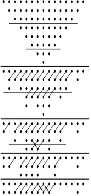
FA and HA as CSA‘s. The grouping of 8x8 WT multiplier is shown in figure 1.
3.2 Dadda multiplier
When compared to the WT multiplier design, Dadda multiplier [12] has lesser delay. Reduction is taking place at each stage. To determine how number of reduction stages are required at every stage is determined by the formula. Here the reduction starts from the last stage. The last section has a stature of 2 lines. The former section tallness can be no bigger than (3*successor stature/2). This gives 2, 3, 4, 6, and so on as the greatest statures for the different past stages. The Dadda decrease at that point utilizes simply enough FA and HA to accomplish the breaking points for the section decrease stature. The schematic of 8 by 8 Dadda multipier is shown in the below figure 2. Here the reduction takes place in four stages which is similar to WT reduction stages. But the only difference is the number of FA and HA being utilized. The third intermediate section requires carry propagate adder.
1805
Fig. 2. Grouping of Dadda multiplier
2.3 Modified Wallace tree multiplier
The MWT multiplier was designed mainly to decrease the number of HA used in the circuit. Mainly in the partial product reduction FA and HA are generally used and finally they are passed to the carry propagate adder. The main aim of using the FA and HA is to reduce the number of partial products and reduce them into two single sources and finally pass them to the carry propagate adder. FA takes three bit of inputs and reduce them into two single sources, similarly HA works on two-bit sources and reduce them to two single source output bits. So, it is clear that HA are not generally used in the reduction of bits. The quantity of the partial items is not decreased by the presence of HA, but they are only used for the relocation of the bits. One might say that HA don't perform any contribution in decreasing the multifaceted nature of the
multiplier. The MWT wants to limit the utilization of half adders so as to improve the effectiveness for CRM. The reduction method utilizing the MWT multiplier is appeared in Figure 3.
Fig. 3. Schematic of MWT multiplier
3
PROPOSED
METHODOLOGY
3.1 Reversible logic
Any number juggling activity can be performed utilizing the
1806 strategy for reversible procedure which permits least number-
crunching execution. A basic situation for accomplishing this condition is that the number juggling plan associations ought to be of coordinated. Reversible rationale has created as another blueprint strategy to the standard rationale, provoking low power utilization and least area. For achieving low power, reversible justification technique for task is executed. Reversible rationale [9] has amazing thought in the late years on account of their ability to lessen the power dispersal which is the essential in low power VLSI diagram. It has wide applications in low power CMOS and optical information planning, quantum estimation and nanotechnologyReversible rationale segments are relied upon to recover the state of contributions from the yields. Reversible door is info and n-yield rationale. It is said to be coordinated mapping wonder. The yields can be effectively decided from the data sources then the information sources can likewise be acquired from the yields. Direct fan out isn't permitted during the union of reversible circuits since one to numerous idea isn't reversible. Be that as it may, fan out in the reversible circuits can be accomplished by using extra entryways. The multifaceted nature and the presentation of the circuit are dictated by number of elements as pursues: All out number of reversible entryways utilized in the circuit
Any sensible capacity can be combined by using a steady info that are kept up at 0 or 1 The quantity of unused yields called trash yields which can't be maintained a strategic distance from as they are utilized for reversibility. So as to understand the circuit, the quantity of crude reversible doors ought to be noted. This figuring is called as Quantum cost (QC). Further it is characterized as the expense of the circuit which is controlled by the expense of the crude entryway.
3.2 Peres Gate
One of the 3*3 gate which uses the reversible operation is the Peres gate. It has three input sources and three output operation. One to one mapping is seen in this gate as it is reversible. The output is given by the following expressions X=A, Y=A^B, Z=AB^C. The Quantum cost of this Peres gate is 5. The pictorial representation of this gate is shown in the below figure 4.
Fig. 5. Schematic of Peres full adder
3.3 Peres full adder gate
The combination of two Peres gate can be utilized to realize
the Full adder (FA). Figure 5 shows the schematic of the FA utilizing two Peres gate. This reversible Peres FA gate is used
for the realization of the multiplier. QC of using two Peres gate for the realization of FA is 8.
3.4 SMG gate
One of the 4*4 gate which uses the reversible operation is the SMG gate. It has four input sources and four output operation. One to one mapping is seen in this gate as it is reversible. The output is given by the following expressions to P=A,Q=A^B^D,R=A^B,S=((A^B)D^(A.B^C)) where the inputs are given by four variables A, B, C, D and the outputs are represented by P, Q, R, S respectively. The block diagram of SMG gate is shown in the figure 6.
Fig. 6. Schematic of SMG gate
The truth table showing the sum and carry out operation is mentioned in the following table 1. When the full adder gates are designed using the Peres reversible gate and SMG reversible gate, then the number of reversible gates used for designing FA is 2 and 1 respectively. Further the QC and the transistor cost are reduced from 8 to 6 and 64 to 48 respectively.
Table 1: Truth table implementing the FA operation using SMG logic
TABLE1
TRUTHTABLEFORSMGGATE
Cin B A 0 Q(Sum) S=Cout
0 0 0 0 0 0
0 0 1 0 1 0
0 1 0 0 1 0
0 1 1 0 0 1
1 0 0 0 1 0
1 0 1 0 0 1
1807
1 1 1 0 1 1
4
DRAWBACKS
OF
CARRY
LOOK
AHEAD
ADDERS
Carry chain is the serious issue for any paired expansion. The length of Carry chain is subject to the width of operand bits. As the width of operand expands, the Carry chain length likewise increments. At the point when the Carry proliferates from the Least Significant Bit (LSB) to the Most Significant Bit (MSB), the most dire outcome imaginable happens. Remembering the ultimate objective to improve the presentation of Carry spread adders, it is possible to revive the Carry chain, yet not to get rid of it. Along these lines, most exceptional fashioners consistently fall back on building quicker adders while improving PC plan, since they will in general set the basic way for most calculations. CLA are utilized to diminish
the postponement in RCA (or) to spread the Carry early. In a general sense this adder deals with two activities called generate and propagate. As the bit length of the adder builds, the Carry intricacy additionally increments. In this way, there is a multifaceted nature in structuring higher piece CLA. Along these lines, for the higher piece of CLA's, if the width of the adder expands, the multifaceted nature of the Carry likewise increments. To lessen the delay and to figure the Carry ahead of time, another idea called reversible full adder using SMG entryway is proposed.
5
RESULTS
AND
DISCUSSION
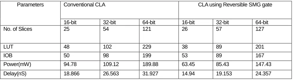
Table 2 : Comparison of area, power and delay of conventional CLA with CLA using Reversible SMG gate
TABLE2
COMPARISON OF CLA WITH CLA USING REVERSIBLE SMG GATE
The input and output blocks (IOB) represent the area. For 16-,32- and 64- bit the area is reduced by 6%,9% and 16% respectively when the conventional CLA is compared with CLA using reversible SMG gate. Similarly, the power and delay are also reduced by 33%,21.71%,22.35% and 20.78%,27.89%,23.71% respectively. In the WT multiplier the partial product reduction stage utilizes carry save adder. These carry save adders are replaced by reversible SMG gate. In the final stage, carry propagate adder is replaced by the newly proposed reversible SMG to produce the final product as the result. Conventional reduction of the partial products at the
intermediate stages and the final stage is performed by the reversible SMG. Similarly, in the Dadda multiplier, the final stage of reduction and the intermediate stage which has full adder combination are replaced with reversible SMG gate. Significance reduction in the area, power and delay is achieved. The MWT reduction technique isolates the lattice into three-row gatherings and uses full adders for each gathering of three bits in a section like the regular WT reduction. A gathering of two bits in a section isn't handled, Single bits are passed on to the following stage as in the ordinary WT reduction. For a few cases, HA are just utilized in the last phase. In the final reduction stage, the carry propagation stage is replaced by newly proposed reversible SMG. In the final carry propagation path of modified Wallace tree multiplier, the reversible SMG is applied. By introducing reversible SMG gate, the gate count can be reduced thereby reducing the power consumption and increasing the speed. So, by applying reversible SMG, the performance can be improved.
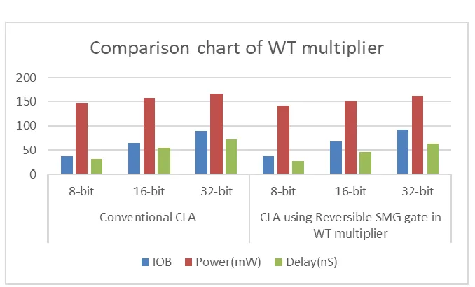
Table 3 shows the comparison of area, power and delay of WT, Dadda and MWT multiplier by utilizing reversible SMG gate as the full adder. Figure 7 shows the pictorial representation of area, power and delay comparison of existing WT multiplier with WT multiplier with reversible SMG gate. Figure 8 shows the pictorial representation of area, power and delay comparison of existing Dadda multiplier with Dadda multiplier with reversible SMG gate. Figure 9 shows the pictorial representation of area, power and delay comparison of existing MWT multiplier with MWT multiplier with reversible SMG gate.
Parameters Conventional CLA CLA using Reversible SMG gate
16-bit 32-bit 64-bit 16-bit 32-bit 64-bit
No. of Slices 25 54 121 26 57 127
LUT 48 102 229 38 89 201
IOB 50 98 199 53 89 167
Power(mW) 94.78 109.12 189.88 63.45 85.43 147.43
1808
TABLE3
PERFORMANCE ANALYSIS OF WT, DADDA AND MWT MULTIPLIER
Fig. 7. Graphical representation of existing WT with reversible SMG WT multiplier
Parameters Conventional CLA
CLA using Reversible SMG gate in WT multiplier
CLA using Reversible SMG gate in Dadda multiplier
CLA using Reversible SMG gate in MWT multiplier
8-bit 16-bit 32-bit 8-bit 16-bit 32-bit 8-bit 16-bit 32-bit 8-bit 16-bit 32-bit
No.of Slices 119 389 797 97 371 732 91 367 733 87 326 631
LUT 208 679 1391 169 653 1297 162 646 1291 135 549 1140
IOB 37 65 89 37 68 92 32 64 88 37 71 94
1809
Fig. 8. Graphical representation of existing Dadda with reversible SMG Dadda multiplier
1810
6
CONCLUSION
In WT, Dadda and MWT reduction method, the matrix is reduced into three row groups. The only difference is the structural arrangement and the number of half adders. The final stages are added with the carry propagate adders. Though CLA takes long time for the propagation of the carry and the power consumption is more, it is replaced by modified reversible SMG full adder gate. The modified WT, Dadda and MWT multiplier results shows a noteworthy result regarding power, area and delay.
REFERENCES
[1] Oklobdzija, V,2000, ―High-Speed VLSI Arithmetic Units: Adders and Multipliers in Design of High-Performance Microprocessor Circuits‖, Book Chapter, IEEE Press. [2] Koti lakshmi, Santhosh kumar and Rameshwar Rao,
2015, ‘Implementation of Vedic Multiplier Using Reversible Gates‘, International Conference on Computer science and Information Technology, pp 125-134.
[3] Sushma R.Huddar, Sudhir Rao, Sumitha Mohan,2013, ‘Novel Vedic mathematics multiplier using compressors‘, International Mutli-Conference on Automation, Computing, Communication, Control and Compressed Sensing. [4] Mandala Sowjanya, Prasad N,G,N and Prasad G,S,S,
2016,‘Design of Fastest Multiplier Using Area–Delay– Power Efficient Carry-Select Adder ‗,International Journal of Engineering Research and Reviews, Vol.4,Issue 1,pp 9-18.
[5] Vijay K Panchal and Vimal H Nayak, 2014,‘Analysis of multiplier circuit using reversible logic ‗, International journal for Innovative Research in Science and Technology, Vol. 1,Issue 6.
[6] Bhagyalakshmi, H,R, Venkatesha, M,K,2010, ―An Improved Design of a Multiplier using Reversible Logic Gates‖, IJEST, Vol. 2, No. 8,pp 3838-3845
[7] Shams, M, Haghparast, M and Navi, K, 2008 ,―Novel Reversible Multiplier Circuit in Nanotechnology‖, World Applied Science Journal, Vol. 3, No. 5, pp. 806-810. [8] Thapliyal, H and Srinivas, M,B, 2006 ―Novel Reversible
Multiplier Architecture Using Reversible TSG Gate‖, Proc. IEEE International Conference on Computer Systems and Applications, pp. 100-103.
[9] R. Arun Sekar, S. Sasipriya. "Implementation of FIR filter using reversible modified carry select adder", Concurrency and Computation: Practice and Experience, 2018
[10] Wallace, C,S, 1964, "A suggestion for a fast multiplier", IEEE Trans. on Computers, Vol. 13, pp. 14-17. [11] Naveen Kr. Gahlan, Prabhat Shukla, Jasbir Kaur,2012,
"Implementation of Wallace Tree Multiplier Using Compressor", International Journal of Computer Technology & Applications, Vol. 3, pp. 1194-1199.