e-ISSN: 2278-7461, p-ISSN: 2319-6491 Volume 5, Issue 5 [May 2016] PP: 55-59
Silicon Nano-Crystallites Prepared by Nanosecond Laser
Ablation of Si- Wafers in Water
Lotfia El Nadi
1,4*, Mohamed Ezzat
2*, I. Marzook
3, Gamal A .Fattah
4,
A.M. Aboufotouh
1and Yehea Ismail
21Physics Dept., Laser Physics Lab., Faculty of Science, Cairo University, Giza, Egypt 2
Center of Nanoelectronics and Devices (CND) Zewail City of Science and Technology /American University in Cairo, Cairo, Egypt
3International Arab Optronics Company, Ministry of Defense, EGYPT
4National Institute of Laser Enhanced Sciences, NILES, Cairo University, Giza, EGYPT
Abstract:
Quantum dot nano-crystalline silicon (Si-nc) colloidal solar cells are attracting the interest of researchers in view of improving its optoelectronic properties. We report the fabrication of Si-nc from two types of silicon p and pn-Si wafers. In this study the nano-crystallites were fabricated by Liquid Phase Pulsed Laser Ablation (LP-PLA) of silicon wafers immersed in double distilled water. Nanosecond pulsed lasers IR Nd-YAG laser ablated Si-nc features are investigated as a function of laser irradiance. Colloidal Si-nc morphology is characterized by HRTEM and selected area ED measurements. The optical properties of the synthesized Si-nc were explored through UV-Vis absorption and photoluminescence spectroscopy. Interesting structural and optical properties of the fabricated Si-nc would permit the realization of a tentative efficient Si-nc solar cell.Keywords: HRTEM, LP-PLA, Optical proprties, Si nano crystals, Solar cells.
I.
INTRODUCTION
Amorphous silicon solar cells comprise about 80% of the world's thin film photo-voltaic market. World active research studies are devoting great efforts to promote the efficiency and stability of solar cells under high solar radiation intensities [1,2-5]. One of the most important challenges in the preparation of silicon nanoparticles is the control of their size, shape, orientation and morphology [6, 7]. The methods of preparation, such as photochemical reduction [8] or Liquid Phase Pulsed Laser Ablation [9], would affect the size dependent optical properties of the silicon colloids. Si-nc are considered a possible low dimensional nano-composite that nearly fulfills all the properties for the next generation of the solar cell development [10]. In addition, Si-nc of quantum confinement size, would significantly raise the carrier generation efficiency through the so called carrier multiplication phenomena [11, 12]. Of particular interest are the size dependent properties such as size quantization effects in semiconductor nanoparticles and quantized charging effects in metal nanoparticles [13-15]. Recent efforts to prepare nanocrystals with well-defined shape and size (e.g., quantum dots, prisms, rods, tubes, wires....) expanded the possibility of developing new strategies for light energy conversion [16-18]. In this respect, our group decided to systematically study the fabrication of nano-crystalline silicon structures using Liquid Phase Pulsed Laser Ablation as a viable mean of upgrading the properties of silicon nano-crystalline colloidal solutions.
II.
EXPRERIMENTAL DETAILS
In the present study, mono-crystalline CZ-silicon wafers of p-Si and pn-Si semiconductors were each immersed in double distilled water then exposed to IR nanosecond laser pulses. The dimensions of each wafer were 2x2 cm2 surface area and 2 μm thickness. Each wafer was carefully cleaned by alcohol spray in air and then immersed in 3 ml of double distilled water. Nd: YAG Laser (coherent 206) was employed in the ablation of each silicon target immersed in double distilled water. The 10 Hz Nd: YAG laser of wavelength λ = 1064 ±2 nm and pulse duration of 6±1 ns provided laser pulses of power 5–8.8 W/pulse. The laser pulses were focused on the surface of each Si sample. The transparent solution of the ablated Silicon nano-crystals in double distilled water for each sample were introduced into an ultrasonic vibration system for 20 to 30 minutes untill they turned greyich in color forming the nanocrystal colloidal solution.
The structural properties of Si colloids were characterized through High Resolution Transmission Electron Microscopy, HRTEM, (HRTEM; JEOL JEM-2100) and selected area electron diffraction measurements ED.
The experimental set up of liquid phase pulsed laser ablation of each type of the Si wafers is schematically shown in Fig. (1a). The Si-colloid samples are shown in fig. (1b) before and after applying the Ultrasonic treatment.
(a)
(b)
Fig 1: (a)Schematic representation of the expremintal set up. (b) Post laser irradiation transparent nanoparticles in double distilled water shown on the right side and on the left side the grayish colored suspended nano- silicon colloids after ultrasonic treatment.
III.
RESULTS AND DISCUSSION
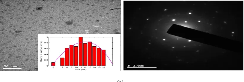
The HRTEM micrographs are shown on the left side of fig.2(a, b and c); obtained for p-Si- nc formed by LP-PLA of p-type Si wafer in double distilled water at different laser power densities of 60 MW/cm2, 84 MW/cm2, and 106 MW/cm2 using Nd:YAG laser beam of λ=1064 nm after 1200 shot each.
5 7 89 10 11 12 13 14 15 16 17 19
0 0.2 0.4 0.6 0.8 1
Size (nm)
N
u
m
b
e
r
o
f
p
a
rt
ic
le
s
(
n
o
rm
(a)
Fig 2 ( left side): HRTEM micrograph for p-silicon ablated nanoparticles in double distilled water by Nd:YAG laser at (a) 60 MW/cm2, (b) 84 MW/cm2 and (c) 106 MW/cm2 respectively. The insets showen at the corners show the histogram distribution of nonocrystal size with least square fit.( right side): The nanocrystals selected area electron diffraction of each sample endicating [111] Si –
crystalline structures.
Close inspection of the micrographs and the size distribution insets asserts that the average sizes of the obtained nano-crystals increased as the laser power increased namely; 5±1.3nm at 60 MW/cm2, 11±4.5 nm at 84 MW/cm2 and 12±4 nm at 106 MW/cm2 laser irradiances. It also shows the size spread increases as the laser power increased.
The right side of fig.(2) reveal the selected area electron diffraction indicating [111] crystalline silicon structure. The lattice structure on fig.(2b) confirmed the same crystalline structure as in the originally used wafers, irrespective of the applied ablating power.
Fig. (3) shows the micrographs of the high resolution transmission electron microscope (HRTEM) for the pn-type Si-nc ablated by Nd-YAG laser irradiance 106 MW/cm2. It turns out that ablated Si-nc from pn-Si wafer has larger mean size ~ 20.63±1.3 nm than those from p-Si wafers formed at the same conditions.
Fig 3: HRTEM micrograph of np-Si nanocystals produced by laser ablation in distilled water (λ=1064nm, Power per pulse 106 MW/cm2). The histogram on the left side shows that the mean crystallite size = 20.63±1.3nm.
The absorption spectra of the different p-Si-nc colloids formed by LP-PLA using different laser irradiances are given in fig.(4a). It is clearly observed that the optical absorption is dependent on the laser irradiance. The absorption spectrum ranging from 350 nm to 800 nm (important region of the solar spectrum) increased 3 times by raising the laser irradiance per pulse from 60 MW/cm2 to 106 MW/cm2. The corresponding mean size of the silicon nanoparticles increased from 5±1.3nm to 12±4 nm at these laser irradiance values, points to their crucial role in raising the corresponding optical absorption spectrum.
Fig.(4b) represent the absorption spectrum for pn-Si nano-crystal formed at laser irradiance 106 MW/cm2 in comparison with p-Si nano-crystal at the same condition. Nearly the same behavior of the optical absorption spectrum is recognized from 500 nm to 800 nm spectral ranges, while higher absorption is clear in the range
5 7 8 91011 1213141516 0
0.2 0.4 0.6 0.8 1
Size (nm)
Nu
m
be
r o
f p
ar
tic
le
s
(n
or
m
)
0 5 10 15 20 25 30 35
0 0.2 0.4 0.6 0.8 1
Size (nm)
N
u
m
b
e
r
o
f
p
a
rt
ic
le
s
(
n
o
rm
from 200 nm to 500 nm spectral ranges indicating that blue shift is recognized for the pn-Si nanocrystals. This result is surely important for solar cell industry.
(a) (b)
Fig 4: (a) optical absorption for p-type nano-crystalline Si colloids prepared at different laser irradiance. (b) Optical absorption for pn-Si nano-crystal colloids compared with p-Si nano crystal formed at the same laser irradiance.
The absorption spectra for pn-Si nano-crystals colloids show a blue shift as clear from fig. (4b) in the range between 200 nm to 500 nm. The absorption data were then analyzed by using the following well-known relation [19] for near edge optical absorption of semiconductors
The energy gap diagram for the pn-Si and p- Si nanoparticles prepared at the same conditions is shown in fig.5.
1 2 3 4 5 6 7
0 100 200 300 400 500 600 700 800 900 1000
h (ev)
(
h
)
2 (
e
v
2 c
m
-2)
pn p
Fig.5: energy gap diagram for pn-Si and p- Si nanoparticles each ablated at 106 MW/cm2. Where the energy gap fro pn-Si is 4.778
eV and for p-Si is 4.437 eV.
The values of the optical band gap as estimated from the intersection of the curves with the energy axis are found to be 4.778 eV and 4.437 eV for the pn-Si and p-Si nanocrystalline semiconductors respectively, prepared by LP-PLA as compared to the well known value of the pn-Si wafer semiconductor [20].
(a) (b)
Fig 6: (a) PL- spectrum for p-type nano-crystalline Si colloids prepared at different laser irradiance. (b) PL spectrum for pn-Si nano crystal compared with p-Si nano-crystal colloids formed at the same laser irradiance 106 MW/cm2.
540 560 580 600 620 640 660 680
Wavelength (nm)
In
te
ns
ity
(
a.
u)
pn-Si p-Si
645 650 655 660 665 670 Wavelength (nm)
In
te
ns
ity
(
a.
The photoluminescence spectra for all Si-nano-crystal colloids shown in in fig. (6a and 6b) exhibits the same photoluminescence line nearly Gaussian profile centered at 652.5±0.5 nm for all the samples. However, in accordance with previous inherent absorption spectra, relatively higher PL spectral intensity is encountered by the pn-type Si- nano-crystal colloids.
IV.
CONCLUSION
It was found that the particle density and the nanocrystals sizes are dependent to the laser
fluencies while the Si-nc structures kept perfect crystalline structure [111] irrespective of the laser
properties and fluencies. The optical absorption and optical luminescence spectra were found to
change as function in the laser beam properties. The result obtain for pn-Si could be interested for
solar cell industry.
V.
ACKNOWLEDGEMENT
The authors acknowledge the assistance of the Laser Physics Lab. team, Faculty of Science, Cairo University. Many thanks are due to the International Arab Optronics Company for providing the silicon wafers. This research was partially funded by Zewail City of Science and Technology.
REFERENCES
[1] R. A. Street, “Technology and Applications of Amorphous Silicon”, Springer, Heidelberg, 2000. [2] "Thin Film Solar Technology Market Shares, Strategies and Forecasts, Worldwide, 2011 to 2017" -
report by U.S. Company, Wintergreen Research http://wintergreenresearch.com/ [3] D. V. Talapin, J.S . Lee, M.V. kovolenko, E. V.Shevchenko, Chem. Rev., 110,389, 2010. [4] H. Liu et ale, Adv. Mater, 23, 3832, 2011.
[5] I. Chung, B. Lee, J. He, R. P. H. Chang, M. G. Kanatzidis, Nature, 485, 486, 2012. [6] I.O. Sosa, C. Noguez, R. G. Barrera, J. Phys. Chem. B, 107, 6269, 2003.
[7] H. H. Wang et ale, Adv. Mater, 18, 491, 2006.
[8] K. L. McGillivray, M. R. Decan, D. Wang, J. C. Scania, J. Amer. Chem. Soc., 128, 5980, 2006. [9] Riad, A. Ismail, et al. Appl. Nanosci., vol.1, p.45, 2011.
[10] V. Svrcek, H. Fujiwara and M. Kondo, Appl. Phys. Lett. 92, 143301, 2008 doi: 10.1063/ 1.2905269. [11] R. Schaller and V. Klimov, Phys. Rev. Lett., 92, 186601, 2004 doi: 10. 1103 / Phys. Rev. Lett. 92. [12] 186601.
[13] M. C. Beard et ale, Nano Lett., 7, 2506, 2007 doi: 10. 1021/ nl. o714861.
[14] K. Grieve, P. Mulvaney, F. Grieser, Curr. Opin, Colloid. Interface Sci, 5, 168, 2000. [15] M. A. El-Sayed, Acc. Chem. Res., 34, 257, 2001.
[16] C. Burda, X. B. Chen, R. Narayanan, M. A. El-Sayed, Chem. Rev., 105, 1025, 2005. [17] Y. N. Xi et ale, Adv. Mater, 15,352, 2003.
[18] R. Jin et al, Nature, 423, 487, 2003.
[19] F. Wang et ale, Inorg. Chem., 45, 7511, 2006.