657 | International Journal of Computer Systems, ISSN-(2394-1065), Vol. 03, Issue 12, December, 2016 The Internet of things (IoT) is the on-going big phase in the evolution of the Internet. For the ease of deployment, IoT devices are often wireless and battery powered. Therefore, the IoT requires a low-power processor to reduce power consumption and ensure a long lifetime. In this study, we designed a low-power processor for the IoT. Its performance is appropriate for the IoT satisfying low-power consumption. The proposed processor has 16-bit and 32-bit Instruction Set Architecture (ISA) and 3-stage pipeline architecture. We demonstrate the feasibility of our processor for IoT by FPGA prototyping and ASIC realization.
Keywords: IoT, Low-power, Processor, SoC
I. INTRODUCTION
The Internet of things (IoT) is becoming increasingly pervasive in areas that include medical care, environment monitoring, and intelligent transportation. In addition, the IoT is a key concept for a smart home. To make its deployment easier, such devices are often wireless and battery powered [1–7]. An important issue is the need for low-power consumption to ensure a long battery life [8–14]. In particular, when implementing a system on a chip (SoC) which integrates multiple hardware blocks into a single chip, it is important to reduce the power consumption due to leakage current problems [15–17]. To keep sensors working for a sufficient period of time without frequent maintenance, most tasks are light and a low-power processor with high energy efficiency is adopted in IoT applications [18]. Low-power processors generally have low performance, but it is possible to increase the performance by deploying additional hardware or improving the hardware architecture [19–22]. In the case of a high-performance processor, increasing the performance increases the power consumption. A high-performance processor can reduce the power consumed by reducing the operation of the processor by applying a hardware accelerator or hardware designed for the purpose of use [23–26]. Therefore, we designed a processor with a focus on low-power consumption for the IoT, and improved the performance by adopting fully pipelined Harvard architecture.
In this paper, we present an IoT processor that was designed to meet the low-power and performance requirements for a mobile IoT. The proposed processor uses a 16 bit and 32 bit instruction set architecture (ISA) and has a 3-stage pipeline, 16 general purpose registers, and a Harvard architecture to increase the performance.
The rest of the paper is organized as follows. In section II, we introduce the architecture of the low power processor including pipeline stages in detail. In section III explains the implementation and verification of the processor with field programmable gate array (FPGA) prototyping and ASIC design. Finally, we conclude this paper in section IV.
II. ARCHITECTURE OF THE LOW-POWER PROCESSOR Our processor adopts 3-stage pipeline to improve the performance efficiency. Unlike the Von Neumann architecture, in which the instructions and data share a single node, the Harvard architecture has a structure in which data nodes and instruction nodes exist separately. This allows the processor to simultaneously access instructions and data, resulting in a higher performance. We adopted the Harvard architecture to achieve a high data processing requirement for IoT.
The proposed design has 16 general purpose registers. The operand values of these registers are used for general operations, with the results also stored at these locations. A portion of these general registers function as a program counter register (PC), link register (LR), and stack pointer register (SP). The address of each register is 4 bit. Registers with addresses ranging from 0x0 to 0x7 can be accessed using 3-bit addresses. These registers are used for operations when 16-bit instruction with a relatively small amount of information needs to be stored. A 32-bit instruction uses every registers from 0x0 to 0xF for the operation.
The pipelines divide an operation of a processor into several stages. Each stage is performed independently, and when an instruction passes to the next stage, the stage that passed the instruction performs its operation on the next instruction. The pipeline stages of proposed processor consist of fetch, decode, and execute and write back. Figure 1 shows the pipeline architecture of the processor.
A. Fetch
Figure 1. Pipeline architecture of the low-power processor
Figure 2. Low-power processor including peripherals read by fetch stage when the second instruction in the
instruction buffer is transferred the next stage. The fetch stage updates the PC value when new instruction is read.
B. Decode
The instruction transferred by the fetch stage contains information such as the address and immediate value of the register used for the operation, command, and destination register address, which indicates the address where to store the result. The instruction is decomposed into the data that used in execute and write back stage. First, the decode stage analyzes the instruction and extracts 6-bit command, including the operands information. The operand type is an immediate or register/immediate or registers only. After obtaining operand information, the operand type is determined by analyzing the immediate value or register address containing in the instruction. The immediate or corresponding register values are transmitted to the execute and write back stage along with the 6-bit command data that defines the operation. At the same time, options for the operation are forwarded to the execute and write back stage. The operands that are required in the execute and write back stage are defined by the 6-bit command. The most instruction has a destination register address for store the result of operation. However, some instruction store the result of operation to the register without indicating the destination register address in the instruction directly. In this case, The decode stage addresses the corresponding destination address for the instruction.
C. Execute and Write Back
In the execute and write back stage, operations are performed using the command and operand data received from the decode stage. And, the result is stored to the destination register. In order to support the instructions, an arithmetic logic unit (ALU), branch, load/store, and push/pup units are implemented. In case of load or pop instructions, the pipeline stalls and one clock cycle for
memory access through advanced high-performance bus (AHB).
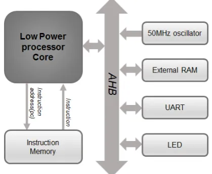
III. IMPLEMENTATION AND VERIFICATION We implemented the proposed processor in Verilog HDL and verified the functionality of the processor with simulation and FPGA prototyping. Figure 2 shows the architecture of our processor along with peripherals including AHB, instruction memory, external RAM, LED controller, RS-232C.
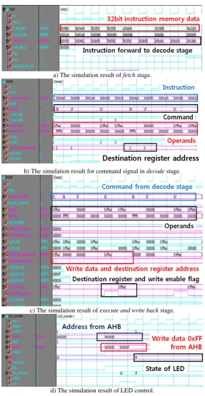
Figure 3 shows the simulation results of the processor using the test program which controls the peripherals. The fetch stage reads the instruction from the program memory and transfers the instruction to decode stage as shown in Fig. 3(a). The decode stage receives the instruction from fetch and decodes the instruction. This instruction is
a) The simulation result of fetch stage.
b) The simulation result for command signal in decode stage.
c) The simulation result of execute and write back stage.
d) The simulation result of LED control.
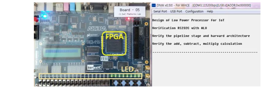
Figure 5. Layout of the low-power processor. Figure 4. photograph of the verification environment and the program running on the processor.
After the simulation, we validated the operation of the processor using a verification environment. A DE2-115 development board is exploited to implement FPGA prototyping for the verification environment which stores the test program in ROM, and operates that program using proposed processor on 50MHz operating frequency. Figure 4 shows the photograph of the verification environment and the program running on the processor. As shown in Fig. 4(a), the LEDs are controlled successfully. Fig. 4(b) shows the firmware running on the processor through a RS-232C channel which provides the way to monitor and control the processor.
Finally, The low-power processor was fabricated by using a Magnachip 0.18 um CMOS technology. A chip photograph of the low-power processor is shown in Fig. 5. The die size of the proposed processor is 3.8×3.8mm2, and the operating frequency of the processor is up to 50MHz. This chip consists of the proposed processor, AHB bus, RS232C, LED controller, instruction memory controller, and RAM controller. In addition, it has 64 KB of internal memory.
IV. CONCLUSIONS
In this paper, we proposed a low-power processor for IoT devices. The low-power processor has a 3-stage pipeline and Harvard architecture. ISA has 16-bit and 32-bit instructions. The processor was implemented on FPGA and verification results confirms the functionality of the processor. Moreover, the processor was fabricated by using the Magnachip 0.18 um CMOS technology.
ACKNOWLEDGEMENT
This study was supported by the Research Program funded by the Seoul National University of Science and Technology (2015-1239).
REFERENCES
[1] A. Engel, A. Koch "Heterogeneous Wireless Sensor Nodes that Target the Internet of Things", IEEE Micro, vol. 36, no. 6, pp. 8-15, Dec. 2016
[2] V. J. Reddi, H. Kim "On the Internet of Things", IEEE Micro, vol 36, no 6, pp. 5-7, Dec 2016
[3] S. M. Lee, J. W. Shin, O. S. Gwon, and S. E. Lee, “3D Interaction Glove: Virtual and Physical Space Realization Through Data
Glove”, International Journal of Applied Engineering Research
(IJAER), vol.10, no.17, pp.38354-38357, Oct. 2015
[4] Y. S. Jeong, Y. J. Kwon, and S. E. Lee, “Implementation of Smart U-Health Care System”, Information Journal, vol.17, no.10(A), pp.4911-49916, Oct. 2014.
[5] H. M. Choi, Y. S. Jeong, S. J. Son, J. G. Son, and S. E. Lee, “IPFM: Intelligent Pressure Foot-Mouse”, International Journal of Multimedia and Ubiquitous Engineering, vol.8, no.5, pp. 31-40, Sep., 2013.
[6] M. Ambrosin, A. Anzanpour, M. Conti, "On the Feasibility of Attribute-Based Encryption on Internet of Things Devices", IEEE Micro, vol. 36, no. 6, pp. 25-30, Dec. 2016
[7] F. Jalali, A. Vishwanath, J. D. Hoog, F. Suits, “Interconnecting Fog Computing and Microgrids for Greening IoT”, Innovative Smart Grid Technologies - Asia (ISGT-Asia), 2016 IEEE, Dec. 2016 [8] H. Tamura, K. Kato, T. Ishizu, W. Uesugi, A. Isobe, N. Tsutsui, Y.
Suzuki, Y. Okazaki, Y. Maehashi, J. Koyama, Y. Yamamoto, S. Yamazaki, M. Fujita, J. Myers, P. Korpinen, "Embedded SRAM and Cortex-M0 Core Using a 60-nm Crystalline Oxide Semiconductor", IEEE Micro, vol. 34, no. 6, pp. 42-53, Dec. 2014 [9] K. Ma, X. Li, S. Li, Y. Liu, J. J. Sampson, Y. Xie, V. Narayanan,
"Nonvolatile Processor Architecture Exploration for Energy-Harvesting Applications", IEEE Micro, vol 35, no. 5, pp. 32-40, Oct. 2015
[10] H. Tamura, K. Kato, T. Ishizu, W. Uesugi, A. Isobe, N. Tsutsui, Y. Suzuki, Y. Okazaki, Y. Maehashi, J. Koyama, Y. Yamamoto, S. Yamazaki, M. Fujita, J. Myers, P. Korpinen, "Embedded SRAM and Cortex-M0 Core with Backup Circuits using a 60-nm Crystalline Oxide Semiconductor for Power Gating", IEEE Micro, Jan 2015
[11] K. Ma, X. Li, S. Li, Y. Liu, J. J. Sampson, Y. Xie, V. Narayanan, "Nonvolatile Processor Architecture Exploration for Energy-Harvesting Applications", IEEE Micro, vol 35, no. 5, pp. 32-40, Oct. 2015
Nagai, S. Sasagawa, D. Ito, Y. Hata, T. Hamada, R. Arasawa, K. Hanaoka, M. Sakakura, H. Suzawa, Y. Yamamoto, S. Yamazaki, "Scaling to 50-nm C-axis aligned crystalline In-Ga-Zn oxide FET with surrounded channel structure and its application for less-than-5-nsec writing speed memory", VLSI Technology Digest of Technical Papers, 2014 Symposium, Jun 2014
[17] S. D. Kim and S. E. Lee, “Little Core Based System on Chip Platform for Internet of Thing” Int. J. Electr. Comput. Eng. (IJECE), vol. 5, no. 4, pp. 695–700, Aug. 2015.
[18] S. Izumi, K. Yamashita, M. Nakano, H. Kawaguchi, H. Kimura, K. Marumoto, T. Fuchikami, Y. Fujimori, H. Nakajima, T. Shiga, M. Yoshimoto, "A Wearable Healthcare System With a 13.7μ A Nois Tolerant ECG Processor" IEEE Trans. on Biomed. Circuits Syst., vol. 9, no. 5, pp. 733–742, Oct 2015.
[19] S. M. Lee, J. H. Jang, S. M. Lee, J. H. Oh, and S. E. Lee, “Design of a DMA Controller for Loss-less Image Processing”, J.ournal of Integrated Circuits and Systems (JICAS), vol. 3, no. 1, pp. 1–6, 2016.
[20] S. D. Kim and S. E. Lee, “An ARM Cortex-M0 Based FPGA
Platform in Teaching Computer Architecture”, International Journal
of Computer and Information Technology, Vol. 4, No. 6, pp.939-941, Nov. 2015.
[21] S. D. Kim and S. E. Lee, “A Scalable Large Format Display Based
on Zero Client Processor” International Journal of Electrical and
Computer Engineering (IJECE), vol. 5, no. 4, pp. 714–719, Aug. 2015.
[22] S. D. Kim and S. E. Lee, “Architecture for A Zero Client Based
Scalable Large Format Display System”, International Journal of
Computer and Information Technology, vol. 04, no. 03, pp. 540– 542, May. 2015.
[23] O. S. Gwon, J. K. Kim, J. W. Shin, and S. E. Lee, “Live Demonstration : AHB based Digital Filter for Low Power Mobile
Healthcare System”, 13th IEEE Asia Pacific Conference on Circuits
and Systems (APCCAS 2016), Jeju, Korea, Oct. 2016.
[24] J. K. Kim, O. S. Gwon, and S. E. Lee, “Design of an Area-Efficient Hardware Filter for Embedded System", 13th International SoC Design Conference (ISOCC 2016), Jeju, Oct. 2016.
[25] S. E. Lee and Y.-M. Jeong, “A 32-bit High Performance VLIW
DSP for Software Defined Radio Applications”, IEICE
Transactions on Electronics, vol. E87-C, no. 11, Nov. 2004. [26] R. Puri, M. Choudhury, H. Qian, M. Ziegler, "Bridging high