965 | P a g e
SIMULATION OF A THREE LEVEL BOOSTING PFC
EMISSION WITH SENSORLESS ELECTRICAL
DEVICE VOLTAGE RECONCILIATION
MANAGEMENT
Machunoori Mounica
1, CH Suneetha K
2 1,2Assistant Professor, GRIET Hyderabad
ABSTRACT
Compared with the conventional boosting PFC converter, the three-level boosting PFC converter has two cascaded switches and two cascaded capacitors across the dc-side voltage. Two capacitor voltages may be different due to their mismatched equivalent series resistance, their mismatched capacitance, and the mismatched conducting time of the corresponding switches. It follows that the controller needs to sense the capacitor voltages to balance both capacitor voltages. In this paper, the sensorless capacitor voltage balancing control (SCVBC) without sensing the capacitor voltages is proposed, and the total number of the feedback signals is saved. The proposed SCVBC is digitally implemented in an FPGA-based system. The provided simulated and experimental results also demonstrate the proposed SCVBC.
I. INTRODUCTION
To reduce the power transmission loss and increase the system stability, more and more power-electronics products are forced to include the power factor correction (PFC) function. Generally speaking, the PFC function includes shaping the ac-side current waveform and regulating the dc-side voltage. Due to the characteristics of the continuous current, the boost-derived PFC converters have been widely used to achieve the desired PFC function. For the conventional boost dc/dc converter, the single switch needs to withstand the dc output voltage when the single switch blocks. Two cascaded switches and two cascaded capacitors are connected together in the three-level boosting dc/dc converter. When one of the switches conducts and the other blocks, the blocking switch needs to withstand only half dc output voltage if both capacitor voltages are balanced. If not balanced, one of the capacitor voltages may be larger than the breakdown voltage of the switch, which would contribute to make damage to the switch. It is noted that the inductor voltage in the three-level boost dc/dc converter has three levels, which makes the three-level boosting dc/dc converter to have smaller inductor current ripple
966 | P a g e
the interleaved PWM scheme was first proposed to control the three-level boosting PFC converter. the multiloop control includes the feed forward loop, the inner current loop, and the outer voltage loop. The three single-phase three-level boosting PFC converter in Delta connection is used to achieve the three-phase PFC function with the ability of redundancy. However, the balance between two capacitor voltages should be noted. In practice, the mismatched capacitances and the mismatched equivalent series resistance (ESR) would result in the voltage imbalance. Therefore, the control of the three-level boosting converter needs to balance both capacitor voltages. In the literature, the voltage balancing control loop for three-level boosting converters can be found. In fact, the other voltage balancing control can be found in the controls of the half-bridge PFC converter and the multilevel inverter. All the methods need to sense capacitor voltages to detect the voltage imbalance and yield the desired voltage balancing function. The multiloop interleaved control with conventional capacitor voltage balancing control (CVBC). One control signal is generated by the multiloop control, and the other control signal is yielded by CVBC with sensing the capacitor voltages. For the three-level boosting dc/dc converter, a voltage balancing control method with sensing only inductor current was first proposed in. In this paper, the concept in is extended to the three-level boosting PFC application and the proposed controller is named the sensorless capacitor voltage balancing control (SCVBC). The voltage imbalance between two capacitor voltages is skillfully detected by sensing the inductor current. The detailed analysis and the design rule of the proportion-type voltage balance controller are also provided. It follows that sensing individual capacitor voltage is not
Required, and at least one voltage sensor is saved. The provided simulation and experimental results show the effectiveness of the proposed SCVBC.
II. LITERATURE SURVEY
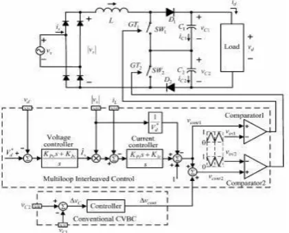
The input ac voltage vs = Vˆs sin(2πft) is assumed to be a sinusoidal function with a peak amplitude Vˆs . Through
the diode rectifier, the input voltage of the three-level boosting converter can be expressed with the rectified voltage |vs |. By assuming that the switching frequency fs is much larger than the line frequency f, the control signals vcont1 and vcont2 can be regarded as two constants within the switching period Ts = 1/fs . In addition, the ideal inductor and the ideal capacitors are assumed. That is, the inductor resistance and the capacitor resistances are assumed to be zero. In Fig. 1, two triangular signals vtri1 and vtri2 are interleaved by 180◦ . The conventional multiloop control generates the control signal vcont1 , and then, the gate signal GT1 is generated from the comparison of the control signal vcont1 and the triangular signal vtri1 . After sensing both capacitor voltages, the voltage imbalance is detected and the conventional CVBC generates the compensation signal Δvcont. Then, the other control signal vcont2 is obtained by adding the compensation signal Δvcont to the control
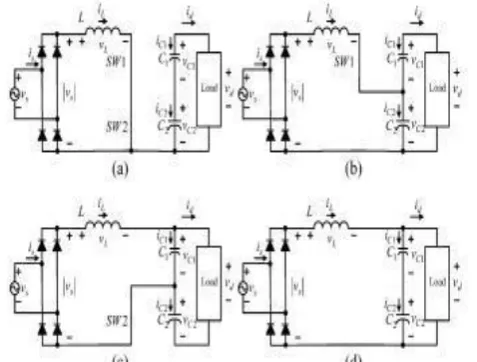
signal vcont1 . The gate signal GT2 is obtained from the comparison of the control signal vcont2 and the triangular signals vtri2 . Due to the input inductor L and two diodes D1 and D2 in the three-level boosting PFC converter, both switches can be conducting at the same time without the concern of the shortcircuit damage. As plotted in Fig. 2, there are four switching states in the three-level boosting PFC converter. As shown in Fig. 2(a), both switches turn ON in the switching state 1. Thus, the inductor voltage vL in the three-level.
967 | P a g e
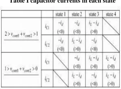
Table I capacitor currents in each state
boosting PFC converter equals the rectified input voltage
vL = |vs | and both capacitors supply energy to the load iC 1 = iC 2 = (−id ) < 0. In the switching state 2 in Fig. 2(b),
the top switch turns ON and the bottom switch turns OFF. The resulting inductor voltage vL equals the rectified input voltage |vs | minus the bottom capacitor voltage vL = |vs | − vC 2 . Additionally, the capacitor C1 supplies energy to the load iC 1 = (−id ) < 0, but the capacitor C2
stores the energy from the input voltage iC 2 = (iL − id ) > 0. Similarly, the resulting inductor voltage in Fig. 2(c)
equals the rectified input voltage minus the top capacitor voltage vL = |vs | − vC 1. In the switching state 3, the top capacitor C1 is charged iC 1 = (iL − id ) > 0, but the bottom capacitor C2 is discharged iC 2 = (−id ) < 0. When
both switches turn OFF in Fig. 2(d), the resulting inductor
voltage equals the rectified input voltage minus the output voltage vL = |vs | − vd = |vs | − vC 1 − vC 2. The rectified
input voltage |vs |supplies the load current and charges both capacitors simultaneously iC 1 = iC 2 = (iL − id ) > 0. All the capacitor currents in various switching states are tabulated in Table I. The behavior of the three-level boosting converter can be divided into two cases as shown in Fig. 3. In the case of 2 > vcont1 + vcont2 > 1, two switches may conduct at the same time within the switching period Ts and there are switching state 1, state 2, and state 3. In the other case of 1 > vcont1 + vcont2 > 0, only switching state 2, state 3, and state 4 exist.
III. PROPOSED METHOD AND RESULTS
The multiloop interleaved control and the proposed SCVBC with the proposed sampling/hold strategy are where only the input voltage vs , the output voltage vd , and the inductor current iL are sensed. It is noted that the proposed sampling/hold strategy samples the inductor current iL thrice per switching period Ts , and obtains the average value IL and the other two values IvC 1 and IvC 2
. The average value current IL is input to the multiloop
control to yield the desired PFC function and obtain the control signal vcont1 . The difference ΔIvC between two
values IvC 1 and IvC 2 is calculated and the compensating signal Δvcont is obtained by the used P controller
968 | P a g e
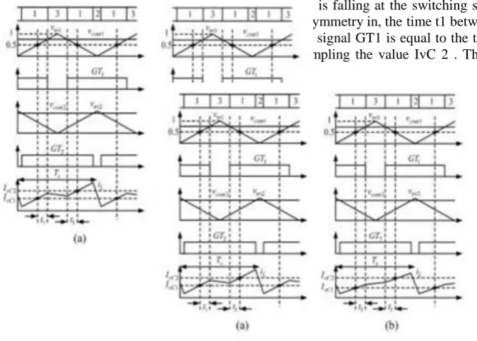
Fig. 7. Illustrated waveforms(2 > vcont1 + vcont2 > 1). (a) vC 1 > vC 2 > |vs | and (b) vC 1 > |vs | > vC 2 . value is defined as IvC 1 . The value IvC 2 is sampled when the triangular signal vtri1 falls to 0.5 from the peak. After finishing all the sampling actions, the multiloop control is performed at the controller time, and updates the two control signals at the valley of the triangular signal vtri1 . In the following paragraphs, the analysis is divided into two cases - 2 > vcont1 + vcont2 > 1 and 1 > vcont1 + vcont2 > 0
2 > vcont1 + vcont2 > 1. The illustrated waveforms for the voltage imbalance ΔvC
> 0 (i.e., vC 1 > vC 2 ) are plotted in. Since the input ac voltage vs is time-varying, the voltage imbalance ΔvC > 0
may be divided into two conditions—either vC 1 > vC 2 > |vs | or vC 1 > |vs | > vC 2 . The waveforms in the condition vC 1 > vC 2 > |vs | are plotted in, and the inductor current iL is falling at the switching state 2. But the inductor current iL is rising at the switching state 2 in the other condition vC 1 > |vs | > vC 2 as plotted in. The illustrated waveforms for the voltage imbalance vC 2 > vC 1 > |vs | and vC 2 > |vs | > vC 1 are plotted in respectively. It is noted that in, the inductor current iL is falling at the switching state 3, but the current iL is rising at the switching state 3 in. Due to the waveform symmetry in, the time t1 between the instants of sampling the value IvC 1 and the turning-off instants of the gate signal GT1 is equal to the time between the turning-on instants of the gate signal GT1 and the instants of sampling the value IvC 2 . Therefore, the time t1 can be expressed in terms of the control signal vcont1
969 | P a g e
Substituting (8) and (10) into (11) obtains
By substituting (6) into (12), the expression ΔIvC in (12) can be rewritten as
Because the coefficient k1 is always positive, the difference ΔIvC is proportional to the voltage imbalance (vC 2 − vC 1 ). It follows that the difference ΔIvC can be
used to detect the voltage imbalance (vC 2 − vC 1 ) without directly sensing the capacitor voltages. 1 > vcont1 + vcont2 > 0
970 | P a g e
Illustrated waveforms (1 > vcont1 + vcont2 > 0). (a) |vs | > vC 2 > vC 1 and (b) vC 2 > |vs | > vC 1. In this case, the illustrated waveforms for the voltage imbalance vC 1 > vC 2 > |vs | and vC 1 > vC 2 > |vs | are plotted respectively. In the inductor current iL is rising at the switching state 3, but the inductor current iL is falling at the switching state 3. The illustrated waveforms for the voltage imbalance |vs | > vC 2 > vC 1 and vC 2 > |vs | > vC 1 are plotted respectively. It is noted that in the inductor current iL is rising at the switching state 2 due to |vs | > vC 2 , but the current iL is falling at the switching state 2 in due to vC 2 > |vs |. Due to the symmetry, the time t2 between the instants of sampling the value IvC 1 and the turning-off instants of the gate signal GT1 can be expressed in terms of the control signal vcont1
the conducting times for switching state 2 and switching state 3 are (vcont1Ts ) and (vcont2Ts ), respectively. The remaining times in a switching period Ts for switching state 4 is(1 − vcont1 − vcont2 )Ts. The average inductor voltage vL T s in the three-level converters is the same as (9), equation (15), the difference ΔIvC between two sampled values IvC 1 and IvC 2 can expressed in terms of the time
The coefficient k2 may be either positive one or negative one. In order to force the coefficient k2 positive, the denominator should be positive
971 | P a g e
Where vC 2, max is the maximum bottom capacitor voltage. Then, the difference ΔIvC would be proportional to the voltage imbalance (vC 2 − vC 1). From (13) and (18) in both cases, the difference ΔIvC in both cases are proportional to the voltage imbalance (vC 2 − vC 1 ) via
properly selecting the controller parameter KP , which implies that the difference ΔIvC obtained from the proposed SCVBC can be used to detect the voltage imbalance (vC 2 − vC 1 ) without directly sensing the capacitor voltages.
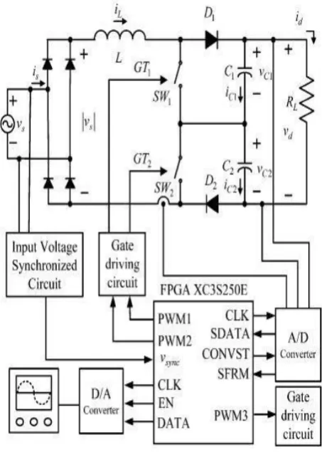
Fig. 16. Block diagram of the implemented three-level boosting PFC converter
IV. CONCLUSION
In this paper, the SCVBC method for the three-level boosting PFC converter has been proposed. The proposed method shows that the voltage imbalance can be detected from sensing the inductor current by the proposed sampling/hold strategy. That is, it eliminates the need for extra sensors, reduces control complexity, and reduces the cost and size. The reduction of cost and size are the important contributions for PFC converters. The control method is implemented in an FPGA-based system, and all the provided results demonstrate the proposed method.
REFERENCES
[1] B. Singh, B. N. Singh, A. Chandra, K. Al-Haddad, A. Pandey, and D. P. Kothari, ―A review of single-phase improved power quality ACDC converters,‖ IEEE Trans. Ind. Electron., vol. 50, no. 5, pp. 962–981, Oct. 2003. [2] J. C. Crebier, B. Revol, and J. P. Ferrieux, ―Boost-chopper-derived PFC rectifiers: Interest and reality,‖ IEEE Trans.
Ind. Electron., vol. 52, no. 1, pp. 36–45, Feb. 2005.
[3] L. S. Yang, T. J. Liang, H. C. Lee, and J. F. Chen, ―Novel high step-up DC–DC converter with coupled-inductor and voltage-doubler circuits,‖ IEEE Trans. Ind. Electron., vol. 58, no. 9, pp. 4196–4206, Sep. 2011.
972 | P a g e [5] M. H. Todorovic, L. Palma, and P. N. Enjeti, ―Design of a wide input range DC–DC converter with a robust power
control scheme suitable for fuel cell power conversion,‖ IEEE Trans. Ind. Electron., vol. 55, no. 3, pp. 1247–1255, Mar. 2008.
[6] W. Li and X. He, ―Review of nonisolated high-step-Up DC/DC converters in photovoltaic grid-connected applications,‖IEEE Trans. Ind. Electron., vol. 58, no. 4, pp. 1239–1250, Apr.2011.
[7] J. M. Kwon, B. H. Kwon, and K. H. Nam, ―Three-phase photovoltaic system with three-level boosting MPPT control,‖IEEE Trans. Power Electron., vol. 23, no. 5, pp. 2319–2327,Sep. 2008.
[8] V. Yaramasu and B.Wu, ―Three-level boost converter based medium voltage megawatt PMSG wind energy conversion systems,‖ in Proc. Energy Convers. Cong. Expo., 2011, pp. 561–567.
[9] M. T. Zhang, Y. Jiang, F. C. Lee, and M. M. Jovanovic, ―Single-phase three-level boost power factor correction converter,‖ in IEEE App. Power Electron. Conf., 1995, pp. 434–439.
[10] J. R. Pinheiro, D. L. R. Vidor, and H. A. Grundling, ―Dual output threelevel boost power factor correction converter with unbalanced loads,‖ in Proc. IEEE Power Electron. Spec. Conf., 1996, pp. 733–739.
[11] B. R. Lin and H. H. Lu, ―A novel PWM scheme for single-phase threelevel power-factor-correction circuit,‖ IEEE
Trans.Ind. Electron., vol. 47, no. 2, pp. 245–252, Apr. 2000.
[12] H.Wu and X. He, ―Single phase three-level power factor correction circuit with passive lossless snubber,‖ IEEE
Trans.Power Electron., vol. 17, no. 6, pp. 946–953, Nov. 2002.
[13] J. Y. Liao and H. C. Chen, ―Multiloop interleaved control for two -switch two-capacitor three-level SMR without capacitor voltage balancing loop,‖ in Proc. IEEE Energy Convers. Congr.Expo., 2011, pp. 3766–3772.
[14] R. Greul, S. D. Round, and J. W. Kolar, ―The Delta-Rectifier: Analysis, Control and Operation,‖ IEEE Trans. Power
Electron., vol. 21, no. 6, pp. 1637–1648, Nov. 2006.
[15] E. Ribeiro, A. J. M. Cardoso, andC.Boccaletti, ―Fault-tolerant strategy for a photovoltaic DC–DC converter,‖ IEEE
Trans. Power Electron., vol. 28, no. 6, pp. 3008–3018, Jun.2013.
[16] R. Ghosh and G. Narayanan, ―A simple analog controller for single phase half-bridge rectifier,‖ IEEE Trans. Power
Electron., vol. 22, no. 1, pp. 186–198, Jan. 2007.
[17] B. R. Lin, T. L. Huang, and C. H. Huang, ―Bi-directional single-phase half-bridge rectifier for power quality compensation,‖ IEE, Electric Power Appl., vol. 150, no. 4, pp. 397–406, July 2003.
[18] Z. Shu, N. Ding, J. Chen, H. Zhu, and X. He, ―Multilevel SVPWM with DC-link capacitor voltage balancing control for diode-clamped multilevel converter based STATCOM,‖ IEEE Trans. Ind. Electron., vol. 60, no. 5, pp. 1884–1896, May 2013.