University of New Orleans
University of New Orleans
ScholarWorks@UNO
ScholarWorks@UNO
University of New Orleans Theses and
Dissertations
Dissertations and Theses
12-17-2010
Implementation of Separable & Steerable Gaussian Smoothers on
Implementation of Separable & Steerable Gaussian Smoothers on
an FPGA
an FPGA
Arjun Joginipelly
University of New Orleans
Follow this and additional works at: https://scholarworks.uno.edu/td
Recommended Citation
Recommended Citation
Joginipelly, Arjun, "Implementation of Separable & Steerable Gaussian Smoothers on an FPGA" (2010). University of New Orleans Theses and Dissertations. 98.
https://scholarworks.uno.edu/td/98
This Thesis-Restricted is protected by copyright and/or related rights. It has been brought to you by
ScholarWorks@UNO with permission from the rights-holder(s). You are free to use this Thesis-Restricted in any way that is permitted by the copyright and related rights legislation that applies to your use. For other uses you need to obtain permission from the rights-holder(s) directly, unless additional rights are indicated by a Creative Commons license in the record and/or on the work itself.
Implementation of Separable & Steerable Gaussian Smoothers on an FPGA
A Thesis
Submitted to the Graduate Faculty of the
University of New Orleans
in partial fulfillment of the
requirements for the degree of
Master of Science
in
Engineering
Electrical
by
Arjun Kumar Joginipelly
B.S, JNTU University, 2007
ii
Dedication
iii
Acknowledgements
I would like to thank Dr. Dimitrios Charalampidis, my advisor, for his help, suggestions and
guidance throughout the course of my thesis research. I appreciate his direction, supervision of
my work and his patience especially for reading, rereading and editing my thesis which helped
me in progressing in the right path.
I acknowledge my friend Mr. Rajesh Chary for his support throughout my studies without which
it would have been impossible for me to get through my Master’s degree. His patience,
assistance and insight served as invaluable assets in both my personal and academic life.
I would also like to thank to Dr. Vesselin Jilkov and Dr. George Ioup for their willingness to
serve as members in my thesis committee.
Most importantly, I would like to thank my parents for teaching me study habits and the value of
education. I am indebted to them for their encouragement in my childhood years to constantly
strive for a successful career.
And last, but certainly not least, I would like to express my warmest regards and gratitude to my
grandfather for inspiring me from an early age to commit myself to helping others.
iv
Glossary of Abbreviations
FPGA – Field Programmable Gate Arrays
PLD – Programmable Logic Device
ASIC – Application Specific Integrated Circuit
FSM – Finite State Machine
DSP – Digital Signal Processor
VHDL – Very High speed integrated Description Language
ISE – Integrated Software Environment
DSF – Directional Smoothing Filter
LB – Logic Block
LUT – Look up Table
BRAM – Block RAM
IP – Intellectual Property
v
Table of Contents
List of Tables ... vii
List of Figures ... viii
Abstract ... ix
Chapter 1 ...1
1.1 Introduction ...1
1.2 Research Objectives ...2
1.3 Scope of Thesis ...3
1.4 Organization of Thesis ...3
Chapter 2 ...4
2.1 Field Programmable Gate Array (FPGA) ...4
2.2 Xilinx VirtexII Pro FPGA Platform ...6
Chapter 3 ...9
3.1 Design Language ...9
3.1.1 Verilog Hardware Design Language ...11
3.1.2 VHSIC Hardware Design Language (VHDL) ...12
3.2 Software Tools ...12
3.3 Other languages and Tools ...13
Chapter 4 ...14
4.1 Convolution...14
4.2 Gaussian Mask ...16
vi
Chapter 5 ...21
5.1 Hardware Implementation ...21
5.2 Proposed Design Methodology ...22
5.2.1 General 2D Convolution Method...24
5.2.2 Separable Convolution Method 1 using multiple BRAMs ...28
5.2.3 Separable Convolution Method 2 using FIFO ...33
5.2.4 Comparisons of Convolution Methods ...38
5.2.5 Extension of Separable Convolution Method 2 using FIFO ...39
5.3 Proposed Steerable Concept Implementation ...43
Chapter 6 ...47
6.1 Summary and Conclusions ...47
6.2 Limitations ...48
6.3 Future Work ...48
Bibliography ...49
Appendix ...53
vii
List of Tables
Table 5.1: A 7×7 Test Image
Table 5.1: A 3×3 Gaussian Mask with Mean = 0, σ = 1 and N = 0.0016
Table 5.3: Device Utilization Summary of Two Dimensional Convolution Method
Table 5.4: Horizontal Gaussian Mask with Mean = 0, σ = 1 and N = 0.0016
Table 5.5: Vertical Gaussian Mask with Mean = 0, σ = 1 and N = 0.0016
Table 5.6: Device Utilization Summary of Separable Convolution Method 1
Table 5.7: Horizontal Gaussian Mask with Mean = 0, σ = 1 and N = 0.0016
Table 5.8: Vertical Gaussian Mask with Mean = 0, σ = 1 and N = 0.0016
Table 5.9: Device Utilization Summary of Separable Convolution Method 2
Table 5.10: Comparison of Convolution Methods
Table 5.11: Horizontal Gaussian Mask with Mean = 0, σ = 1 and N = 0.0016
Table 5.12: Vertical Gaussian Mask with Mean = 0, σ = 1 and N = 0.0016
Table 5.13: Device Utilization Summary of Separable Convolution Method 2 extended to 48×48
image size and Gaussian mask of 9×1 and 1×9
Table 5.14: Horizontal Gaussian Mask with Mean = 0, σ
x= 3, σ
y= 5, N = 0.001
Table 5.15: Vertical Gaussian Mask with Mean = 0, σ
x= 3, σ
y= 5, N = 0.001
viii
List of Figures
Figure 2.1: Architecture of a generic FPGA ... 4
Figure 2.2: Architecture of Logic Block with one 4-input LUT ...5
Figure 2.3: Block Diagram of XUP VirtexII Pro FPGA Board ...7
Figure 2.4: Picture of XUP VirtexII Pro FPGA Board ... 8
Figure 3.1: Hardware Design Flow ...10
Figure 3.2: Software Design Flow ... 11
Figure 4.1: 2 D Convolution Operation ... 15
Figure 4.1: 2 D Gaussian Mask... 17
Figure 5.1: Block Diagram of Two Dimensional Convolution Method ... 24
Figure 5.2: Schematic Diagram of Two Dimensional Convolution Method ... 25
Figure 5.3: Simulation Results of Two Dimensional Convolution Method ... 26
Figure 5.4: Block Diagram of Separable Convolution Method 1 ...29
Figure 5.5: Schematic Diagram of Separable Convolution Method 1 ...30
Figure 5.6: Simulation Results of Separable Convolution Method 1 ... 31
Figure 5.7: Block Diagram of Separable Convolution Method 2 ... 34
Figure 5.8: Schematic Diagram of Separable Convolution Method 2 ...35
Figure 5.9: Simulation Results of Separable Convolution Method 2 ... 36
Figure 5.10: Schematic Diagram of Separable Convolution Method 2 extended
to a 48×48 image and a Gaussian masks of 9×1 and 1×9 ... 40
Figure 5.11: Simulation Results of Separable Convolution Method 2 extended
to a 48×48 image and a Gaussian masks of 9×1 and 1×9 ... 41
Figure 5.12: Block Diagram of Steerable Implementation ... 44
ix
Abstract
Smoothing filters have been extensively used for noise removal and image restoration.
Directional filters are widely used in computer vision and image processing tasks such as motion
analysis, edge detection, line parameter estimation and texture analysis. It is practically
impossible to tune the filters to all possible positions and orientations in real time due to huge
computation requirement. The efficient way is to design a few basis filters, and express the
output of a directional filter as a weighted sum of the basis filter outputs. Directional filters
having these properties are called “Steerable Filters”. This thesis work emphasis is on the
implementation of proposed computationally efficient separable and steerable Gaussian
smoothers on a Xilinx VirtexII Pro FPGA platform. FPGAs are Field Programmable Gate Arrays
which consist of a collection of logic blocks including lookup tables, flip flops and some amount
of Random Access Memory. All blocks are wired together using an array of interconnects. The
proposed technique [2] is implemented on a FPGA hardware taking the advantage of parallelism
and pipelining.
Keywords
1
CHAPTER 1
Introduction
1.1
Introduction
Current developments of computer systems tend to reduce the size of the hardware. This is a
conclusion drawn from Moore’s law [1]. The hardware specifications and capabilities of a small
laptop ten years ago are comparable to today’s mobile devices, such as the IPhone 3GS. As a
result, embedded computer systems are also becoming increasingly pervasive. For instance,
today’s cars include embedded systems to monitor a wide range of multi-media features such as
audio, video, voice control, and navigation [22]. Another area where embedded systems play an
important role is digital image processing with applications such as automated surveillance
systems [23], traffic light controller systems [24]. In earlier times, those systems were mostly
built with Application Specific Integrated Circuits (ASICs) which are not reprogrammable (or
reconfigurable). A malfunction in one ASIC often results in a complete replacement of the faulty
component. The ASICs lack of flexibility to be reprogrammed is promoting their counterpart,
namely the FPGA (Field Programmable Gate Array) chips.
2
Today, FPGAs can be developed to implement parallel design methodologies, which is not
possible in dedicated DSP designs. ASICs were traditionally preferred over FPGAs because of
their speed, lower power consumption, and higher functionality. However, the improvements on
FPGA technology in recent years have almost closed this gap. ASIC design methods can also be
used for FPGA design, facilitating gate level implementations, thereby decreasing development
time and time-to-market. However, engineers usually use a hardware language, which allows for
a design methodology similar to software design. Maintenance can be performed when an error
is found in the implemented design, since the FPGA fabric can always be reconfigured. This
software view of hardware design allows for a lower overall support requirements, lower cost,
and design abstraction.
The key advantages of FPGAs when compared to DSP implementations include performance,
integration and customization using parallel and pipeline design techniques. Due to the support
of parallelism, FPGAs may be able to achieve huge gains in performance compared to DSP
implementations.
1.2
Research Objectives
3
1.3
Scope of Thesis
The main contribution in this thesis is the design and implementation of directional Gaussian
smoothers [2] on FPGA. Firstly, derivations are presented to show that Gaussian filters are
separable. Secondly, in [13], it was shown that these filters can also be made approximately
steerable. The inferred equations are also derived and presented here for completeness. The
functionality of directional (or steerable) Gaussian smoothers is examined using Matlab
simulations. Then, a VHDL model is developed for a test image of 7×7 and a Gaussian mask of
3×3. Based on the simulation results and logic utilization, we implemented the convolution
operation similar to the techniques presented in [15], [17]. Furthermore, additional techniques
were implemented to improve logic utilization and processing speed for performing convolution.
All the hardware architectural models are prototyped on XC2VP30FFG896, a device technology
of Xilinx VirtexII-Pro FPGA platform. For all methods implemented on the target device,
comparisons are made using logic utilization (in terms of number of flip-flops and slice count)
and number of clock cycles per pixel.
1.4
Organization of Thesis
4
CHAPTER 2
FPGA and Xilinx VirtexII Pro Board
2.1
Field Programmable Gate Array (FPGA)
An FPGA is a chip that allows the user to control and reprogram the functionality of its logic
circuits. All FPGAs consist of three major components, namely Logic Blocks (LB), I/O Blocks,
and Programmable Routing or Interconnect as shown in figure 2.1 [3].
5
In order to implement a circuit on an FPGA, each LB is programmed to perform a small part of
the logic and each I/O block is programmed to act as input or output, as required by the circuit.
The programmable routing is also configured to make all necessary connections between LBs
and from LBs to I/O blocks.
The processing power of an FPGA is directly proportional to the processing capabilities of its
LBs and the total number of LBs available in the array. Currently, most of the commercial
FPGAs use LBs that contain one or more Look-up Tables (LUTs), typically a input LUT. A
4-input LUT can implement any binary function of 4 logic 4-inputs. The architecture of a simple LB
containing one 4-input LUT and one flip-flop for storage is shown in figure 2.2 [3].
6
Modern FPGAs also contain blocks of on-chip memory as well. For example, the target FPGA
device XU2VP30 used in this thesis work contains 136 blocks of 4Kbits of RAM, 13696 slices,
27392 LUTs, 136 18×18 embedded multipliers and 556 bonded IOB’s. An overview and detailed
explanation of target device used is presented in next subheading.
2.2
Xilinx VirtexII Pro FPGA Platform
The XU2VP30-FFG896 is a Xilinx manufactured Virtex-2 Evaluation Board with an advanced
hardware platform that consists of high performance VirtexII Pro Platform FPGA [9],
surrounded by peripheral components that can be used to create a complex system. Main features
of the platform are the following:
Virtex®-II Pro FPGA with PowerPC® 405 cores
Maximum 2 GB of Double Data Rate (DDR) SDRAM
Compact Flash connector
Embedded Platform Cable USB configuration port
Programmable Configuration PROM
On-board 10/100 Ethernet PHY device
RS-232 DB9 serial port
Two PS-2 serial ports
Four LEDs connected to Virtex-II Pro I/O pins
Four switches connected to Virtex-II Pro I/O pins
Five push buttons connected to Virtex-II Pro I/O pins
Six expansion connectors joined to 80 Virtex-II Pro I/O pins
7
AC-97 audio CODEC with audio amplifier and speaker/headphone output
Microphone and line level audio input
On-board XSGA output, up to 1200 x 1600 at 70 Hz refresh
Three Serial ATA ports, two Host ports and one Target port
Off-board expansion MGT link, with user-supplied clock
100 MHz system clock, 75 MHz SATA clock
Provision for user-supplied clock
On-board power supplies
Power-on reset circuitry
PowerPC 405 reset circuitry
The block diagram of the board is shown in figure 2.3.
8
The picture of the board can be seen in figure 2.4 below.
9
CHAPTER 3
Design Language & Software Tools
3.1
Design Language
10
11
Figure 3.2: Software Design Flow
The following subsections discuss the two common high level hardware design languages
(HDLs) in which FPGA algorithms are designed.
3.1.1 Verilog Hardware Design Language
12
3.1.2 VHSIC Hardware Design Language (VHDL)
In Recent years, VHSIC (Very High Speed Integrated Circuit) Hardware Design Language
(VHDL) has become an open IEEE standard [11]; it is supported by a large variety of design
tools and is quite interchangeable between different vendors’ tools. The first version of VHDL,
IEEE 1076-87, appeared in 1987 and has since undergone an update in 1993, appropriately titled
IEEE 1076-93. It is high level language similar to the computer programming language Ada,
which is intended to support the design, verification, synthesis and testing of hardware designs.
It is very straightward to simulate simple logic designs such as D flip-flop. However it is
surprisingly difficult to implement it in hardware as we have to take into account of I/O issues,
access to resources external to FPGA such as memory, push-buttons, DIP switches and etc. If
you want to retrieve a value from main memory and use it on FPGA then you need to instantiate
a memory controller [31].
3.2
Software Tools
13
3.3
Other languages and tools
A list of other available languages and tools are given below:-
SystemC - Open SystemC Initiative (OSCI) - http://www.systemc.org/
Catapult C - Mentor Graphics - http://www.mentor.com/products/c-based_design/
Impulse C - Impulse Accelerated Technologies - http://www.impulsec.com/
Carte - SRC Computers - http://www.srccomp.com/CarteProgEnv.htm
Streams C - Los Alamos National Laboratory - http://www.streams-c.lanl.gov/
AccelChip - MATLAB DSP Synthesis - http://www.accelchip.com/
Starbridge - VIVA - http://www.starbridgesystems.com/
NAPA-C - National Semiconductor - http://portal.acm.org/citation.cfm?id=795813
SA-C - Colorado State University - //www.cs.colostate.edu/cameron/compiler.html
CoreFire - Annapolis Micro Systems - http://www.annapmicro.com/
Trident compiler - Los Alamos National Laboratory - http://trident.sourceforge.net/
14
CHAPTER 4
Convolution & Steerable Gaussian Smoothing Filters
4.1
Convolution
Convolution is a common image processing operation that filters an image by calculating the
sum of products between the input image and a smaller image like array called the “convolution
kernel or convolution filter”. A convolution operation can achieve blurring, sharpening, noise
reduction, edge detection and other useful imaging operations depending on the selection of
values in the convolution kernel.
Mathematically, a two dimensional convolution on image can be represented by the following
equation.
𝑚, 𝑛 =
𝑒𝑖𝑔 𝑡−1𝑖=0width-1𝑗 =0
𝑔 𝑖, 𝑗 𝑓 𝑚 − 𝑖, 𝑛 − 𝑗
... (1)
where
f
is the input image,
g
is the filter and
h
is the output image
15
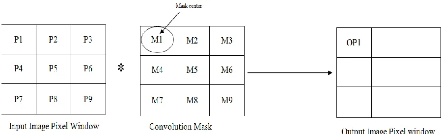
For instance, a two dimensional convolution using a 3×3 input image and 3×3 kernel would look
like as follows:
Figure 4.1: 2D Convolution Operation
16
4.2
Gaussian Mask
The Gaussian distribution in 1D has the following form:
𝑔 𝑥 =
1 2𝜋𝜎²𝑒
−𝑥²
2𝜎²
... (2)
In 2D, a circularly symmetric Gaussian has the form
𝑔 𝑥, 𝑦 =
2𝜋𝜎 ²1𝑒
−(𝑥2+𝑦 2)2𝜎 ²...
(3)
where
g
is the gaussian kernel weight at the location with coordinates
x
and
y
. The
σ
parameter is
the standard deviation of the Gaussian distribution which determines the sharpness or
smoothness of the Gaussian function. The term
2𝜋𝜎 ²1is normalization constant.
17
Figure 4.2: A 2D Gaussian Mask
The greatest advantage of the Gaussian filters of equation (3) is that they are separable. In
particular, the product of two 1D Gaussian functions gives a higher dimensional Gaussian
function and this can be represented mathematically as follows:-
𝑔 𝑥, 𝑦 = 𝑔 𝑥 𝑔(𝑦)
...
(4)
18
4.3
Steerable & Separable Gaussian Smoothing Filters
Directional or orientation filters are widely used in computer vision and image processing, such
as motion analysis, edge detection and texture analysis. In general, the shifts, edges and lines can
be characterized by a set of parameters including position, orientation, width or size. In order to
obtain the response of a filter at any arbitrary position and orientation it is very important to tune
the filters to all possible positions and orientations in real time. However, huge computations are
required in this way. The efficient way is to design a family of filters so that any filter in this
family can be represented by few basis filters. Therefore, the output of a filter can be expressed
as a weighted sum of basis filter outputs. Such filters are called “steerable filters”.
Steerability implies that the output
Oө
(
x
,
y
) of a filtering operation using a filter oriented at an
angle
𝜃
can be computed as the linear combination of a finite set of
M
outputs {
Oө
0(
x
,
y
),
Oө
1(
x
,
y
), ………..,
Oө
M-1(
x
,
y
) } obtained by applying the same filter oriented at directions
𝜃
0,
𝜃
1,…………,
𝜃
M-1, respectively. A 2D separable and steerable filter can be written as:
𝑔
θ𝑥, 𝑦 =
𝑅𝑟=−𝑅𝑔
iso𝑥 − 𝑟𝑐𝑜𝑠 𝜃 , 𝑦 − 𝑟𝑠𝑖𝑛 𝜃 𝑔
1D(𝑟)
... (5)
where it was assumed that the size of
𝑔
1D𝑟
is equal to
2R+1
.
The filter described in (5) can be applied to an image
I (x, y
) in two steps. In the first step, the
filter
𝑔
iso𝑥, 𝑦
is applied to the image.
19
In the second step, the following operation is applied to the image
𝐼
iso𝑥, 𝑦 .
𝐼
θ𝑥, 𝑦 =
𝑅𝑟=−𝑅𝐼
iso𝑥 − 𝑟𝑐𝑜𝑠 𝜃 , 𝑦 − 𝑟𝑠𝑖𝑛 𝜃 𝑔
1D𝑟
... (7)
The operation described in (6) and (7) is equivalent to the operation where the input image
I(x, y
)
is filtered by a Gaussian directional smoothing filter (DSF) oriented at direction
𝜃
. The function
𝑔
iso𝑥, 𝑦
describes a separable filter and can thus be implemented in an efficient manner. More
specifically,
𝑔
iso𝑥, 𝑦
can be expressed as
𝑔
iso𝑥, 𝑦 = 𝑔
x𝑥 𝑔
y(𝑦)
where
𝑔
x𝑥 =
2𝜋𝜎 21𝑥
𝑒
−𝑥2 2𝜎2
𝑥
and,
𝑔
y𝑦 = 𝑒
−𝑦2 2𝜎2𝑦.
Hence,
𝑔
iso𝑥, 𝑦
can be applied to
I (x, y
) by first filtering
I (x, y
) in a horizontal manner using
𝑔
x𝑥
and then by filtering the result in vertical manner using
𝑔
y𝑦
. Equation (7) describes a
linear combination of shifted versions of the image
𝐼
iso𝑥 − 𝑟𝑐𝑜𝑠 𝜃 , 𝑦 − 𝑟𝑠𝑖𝑛 𝜃
, which
depend on the filtering direction
𝜃
. The coefficients of the linear combination are equal to the
values of
𝑔
1D𝑟
. Image
𝐼
iso𝑥 − 𝑟𝑐𝑜𝑠 𝜃 , 𝑦 − 𝑟𝑠𝑖𝑛 𝜃
can be represented as the convolution
between the input image
I (x, y
) and the filter
𝑔
iso𝑥 − 𝑟𝑐𝑜𝑠 𝜃 , 𝑦 − 𝑟𝑠𝑖𝑛 𝜃
.
Thus, the proposed implementation is steerable in the sense that the final output
𝐼
θ𝑥, 𝑦
can be
expressed as a linear combination of the filtering operation outputs
𝐼
iso𝑥 − 𝑟𝑐𝑜𝑠 𝜃 , 𝑦 −
𝑟𝑠𝑖𝑛 𝜃
of a set of 2R+1 fundamental filters
𝑔
iso𝑥 − 𝑟𝑐𝑜𝑠 𝜃 , 𝑦 − 𝑟𝑠𝑖𝑛 𝜃
, parameterized by
20
The isotropic filter
𝑔
iso𝑥, 𝑦
is low pass and almost 100% of the energy of the filter is included
within the frequency band [
−3 𝜎
, 3 𝜎
x]
x. Therefore, the output
𝑔
iso𝑥, 𝑦
obtained by the
filtering the input image
I (x, y
) with
𝑔
iso𝑥, 𝑦
is band limited within the frequency range (-
𝜋, 𝜋
]
in any direction
𝜃
Thus, equation (7) can be modified without introducing significant aliasing.
𝐼
θ𝑥, 𝑦 =
[𝑅 𝐷𝑘=−[𝑅 𝐷 ] ]𝐼
iso𝑥 − 𝑘𝐷𝑐𝑜𝑠 𝜃 , 𝑦 − 𝑘𝐷𝑠𝑖𝑛 𝜃 𝑔
1D(𝑘𝐷)
... (8)
where
𝑔
1D(𝑟) = 𝑔 𝑘𝐷 =
12𝜋(𝜎𝑦2−𝜎𝑥2)
𝑒
−(𝑘𝐷 )²
2(𝜎 𝑦 2−𝜎 𝑥2)
... (9)
𝐷 =
𝜋𝜎3x,
is a down sampling factor ... (10)
[𝑅 𝐷
]
equals to the integer part of
[𝑅 𝐷
]
. Since the range of unique frequencies in discrete
signals is (-
𝜋, 𝜋
],
D
can be as large as the largest integer not greater that
𝜋𝜎
x3
, so that aliasing
21
CHAPTER 5
Hardware Implementation & Design Methodology
5.1
Hardware Implementation
This chapter explains in detail the reconfigurable hardware implementations of image processing
algorithms discussed in chapter 4, on a Xilinx VirtexII-Pro FPGA platform. The algorithms
implemented are:
General two dimensional convolution method
Separable convolution method 1 (using multiple BRAMs)
Separable convolution method 2 (using FIFO)
Steerable method
Convolution is one of the basic and common operations on images. It uses a sliding window
operator as discussed in section 4.2 of chapter 4. Based on the convolution operation, the
weighted sum of the input pixels within the window, considering that the window is centered at
pixel (
x
,
y
) is equal to the output at location (
x
,
y
). The weights are the values of the filter
assigned to every pixel of the window.
22
A single multiplication requires significant hardware resources and produces long delays. In
order to improve the performance of the convolution operation, it is necessary to reduce the
number of multiplications. Different techniques of performing multiplication on hardware are
explained in [20], [21]. Hence in the approach presented in this thesis, the algorithms are
developed by paying special attention to reducing the number of multiplications, thereby
decreasing the number of hardware resources while maintaining a satisfactory throughput in
terms of clock cycles.
5.2
Proposed Design Methodology
The main goal of this thesis is to implement steerable filtering techniques on FPGA efficiently.
The task is divided into steps which facilitate the building of the basic blocks. As described in
section 4.3 of chapter 4, the particular steerable filtering technique requires that the image is first
smoothed. This is achieved by convolving the original image with a Gaussian mask. This
convolution component is possibly the most important building block. Optimizing and pipelining
at this stage improves the implementation efficiency.
First, a small test image of 7×7 and a Gaussian mask of 3×3 were chosen for performing the
convolution operation. The two dimensional convolution operation was implemented using three
different approaches which are listed below:-
1)
General two dimensional convolution Method
23
A detailed explanation of each method, their performances and the associated logic utilization
along with algorithmic state diagrams are presented in the following subsections. For all methods
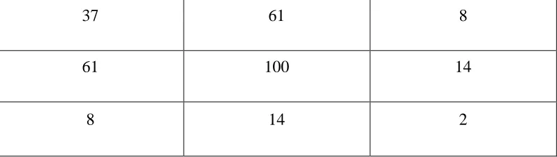
explained below, a test 7×7 image and a 3×3 Gaussian mask derived using equation (3) with
mean = 0 and standard deviation = 1and normalizing factor N = 0.0016 are considered. Each test
image pixel is represented using 16 bits and each mask value is also represented using 16 bits. A
7×7 test image and a 3×3 Gaussian mask are shown below:-
1
2
3
4
5
0
0
6
7
8
9
10
0
0
11
12
13
14
15
0
0
16
17
18
19
20
0
0
21
22
23
24
25
0
0
0
0
0
0
0
0
0
0
0
0
0
0
0
0
Table 5.1: A 7×7 Test Image
Table 5.2: A 3×3 Gaussian Mask with Mean = 0, σ = 1 and N = 0.0016
37
61
8
61
100
14
24
5.2.1 General two dimensional convolution method
In this method, BRAM is used to store a 7×7 test image using .coe file [31] which is generated
with Matlab. The Matlab program used for generating .coe file is available in the appendix. An
image controller is designed as a Finite State Machine (FSM) using VHDL to access the stored
image in the BRAM. VHDL code for image read/write controller is available in the appendix.
The obtained image pixels and mask pixels are controlled using pixel and mask controller
blocks. A multiplier is designed using the Intellectual Property (IP) core [32]. The inputs to the
multiplier are obtained from the pixel and mask controller blocks. The multiplier block generates
an output which is represented using 2
n
-1bits. The multiplier inputs are represented using
n
bits.
In this thesis work
n
was set equal to 16. The multiplier outputs are then given to an adder which
provides a 34 bit output. The adder output is the two dimensional convolution result between the
7×7 test image and the 3×3 Gaussian mask. The block diagram representation of two
dimensional convolution is shown below:-
25
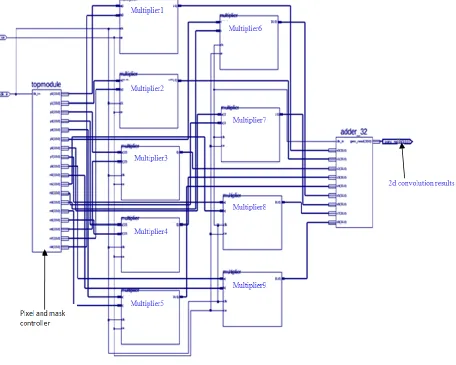
In the schematic diagram below, the block named as “topmodule” is the image and mask
controller. The module that stores the image in BRAM, and the image controller which reads the
image from BRAM are embedded in the topmodule block. The outputs of topmodule are
connected to 9 multipliers. The outputs of the 9 multipliers are finally connected to a 32 bit adder
named as “adder_32”. A 34 bit result obtained from adder_32 is the two dimensional
convolution between the 7×7 test image and the 3×3 Gaussian mask. A complete schematic
diagram of general two dimensional convolution method is shown below:-
26
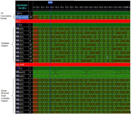
The schematic design is simulated using Xilinx ISIM simulator for verification purpose. In the
simulation diagram below, the reader may observe at the annotations, the image pixel controller
outputs and the mask controller outputs, the multiplier outputs, and finally, the two dimensional
convolution results. The simulation results are verified with Matlab and are provided in the
appendix. The simulation results of two dimensional convolution are shown below:-
27
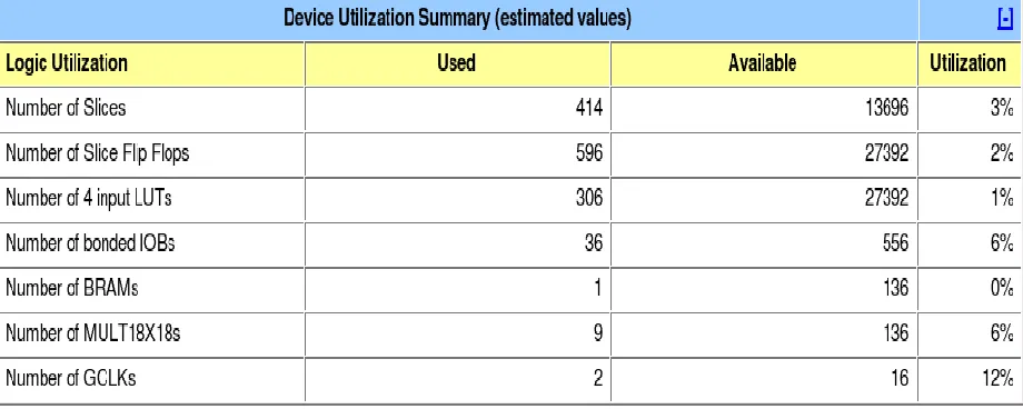
Finally, the overall design is simulated using Xilinx XST Synthesizer to obtain the logic or
hardware resource utilization on the target device. The design summary of the two dimensional
convolution method is shown below:-
Table 5.3: Device Utilization Summary of Two Dimensional Convolution Method
28
5.2.2 Separable convolution method 1(using multiple BRAMs)
As discussed in section 4.2 of chapter 4, a Gaussian mask is separable. The separable Gaussian
mask is derived using equations [3] and [4] with mean equal to zero, σ equal to zero and
normalizing factor N = 0.0016 are shown below:-
61
100
14
Table 5.4: Horizontal Gaussian Mask with Mean = 0, σ = 1 and N = 0.0016
61
100
14
Table 5.5: Vertical Gaussian Mask with Mean = 0, σ = 1 and N = 0.0016
29
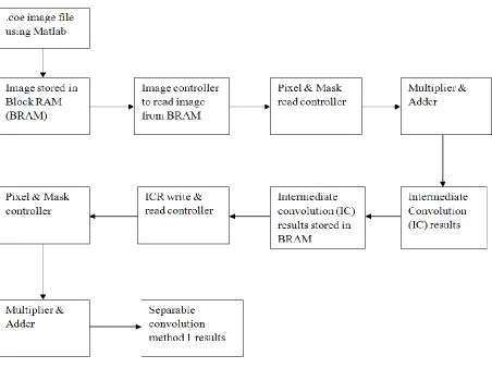
A write and read controller is designed as a FSM using VHDL for writing the vertical (or
intermediate) convolution result into the BRAM, and a read controller to read the intermediate
convolution results. At pixel and mask controller block, the vertical Gaussian mask pixels (34
bits) and the vertical convolution result pixels (34 bits) are accessed and given to multiplier and
adder block. The 70 bit output obtained is the final result of separable convolution using method
1 between the 7×7 test image and the 1×3 horizontal Gaussian mask. The block diagram
representation of separable convolution method 1 (using multiple BRAMs) is shown below:-
30
In the schematic diagram below, the block named “topmodule2” is the intermediate convolution
results write and read controller. The modules that store the image in BRAM and the image
controller which reads the image from BRAM are embedded in topmodule2 block. The outputs
of topmodule2 are connected to customfifo2. Customfifo2 access the required vertical
convolution results and horizontal mask pixels, which are then connected to the three multipliers.
The multiplier outputs are connected to an adder which provides a 70 bit output. The adder
output is the separable convolution between the 7×7 test image and the separable Gaussian
masks 3×1 & 1×3. A complete schematic diagram of separable convolution method 1 (using
multiple BRAMs) is shown below:-
31
The schematic design is simulated using Xilinx ISIM simulator for verification purpose. In the
simulation diagram below, the reader may observe at the annotations, the image pixel controller
outputs and mask controller outputs, the multiplier outputs and finally the separable convolution
method 1 results. The simulation results are compared with Matlab, and are provided in the
appendix. The simulation results of separable convolution method 1 are shown below:-
32
Finally, the overall design is simulated using Xilinx XST Synthesizer to obtain the logic or
hardware resource utilization on the target device. The design summary of the separable
convolution method 1 is shown below:-
Table 5.6: Device Utilization Summary of Separable Convolution Method 1
33
5.2.3 Separable convolution method 2 (using FIFO)
As discussed in section 4.2 of chapter 4, a Gaussian Mask is separable. Separable Gaussian mask
is derived using equations [3] and [4] with mean equal to zero, σ equal to 1 and normalizing
factor N = 0.0016 are shown below:-
61
100
14
Table 5.7: Horizontal Gaussian Mask with Mean = 0, σ = 1 and N = 0.0016
61
100
14
Table 5.8: Vertical Gaussian Mask with Mean = 0, σ = 1 and N = 0.0016
34
7 rows and 3 columns) in a 2D array vector. Parallelism is implemented, which yields in
obtaining final convolution result in parallel with the vertical or intermediate convolution result.
A read controller is designed to read the intermediate results saved in 2 dimensional arrays. At
pixel and mask controller block, vertical Gaussian mask pixels (34 bits) and vertical convolution
result pixels (34 bits) are accessed and given to multiplier and adder block. The 70 bit output
obtained is the final result of separable convolution using method 2 between the 7×7 test image
and the 1×3 horizontal Gaussian mask. The block diagram representation of separable
convolution method 2 (using FIFO) is shown below:-
35
In the schematic diagram below, the block named with “topmodule1” is the “intermediate
convolution results write and read controller”. The modules that store the image in BRAM and
the image controller which reads the image from BRAM are embedded in topmodule2 block.
The outputs of topmodule1 are connected to the separable2_controller. Separable2_controller
access required vertical convolution results and horizontal mask pixels which are then connected
to 3 multipliers. The multiplier outputs are connected to an adder which provides a 70 bit output.
The adder output is the separable convolution between the 7×7 test image and the separable
Gaussian masks 3×1 & 1×3. A complete schematic diagram of separable convolution method 2
(using FIFO) is shown below:-
36
The schematic design is simulated using Xilinx ISIM simulator for verification purpose. In the
simulation diagram below, the reader may observe at the annotations, the image pixel controller
outputs and mask controller outputs, the multiplier outputs and finally the separable convolution
method 2 results. The above obtained simulation results are verified with Matlab and are
provided in the appendix. The simulation results of separable convolution method 2 are shown
37
Finally, the overall design is simulated using Xilinx XST Synthesizer to obtain the logic or
hardware resource utilization on the target device. The design summary of separable convolution
method 2 is shown below:-
Table 5.9: Device Utilization Summary of Separable Convolution Method 2
38
5.2.4 Comparisons of convolution methods
For comparisons, we used a 7×7 test image and 3×3 Gaussian mask with both pixels represented
using 16 bits and the target device is XU2VP30-FFG896(-7). A comparison table is presented
below to explain which method is more feasible for applying steerability.
Table 5.10: Comparison of Convolution Methods
From the above comparisons, two dimensional convolution method is preferable as it uses few
resources with satisfactory performance. Practically, implementation might not be possible if we
go for larger mask sizes as it requires 3 clocks per pixel and more number of multipliers. Hence
the separable convolution method 2 is most favorable in terms of performance for larger mask
sizes, as it requires only 1 clock per pixel and less number of multipliers when compared with
two dimensional convolution.
Methods
(7×7 image and
3×3 Gaussian
mask)
Slices
[13696]
Slice flip
flops
[27392]
4 input
LUT’s
[27392]
Bonded
IOBs
[556]
BRA
Ms
[136]
Multipli
ers
[136]
Clock
s per
pixel
Two
Dimensional
convolution
414 (2%) 596(2%)
306(1%)
36(6%)
1(0%)
9(6%)
~3
Separable
Convolution
Method 1
579(4%)
553(2%)
729(2%)
72(12%) 2(1%)
15(11%) ~2
Separable
Convolution
Method 2
39
5.2.5 Extension of separable convolution method 2 (using FIFO)
The chosen convolution method i.e. separable convolution method 2 (using FIFO) is extended
for a larger image of 48×48 and a separable Gaussian masks of 1×9 and 9×1. A Matlab program
was used for generating 48×48 gray scale image is provided in the appendix. Image pixels are
represented using 8 bits. Separable Gaussian masks of 1×9 and 9×1 derived using equation [3] &
[4] with mean equal to zero, σ equal to 1 and normalizing factor N = 0.0016 are shown below:-
Table 5.11: Horizontal Gaussian Mask with Mean = 0, σ = 1 and N = 0.0016
Table 5.12: Vertical Gaussian Mask with Mean = 0, σ = 1 and N = 0.0016
100
61
14
1
0
0
0
0
0
40
A complete schematic diagram of separable convolution method 2 extended to a larger image of
48×48 and separable Gaussian masks of 9×1 and 1×9 is shown below:-
41
The schematic design is simulated using Xilinx ISIM simulator for verification. In the simulation
diagram below, the reader may observe at the annotations, the image pixel controller outputs and
mask controller outputs, the multiplier outputs and finally the separable convolution method 2
results. The above obtained simulation results are verified with Matlab. The simulation results of
separable convolution method 2 extended to a larger image of 48×48 and separable Gaussian
masks of 9×1 and 1×9 is shown below:-
42
The design summary of separable convolution method 2 extended to a 48×48 image size and
Gaussian mask of 9×1 and 1×9 are shown below:-
Table 5.13: Device Utilization Summary of Separable Convolution Method 2 extended to 48×48
image size and Gaussian mask of 9×1 and 1×9
In the simulation results, it can be observed that the total number of clock cycles required for
completing the separable convolution between a 48×48 test image and a 9×1 & 1×9 Gaussian
masks using the method of FIFO is equal to 2130. Hence the separable convolution method 2
(using FIFO) is approximately 1 clock per pixel.
43
6.3
Proposed Steerable Concept Implementation
Steerability is applied on the obtained results of separable convolution (method 2) between the
48×48 image and the Gaussian masks of 9×1 and 1×9. For applying steerability, a steerable
Gaussian mask is derived using equation (9) and decimation factor using the equation (10).
The derived steerable Gaussian masks of 7×1 and 1×7 for mean = 0, σx = 3, σy = 5, Normalizing
factor N = 0.001and decimation factor D = 3 are shown below:-
8
33
76
100
76
33
8
Table 5.14: Horizontal Gaussian Mask with Mean = 0, σ
x= 3, σ
y= 5, N = 0.001
8
33
76
100
76
33
8
44
In the steerable concept, we access pixels in different directions depending on the decimation
factor. Then, the pixels are multiplied with the weights of Gaussian mask and finally given to
adder to obtain final steerable results in a particular direction. For example, the decimation factor
used here is
D
= 3. The pixels are accessed in different directions such as horizontal, vertical,
diagonal and etc which are at a distance of 3 from each other and this is continued till the end of
the image. The final results obtained in each particular direction are our required steerable
results. The block diagram representation of implementing steerable concept on the results of
separable convolution method 2 in horizontal and vertical direction is shown below:-
45
A complete schematic diagram of steerable implementation on 48×48 image using Gaussian
mask of 7×1 and 1×7 in horizontal, vertical and diagonal directions is shown below:-
Figure 5.13: Schematic Diagram of Steerable Implementation
46
The design summary of steerable implementation on 48×48 image using Gaussian mask of 7×1
and 1×7 in horizontal, vertical and diagonal directions is obtained for a Xilinx Virtex4 shown
below:-
Table 5.16: Device Utilization summary of steerable implementation on a virtex4 board.
47
CHAPTER 6
Conclusions & Future Work
6.1
Summary & Conclusions
The following summary and conclusions were drawn based on implementation and
experimentation:-
1.
Three different techniques of convolution are developed and an assessment of these
methods is prepared by considering device resource utilization and performance in
terms of clocks per pixel.
2.
The second separable implementation presented in this thesis requires the smallest
number of clock cycles per pixels compared to the other implementations.
3.
The concept of steerability is applied in horizontal, vertical and diagonal directions on
a 48×48 smoothed image. The smoothed image is obtained by convolving the original
image 48×48 with 1×9 & 9×1 Gaussian masks. Three 7×1 Gaussian masks were used
for the steerable outputs, which are acquired by convolving original using Gaussian
mask of 7×1. The steerable filtering technique is synthesized and its effectiveness is
confirmed using simulation results.
48
6.2
Limitations
The following limitations are listed below:-
1.
The target device VirtexII Pro is not supported for implementation by newer versions
of Xilinx ISE Design Suite Software (11 and higher versions).
2.
The previous version i.e. ISE 10.3 has software bugs which does not provide proper
simulation and synthesis results when a large number of multipliers are used.
6.3
Future Work
The following work has to be performed in order to improve the efficiency of hardware
implementation of steerability concept.
1.
An efficient way of accessing image pixels along different directions from block RAM in
less number of clock cycles.
2.
Exploring an efficient way of representing image and mask pixels in less number of bits.
3.
Efficient methods of dropping off the unused most significant bits before and after the
multiplier or adder stage thereby reducing resource utilization of multipliers.
49
Bibliography
1.
Moore’s Law made real by Intel Innovations www.intel.com/technology/mooreslaw/
2.
Dr. Dimitrios Charalampidis, “ Efficient Directional Gaussian Smoothers”, IEEE
Geoscience and Remote Sensing, July 2009
3.
D. Brown, R. Francis, J. Rose, Z. Vransic, Field-Programmable Gate Arrays, Kluwer
Academic Publishers, May 1992.
4.
Pong P. Chu, A text book on “FPGA prototyping by VHDL examples Xilinx Spartan 3
version”. 2008
5.
J. Webster, A document on “Programmable Logic Arrays”, Wiley Encyclopedia of
Electrical and Electronics Engineering, 1999
6.
Richard Waln, Ian Bush, Martyn Guest, Miles Deegan, Igor Kozln and Christine Kitchen,
A report on “An overview of FPGAs and FPGA programming; Initial experiences at
Daresbuy”, Nov 2006.
7.
Xilinx, “ ISE 10.3 Design Suite and software manuals”,
http://www.xilinx.com/itp/xilinx10/books/manuals.pdf
8.
Xilinx , “Xilinx University Program Virtex-II Pro Development System Hardware
Reference Manual-UG069”, July 2009
50
10.
Daggu Venkateshwar Rao and Muthukumar Venkatesan , “Implementation and
Evaluation of Image Processing Algorithms on Reconfigurable Architecture using
C-based Hardware Descriptive Languages”, International Journal of Engineering and
Applied Sciences, 2006
11.
IEEE Std 1076, “ IEEE Standard VHDL Language Reference Manual”, Jan 2000
12.
V. Lakshmanan, “A Separable Filter for Directional Smoothing”, IEEE Geoscience and
Remote Sensing Letters, July 2004.
13.
William T. Freeman and Edward H. Adelson, “The Design and Use of Steerable Filters”,
IEEE Transaction of Pattern Analysis and Machine Intelligence, Sept 1991.
14.
C. Chou, S. Mohana krishnan, J. Evans, “FPGA Implementation of Digital Filters”, Proc.
ICSPAT, 1993
15.
Hui Zhang, Mingxin Xia, and Guangshu Hu, “A Multiwindow Partial Buffering Scheme
for FPGA Based 2-D Convolvers, IEEE Transaction on Circuits and Systems, Feb 2007.
16.
Dr. Haled Benkrid, Mr. Samir Belkacemi, “Design and Implementation of a 2D
Convolution Core for Video Applications on FPGAs”, International Workshop on Digital
and Computational Video, Nov 2002.
17.
Franscisco Cardells-Tormo, Pep-Lluis Molinet,” Area Efficient 2-D Shift Variant
Convolvers for FPGA Based Digital Image Processing”, IEEE Transaction on Circuits
and Systems, Feb 2006.
51
19.
Bruce A. Draper, J. Ross Beveridge, A.p Willem Bhom, Charles Ross, Monica
Chawathe, Jeffrey Hammes, A publication on “Accelerated Image Processing on
FPGAs”, 2008.
20.
G. Sutter, E. Todorovich, G.Bioul, M. Vazquez, J-P. Deschamps, “FPGA Implementation
of BCD Multipliers”, International Conference on Reconfigurable Computing and
FPGAs, 2009.
21.
Lakshmanan, Masuri Othman and Mohamad Alauddin Mohd. Ali, “High Performance
Parallel Multiplier using Wallace-Booth Algorithm”, Proceeding of ICSE, 2002.
22.
Schoeters Jurgen, Van Winkel Jan, Goedeme Toon, Meel Jan, “In-Vehcile Movie
Streaming using an Embedded System with MOST Interface”, Automative
Electronics-3
rdInstitution of Engineering and Technology Conference, June 2007.
23.
A. W. Azman, A. Bigdeli, Y. M. Mustafah, B. C. Lovell, “ Optimizing Resources of an
FPGA-based Smart Camera Architecture”, Proceedings of Digital Image Computing
Techniques and Applications, 2008.
24.
WM EI-Medany, MR Hussain,” FPGA Based Advanced Real Traffic Light Controller
System Design”, IEEE International Workshop on Intelligent Data Acquisition and
Advanced Computing Systems: Technology and Applications, Sept 2007.
25.
Justin L. Tripp, Henning S. MOrtveit, Anders A. Hanson, Maya Gokhale, “ Metropolitan
Road Traffic Simulation on FPGAs”, IEEE symposium on Field-Programmable Custom
Computing Machines, 2005.
52
27.
Peter Mc. Curry, Fearghal Morgan, Liam Kilmartin,” Xilinx Implementation of Pixel
Processor for Object Detection Applications”, Proceedings of Signals and Systems
Conference, 2001.
28.
Paul D. Fiore, Dane Kottke, Wojciech Krawiec, David Campagna, “ Efficient Feature
Tracking with Application to Camera Motion Estimation”, IEEE , 2002
29.
Kah-Howe Tan, Wen Fung Leong, Sameer Kadam, M.A Soderstrand and Louis G.
Johnson, “ Public Domain Matlab Program to Generate Highly Optimized VHDL for
FPGA Implementation”, IEEE, 2001.
30.
K. R. Castleman, M. Schulze, Q, Wu, “Simplified Design of Steerable Pyramid Filters”,
IEEE Proceedings, 1998.
53
Appendix
2D Convolution Method VHDL Source Files
---
-- filename: dualportram_image_controller.vhd
-- author: Arjun Joginipelly
---
library IEEE;
use IEEE.STD_LOGIC_1164.ALL; use IEEE.STD_LOGIC_ARITH.ALL; use IEEE.STD_LOGIC_UNSIGNED.ALL;
---- Uncomment the following library declaration if instantiating ---- any Xilinx primitives in this code.
--library UNISIM;
--use UNISIM.VComponents.all;
entity dualportram_image_controller is Port ( clk_in : in STD_LOGIC;
douta : in STD_LOGIC_VECTOR (15 downto 0); addra : out STD_LOGIC_VECTOR (5 downto 0); dina : out STD_LOGIC_VECTOR (15 downto 0); wea : out STD_LOGIC;
ena : out STD_LOGIC;
p0 : out std_logic_vector (15 downto 0); p1 : out std_logic_vector (15 downto 0); p2 : out std_logic_vector (15 downto 0); p3 : out std_logic_vector (15 downto 0); p4 : out std_logic_vector (15 downto 0); p5 : out std_logic_vector (15 downto 0); p6 : out std_logic_vector (15 downto 0); p7 : out std_logic_vector (15 downto 0); p8 : out std_logic_vector (15 downto 0);
m0 : out std_logic_vector (15 downto 0); m1 : out std_logic_vector (15 downto 0); m2 : out std_logic_vector (15 downto 0); m3 : out std_logic_vector (15 downto 0); m4 : out std_logic_vector (15 downto 0); m5 : out std_logic_vector (15 downto 0); m6 : out std_logic_vector (15 downto 0); m7 : out std_logic_vector (15 downto 0); m8 : out std_logic_vector (15 downto 0); clk_out : out STD_LOGIC);
end dualportram_image_controller;
54
type state_reg_type is (initialstate,state1,state2,state3,state4, state5,state6,state7,state8,state9,halt);
signal sreg:state_reg_type:=initialstate;
signal acount:std_logic_vector(5 downto 0):="000000"; signal addra_sig:std_logic_vector(5 downto 0):="000000"; signal data_present:std_logic:='0';
signal p0_sig:std_logic_vector(15 downto 0):=(others=>'0'); signal p1_sig:std_logic_vector(15 downto 0):=(others=>'0'); signal p2_sig:std_logic_vector(15 downto 0):=(others=>'0'); signal p3_sig:std_logic_vector(15 downto 0):=(others=>'0'); signal p4_sig:std_logic_vector(15 downto 0):=(others=>'0'); signal p5_sig:std_logic_vector(15 downto 0):=(others=>'0'); signal p6_sig:std_logic_vector(15 downto 0):=(others=>'0'); signal p7_sig:std_logic_vector(15 downto 0):=(others=>'0'); signal p8_sig:std_logic_vector(15 downto 0):=(others=>'0');
begin
clk_out<=clk_in; process(clk_in) begin
if(clk_in'event and clk_in<='0') then case sreg is
when initialstate=> wea<='0';
ena<='1';
sreg<=state1;
when state1=> data_present<='0'; p0_sig<=douta;
addra_sig<=addra_sig+1; sreg<=state2;
when state2=> p1_sig<=douta;
addra_sig<=addra_sig+1; sreg<=state3;
when state3=> p2_sig<=douta;
addra_sig<=addra_sig+5;
sreg<=state4;
when state4=> p3_sig<=douta;
addra_sig<=addra_sig+1; sreg<=state5;
when state5=> p4_sig<=douta;
addra_sig<=addra_sig+1; sreg<=state6;
when state6=> p5_sig<=douta;
addra_sig<=addra_sig+5; sreg<=state7;
55
addra_sig<=addra_sig+1; acount<=acount+1; sreg<=state8;
when state8=> p7_sig<=douta;
addra_sig<=addra_sig+1; sreg<=state9;
when state9=> p8_sig<=douta; addra_sig<=acount; data_present<='1'; if(acount=50) then sreg<=halt; else sreg<=state1; end if; when halt=> wea<='0';
ena<='0'; end case; end if; end process; process(data_present) begin
56
---
-- filename: multiplier.vhd
-- author: Arjun Joginipelly
---
LIBRARY ieee;
USE ieee.std_logic_1164.ALL; -- synthesis translate_off Library XilinxCoreLib; -- synthesis translate_on ENTITY multiplier IS
port (
clk: IN std_logic;
a: IN std_logic_VECTOR(15 downto 0); b: IN std_logic_VECTOR(15 downto 0); ce: IN std_logic;
p: OUT std_logic_VECTOR(31 downto 0)); END multiplier;
ARCHITECTURE multiplier_a OF multiplier IS -- synthesis translate_off
component wrapped_multiplier port (
clk: IN std_logic;
a: IN std_logic_VECTOR(15 downto 0); b: IN std_logic_VECTOR(15 downto 0); ce: IN std_logic;
p: OUT std_logic_VECTOR(31 downto 0)); end component;
-- Configuration specification
for all : wrapped_multiplier use entity XilinxCoreLib.mult_gen_v10_1(behavioral) generic map(
c_a_width => 16, c_b_type => 1,
c_ce_overrides_sclr => 0, c_has_sclr => 0,
c_round_pt => 0, c_model_type => 0, c_out_high => 31, c_verbosity => 0, c_mult_type => 1, c_ccm_imp => 0, c_latency => 1, c_has_ce => 1,
c_has_zero_detect => 0, c_round_output => 0, c_optimize_goal => 1,
c_xdevicefamily => "virtex2p", c_a_type => 1,
c_out_low => 0, c_b_width => 16,
57
-- synthesis translate_on BEGIN
-- synthesis translate_off U0 : wrapped_multiplier
port map (
clk => clk, a => a, b => b, ce => ce, p => p); -- synthesis translate_on
END multiplier_a;
---
-- filename: adder.vhd
-- author: Arjun Joginipelly
---
library IEEE;
use IEEE.STD_LOGIC_1164.ALL; use IEEE.STD_LOGIC_ARITH.ALL; use IEEE.STD_LOGIC_UNSIGNED.ALL;
---- Uncomment the following library declaration if instantiating ---- any Xilinx primitives in this code.
--library UNISIM;
--use UNISIM.VComponents.all;
entity adder_32 is
Port ( clk_in : in STD_LOGIC;
x0 : in STD_LOGIC_VECTOR (31 downto 0); x1 : in STD_LOGIC_VECTOR (31 downto 0); x2 : in STD_LOGIC_VECTOR (31 downto 0); x3 : in STD_LOGIC_VECTOR (31 downto 0); x4 : in STD_LOGIC_VECTOR (31 downto 0); x5 : in STD_LOGIC_VECTOR (31 downto 0); x6 : in STD_LOGIC_VECTOR (31 downto 0); x7 : in STD_LOGIC_VECTOR (31 downto 0); x8 : in STD_LOGIC_VECTOR (31 downto 0);
genc_result : out STD_LOGIC_VECTOR (33 downto 0)); end adder_32;
architecture Behavioral of adder_32 is
58
signal x8_sig:std_logic_vector(33 downto 0);
begin
process(clk_in,x0,x1,x2,x3,x4,x5,x6,x7,x8) begin
x0_sig<="00" & x0; x1_sig<="00" & x1; x2_sig<="00" & x2; x3_sig<="00" & x3; x4_sig<="00" & x4; x5_sig<="00" & x5; x6_sig<="00" & x6; x7_sig<="00" & x7; x8_sig<="00" & x8;
genc_result<=x0_sig+x1_sig+x2_sig+x3_sig+x4_sig+x5_sig+x6_sig+x7_sig +x8_sig;
end process;
end Behavioral;
---
-- filename: resultmodule.vhd
-- author: Arjun Joginipelly
--- library ieee; use ieee.std_logic_1164.ALL; use ieee.numeric_std.ALL; library UNISIM; use UNISIM.Vcomponents.ALL;
entity resultmodule is
port ( ce : in std_logic; clk_in : in std_logic;
genc_result : out std_logic_vector (33 downto 0)); end resultmodule;
59
signal XLXN_19 : std_logic_vector (15 downto 0); signal XLXN_20 : std_logic_vector (15 downto 0); signal XLXN_21 : std_logic_vector (15 downto 0); signal XLXN_22 : std_logic_vector (15 downto 0); signal XLXN_23 : std_logic_vector (15 downto 0); signal XLXN_39 : std_logic_vector (31 downto 0); signal XLXN_40 : std_logic_vector (31 downto 0); signal XLXN_41 : std_logic_vector (31 downto 0); signal XLXN_42 : std_logic_vector (31 downto 0); signal XLXN_43 : std_logic_vector (31 downto 0); signal XLXN_44 : std_logic_vector (31 downto 0); signal XLXN_45 : std_logic_vector (31 downto 0); signal XLXN_46 : std_logic_vector (31 downto 0); signal XLXN_47 : std_logic_vector (31 downto 0);
attribute box_type:string; component topmodule
port ( clk_in : in std_logic;
p0 : out std_logic_vector (15 downto 0); p1 : out std_logic_vector (15 downto 0); p2 : out std_logic_vector (15 downto 0); p3 : out std_logic_vector (15 downto 0); p4 : out std_logic_vector (15 downto 0); p5 : out std_logic_vector (15 downto 0); p6 : out std_logic_vector (15 downto 0); p7 : out std_logic_vector (15 downto 0); p8 : out std_logic_vector (15 downto 0); m0 : out std_logic_vector (15 downto 0); m1 : out std_logic_vector (15 downto 0); m2 : out std_logic_vector (15 downto 0); m3 : out std_logic_vector (15 downto 0); m4 : out std_logic_vector (15 downto 0); m5 : out std_logic_vector (15 downto 0); m6 : out std_logic_vector (15 downto 0); m7 : out std_logic_vector (15 downto 0); m8 : out std_logic_vector (15 downto 0)); end component;
component multiplier
port ( a : in std_logic_vector (15 downto 0); b : in std_logic_vector (15 downto 0); clk : in std_logic;
ce : in std_logic;
p : out std_logic_vector (31 downto 0)); end component;
component adder_32
port ( clk_in : in std_logic;
![Figure 2.1: Architecture of a generic FPGA [3]](https://thumb-us.123doks.com/thumbv2/123dok_us/8945947.1855315/14.612.85.494.296.664/figure-architecture-of-generic-fpga.webp)
![Figure 2.2: Architecture of Logic Block with one 4-input LUT [3]](https://thumb-us.123doks.com/thumbv2/123dok_us/8945947.1855315/15.612.69.508.354.591/figure-architecture-logic-block-input-lut.webp)
![Figure 2.4: Picture of XUP VirtexII Pro Board [8]](https://thumb-us.123doks.com/thumbv2/123dok_us/8945947.1855315/18.612.75.530.107.639/figure-picture-of-xup-virtexii-pro-board.webp)