Dynamic Power Reduction in NOC by Encoding
Techniques
Shivaraj MN Ravi H Talawar
PG Student Assistant Professor
Department of Digital Electronics and Communication System Department of Digital Electronics and Communication System VIAT, VTU, CPGS, Bengaluru Region, Muddenahalli,
Chikkaballapur, Karnataka, India
VIAT, VTU, CPGS, Bengaluru Region, Muddenahalli, Chikkaballapur, Karnataka, India
Abstract
As technology improve the size will be reduced, and the power dissipated by the links of a network-on-chip (NoC) is starts to participate with the power dissipate by the other element of communication system, for example the routers and the network interfaces (NIs). We design an set of data encoding technique by different schemes to decrease the power dissipation by an links of NoC, which optimizing the on-chip communication system not only in terms of performance but also in terms of power. The idea presented in this paper is base on encoding the packets before they are inserted in to the network in such a way as to minimize both the switching action and the coupling-switching action in the NoC‟s link which represent the main factor of power dissipation. These schemes were universal and transparent with respect to the construct NoC fabric that means this application will not require any change in the router and link of architecture. These will be carried in both artificial and real traffic scenario. These effective of the proposed scheme will tolerate to save the energy consumption and power dissipation without changing the performance degradation and with less area consumption in the NI.
Keywords: switching action, encoding, network-on-chip (NoC), low power, router, Network interfaces (NIs)
_______________________________________________________________________________________________________
I.
I
NTRODUCTIONMoving towards silicon technology node to the next results faster and more efficient gates but slower because there is a more power hungry wires. More than 50% of total dynamic power is dissipate in interconnection in current processor, and this was expected to increase more over in the next several years. Global interconnect length does not scale with smaller transistors and local wires. Chip size remains relatively constant because the chip function continues for instance the RC delay increases exponentially. The RC delay in a 1-mm worldwide wire at the smallest pitch is superior to the intrinsic delay of a two-input NAND fan-out. If the raw computation horsepower seems to be un-limited, thanks to the ability of instance more core‟s in a single silicon chip, scalable issue occur, due to making an efficient and reliable communication among the increasing number of core‟s, become the real problem. The NOC invent is documented as the most feasible way to tackle with scalable and variability issue that characterize the ultra-deep sub-micron-meter.
Now a days in the on-chip communication issue is relevant, in some of the case more relevant than commutating related issue. The communication sub-system more and more impacts the usual designed objective, and also includes cost (i.e., area of silicon), performances, dissipation of power, consumption of energy and reliability. As technology improves the size is reducing and more fraction of total power is budget of the complex in more core of the system-on-chip (SoC) this is because of communication sub-system.
Here we attentation on the technique aim to minimize power dissipation by a network link. The power dissipation in the network is relevant as that dissipation by NIs, routers and it is giving that ordinary to increase the technology scale. We are representing the set of encoding schemes for data which is in binary formate, and it is operated at flit level, and an end-to-end basis, this allows us to minimize the switching action and coupling switching action at the link of an direction is traverse by a packet. This encoding schemes, were transparent by respect to router execution, and they are presented, discussed in both algorithmic-level and architectural level, it is assessed via the simulation in the artificial, real traffic scenario. These analysis gives an different aspects, metrics design, it include area of silicon, energy consumption and dissipation of power. From the results we can conclude that with these proposed encoding schemes that power will save and also energy will be save without changing any major degradation in the performance in the NIs.
II.
M
OTIVATION AND RELATED WORKtechnique, its mainly focus is to reduce the link power. The encoding technique‟s is categorize in to two group. In 1st group we are going to decrease the power by the self-switching action of the each bus line and avoid the dissipation of power by coupling switching action.
These work concentrate on the different component of the inter connection network such as NIs, router, and link. Because these will reduce power dissipation by an link, in this paper, we are going to brief the review some works in the region of link power reduction. These include the technique that make use of shielding, which increase line-to-line space and repeater inserted. They all increases the silicon chip area. These encode scheme is an additional technique that is employed to reduce dissipation of power in link. The data encoding technique has been classified in to two class. In the first class, encoding technique concentrate on reducing the power due to self-switching action of separate bus line while ignoring an power dissipation due to their coupling-switching action. In these class, bus invert (BI) and INC-XOR have been proposed for these case that casual random data pattern is transmitte through the lines. On the other hand, gray code, T0, working-zone encoding, and T0-XOR were suggest for the case of correlation data pattern. Application particular approach have also been proposed
This class of encoding will not be appropriate to be applied in the deep sub-micron meter technological node where the coupling capacitance constitute an most important part of the total inter-connect capacitance. This will cause the power consumption due to the coupling-switching action to become a big fraction of the total power consumption in the links, that making the aforementioned techniques, which ignore such contributions, inefficient. The works in the second class concentrate on reducing power dissipation through the reducing the coupling-switching action. Among these schemes, the switching action is reduced by using many additional control lines. For example, the data bus width grows from 32 to 55. The techniques proposed in have a smaller number of control lines but the complexity of their decoding logic is high. The technique described as follows: first, the data are both odd inverted and even inverted, and afterwards transmission is perform using these kind of inversion which reduce more switching action. The coupling switching action it is reduced, this is compared with another, so we use a simple decoder although achieving a higher activity reduction.
The scheme presented is to reduce the coupling switching action. In this method, encoder count the number of Type I (Table I) transitions with a weighting coefficient of one and the number of Type II transitions with the weighting coefficient of two. If the number is larger than half of the link width, the inversion will be performed. In addition to the complex encoder, the method only works on the patterns whose full inversion leads to the link power reduction while not considering the patterns whose full inversions may lead to high link power consumption. So the link power reduction achieved through this technique is not as large as it could be. This scheme was also based on the hop-by-hop technique.
In another coding technique presented in, bunches of four bits are encoded with five bits. The encoded bits were isolated using shielding wires such that the occurrence of the patterns “101” and “010” were prevented. This way, no simultaneous Type II transitions in two adjacent pair bits are induced. This technique effectively reduces the coupling switching activity. Although the technique reduces the power consumption considerably, it increases the data transfer time, and, hence, the link energy consumption. This is due to the fact that for each four bits, six bits are transmitted which increases the communication traffic. This technique was also based on the hop-by-hop approach.
III.
O
VERVIEW OF THE PROPOSALThe fundamental idea of the proposed technique is, the packet are transferred via the network after that the bits are encoded. This technique will help to decrease the switching action and coupling switching action in the link of network traversed by the packets. This self-switching and coupling switching movement are responsible for the link power dissipation. Here we are going to refer to end-to-end scheme. Based on the end to end scheme we are having a improved advantage. The advantage is a pipeline nature of the switching technique. Since same sequence of all the packets passes through all the links of the routing path. T he NI may provide the same power saving for all the links. The advanced scheme, an encoder and decoder block are added to the NI. The encoder encode all the going bits of the packets at the other side the header bit such that the power dissipate by the inner router and point to point link is decrease.
IV.
P
ROPOSED ENCODING SCHEMESThe main goal of this encoding scheme is to reduce the power dissipation by decreasing the coupling transition performance on the link of the inter connection network. In this they are classified 4 types of coupling transitions. A type-I occur when one of the line is switch and remaining one is unchanged. A type-II occurs when one of the lines switches from low to high and another is switch from high to low. A type-III occur both the line switches at the same time. A type-IV occurs when both the lines are remains unchanged. The coupling switching action (Tc) is defined as a weight sum of different type of coupling transition contribution There-fore
TC=K1T1+K2T2+K3T3+K4T4
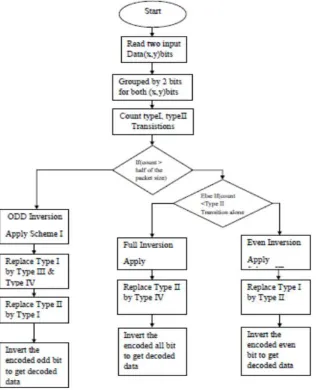
Fig. 1: Flow chart of Proposed Encoding technique
Scheme I A.
In scheme 1, our main goal is to decrease the number of Type-I transition and Type-II transition. Type-I transition is convert into Type III and Type IV transition and Type II transition is converted into Type I transition. This scheme compare the two data„s based on to reducing the link power reduction by doing odd inversion or no inversion operation with the help of Table-1
Table 1: Effect of Even inversion on change of Transition Types
(a)
(b)
Fig. 1: Scheme-I (a) Block diagram. (b) Architecture of encoder block
Ty > Tx eq... (2) Ty > 0.5 (w-1) eq... (3)
number of type-1 transition and type-2 transition is happening means it set the output state to „1‟, or else it set the output to „0‟. The odd inversion is performed for these type of transitions. Then the next block is the Majority code it checks the state, if the number of 1‟s is greater than 0‟s or not and it implement using a simple circuit. The final stage using the XOR circuit, these circuit is used to perform the inversion on odd- bits. The decoding is perform by just invert the encoder circuit when the inverting bit is high.
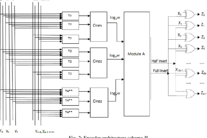
Fig. 2: Encoder architecture scheme-II
Scheme II B.
In the scheme-II encoding, we are going to implement the odd and the full inversion. In these inversion procedure is to convert the Type-II to Type-IV transitions. In these scheme it compare the present data with earlier one it will choose whether we want to do Odd, Full or No inversion to present data which will give power reduction in link.
T2 > T4** ... (4)
Fig. 4: Decoder architecture scheme-II
The block diagram of the decoder is shown in Fig.3. The w-1 bits input is applied in the decoder circuit and another input of the decoder is previous decoded output. The decoder block compare the two input data„s and invert operation is performed and w-1 bits output is produced. The remaining one bit is used to indicate the inversion is performed or not. Then the decoder output is given to the gray to binary block. This block converts the gray code into original binary input. In decoder circuit diagra m (Fig.4.) consist of TY block and Majority vector and XOR circuits. Based on the encoder action the TY block is determined the transitions. Based on the transitions types the majority blocks checks the validity of the inequality given by (2). The output of the majority is given to the XOR circuit. Half inversion, full inversion and no inversion is performed based on the logic gates.
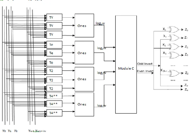
Scheme III C.
In scheme III, we are adding the even inversion into scheme II. Because the odd inversion converts Type-I transitions into Type II transitions. From table II, T1 **/T1*** are converted into Type IV/Type III transitions by the flits is even inverted. The link power reduction in even inversion is larger than the Odd inversion.
V.
R
ESULTS AND DISCUSSIONFig.6. shows the simulation result of schem- I (reducing Type I and Type II transitions) using this encoding technique. The output of the scheme I reducing the number of Type-I and Type-II transitions by using the odd invert condition. Fig.7. shows the simulation result of scheme-II (convert Type II transitions into Type-IV ) using these encoding techniques. Fig.7. shows the simulation result of scheme-III the number of type II transition is converted into Type IV transitions by using the odd and full inversion condition.
(a)
(b)
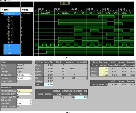
Fig. 6: shows the simulation result of schem- I (a) Output waveform and (b) Power details of SchemeI I
(b)
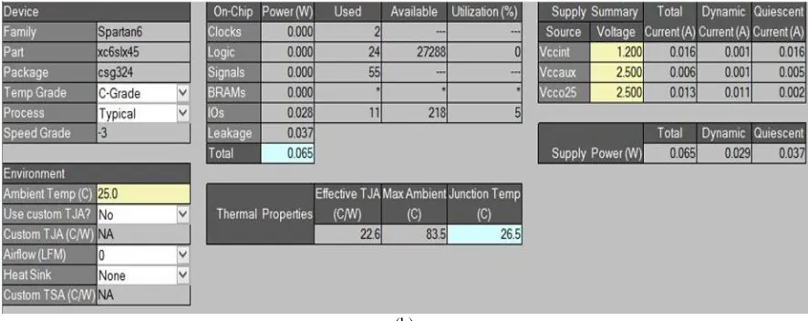
Fig. 7: shows the simulation result of schem-II (a) Output waveform and (b) Power details of Scheme-II
(a)
(b)
Fig. 8: shows the simulation result of schem-III (a) Out put waveform and (b) Power details of Scheme-III
VI.
C
ONCLUSIONby using a cycle and bit exact NoC simulator under both artificial and real traffic scenario. The application of an proposed encoded scheme which allow saving of energy consumption and power dissipation without any major performance degradation and with less consumption in the NI.
R
EFERENCES[1] Nima Jafarzadeh, Maurizio Palesi, Ahmad , and Afzali-Kusha, ―Data Encoding Techniques for Reducing Energy Consumption in Network-on-Chip‖ IEEE
Trans. Very Large ScaleIntegr. (VLSI) Syst,Mar.2014.
[2] International Technology Roadmap for Semiconductors. (2011) [Online].Available: http://www.itrs.net
[3] D. Yeh, L. S. Peh, S. Borkar, J. Darringer, A. Agarwal, andW. M. Hwu, ―Thousand-core chips roundtable,‖ IEEE Design Test Comput., vol. 25, no. 3, pp.
272–278, May–Jun. 2008.
[4] D. Yeh, L. S. Peh, S. Borkar, J. Darringer, A. Agarwal, andW. M. Hwu, ―Thousand-core chips roundtable,‖ IEEE Design Test Comput., vol. 25, no. 3, pp.
272–278, May–Jun. 2008.
[5] M. Ghoneima, Y. I. Ismail, M. M. Khellah, J. W. Tschanz, and V. De, ―Formal derivation of optimal active shielding for low-power on-chip buses,‖ IEEE
Trans. Comput.-Aided Design Integr. Circuits Syst., vol. 25, no. 5, pp. 821–836, May 2006.
[6] L. Macchiarulo, E. Macii, and M. Poncino, ―Wire placement for crosstalk energy minimization in address buses,‖ in Proc. Design Autom.Test Eur. Conf.
Exhibit. Mar. 2002, pp. 158–162.
[7] R. Ayoub and A. Orailoglu, ―A unified transformational approach for reductions in fault vulnerability, power, and crosstalk noise and delay on processor
buses,‖ in Proc. Design Autom. Conf. Asia South Pacific, vol. 2. Jan. 2005, pp. 729–734.
[8] K. Banerjee and A. Mehrotra, ―A power-optimal repeater insertion methodology for global interconnects in nanometer designs,‖ IEEETrans. Electron
Devices, vol 49, no. 11, pp. 2001–2007, Nov. 2002.
[9] M. R. Stan and W. P. Burleson, ―Bus-invert coding for low-power I/O,‖ IEEE Trans. Very Large Scale Integr. (VLSI) Syst., vol. 3, no. 1, pp. 49–58, Mar.
1995.
[10] S. Ramprasad, N. R. Shanbhag, and I. N. Hajj, ―A coding framework for low-power address and data busses,‖ IEEE Trans. Very Large ScaleIntegr. (VLSI) Syst. vol. 7, no. 2, pp. 212–221, Jun. 1999.
[11] C. L. Su, C. Y. Tsui, and A. M. Despain, ―Saving power in the control path of embedded processors,‖ IEEE Design Test Comput., vol. 11, no. 4, pp. 24–
31, Oct.–Dec. 1994.
[12] L. Benini, G. De Micheli, E. Macii, D. Sciuto, and C. Silvano, ―Asymptotic zero-transition activity encoding for address busses in low-power
microprocessor-based systems,‖ in Proc. 7th Great Lakes Symp. VLSI, Mar. 1997, pp. 77–82.
[13] E. Musoll, T. Lang, and J. Cortadella, ―Working-zone encoding for reducing the energy in microprocessor address buses,‖ IEEE Trans. VeryLarge Scale
Integr.(VLSI) Syst., vol. 6, no. 4, pp. 568–572, Dec. 1998.
[14] S. Youngsoo, C. Soo-Ik, and C. Kiyoung, ―Partial bus-invert coding for power optimization of application-specific systems,‖ IEEE Trans. VeryLarge Scale Integr.(VLSI) Syst., vol. 9, no. 2, pp. 377–383, Apr. 2001.
[15] Z. Yan, J. Lach, K. Skadron, and M. R. Stan, ―Odd/even bus invert with two-phase transfer for buses with ,‖ in Proc. Int. Symp. LowPower Electron.
Design, 2002, pp. 80–83.
[16] Z. Yan, J. Lach, K. Skadron, and M. R. Stan, ―Odd/even bus invert with two-phase transfer for buses with ,‖ in Proc. Int. Symp. LowPower Electron.
Design, 2002, pp. 80–83.
[17] K. W. Ki, B. Kwang Hyun, N. Shanbhag, C. L. Liu, and K. M.Sung, ―Coupling-driven signal encoding scheme for low-power interface design,‖ in Proc.
IEEE/ACM Int. Conf. Comput.-Aided Design, Nov. 2000, pp. 318–321.
[18] M. Palesi, G. Ascia, F. Fazzino, and V. Catania, ―Data encoding schemes in networks on chip,‖ IEEE Trans. Comput.-Aided Design Integr. CircuitsSyst.,
vol. 30 no. 5, pp. 774–786, May 2011.
[19] M. Palesi, G. Ascia, F. Fazzino, and V. Catania, ―Data encoding schemes in networks on chip,‖ IEEE Trans. Comput.-Aided Design Integr. CircuitsSyst.,