Volume -3, Issue - 4, July - August 2017, Page No. 12 - 19
Pag
e
12
Development of Cascade Full- Bridge Dual Buck Inverter with Phase-Shift Control Various PWM Techniques
Hafsa Fathima1, Dr.Jaghannath.K2, D.Kumara Swamy3
1
M. Tech scholar, Dept of EEE, SVS Institute of Technology, Hanamkonda, T.S, India
2
Assistant Professor, Dept of EEE, SVS Institute of Technology, Hanamkonda, T.S, India
3
Associate Professor, HOD, Dept of EEE, SVS Institute of Technology, Hanamkonda, T.S, India
Abstract
Cascade H-bridge inverter has been widely used in various applications, especially where separate DC sources naturally
exist in the places, such as Photovoltaics, fuel cells, battery energy storage, and electric vehicle drives. The advantages of
cascade type inverters include the capability of reaching higher output voltage level by using standard lower voltage
devices, and the modular design concept which makes the maintenance less burdensome.. The proposed cascade dual
buck inverter with phase-shift control inherits all the merits of dual buck type inverters and overcomes some of their
drawbacks. Compare to traditional cascade inverters, it has much enhanced system reliability thanks to no shoot-through
problems and lower switching loss with the help of using power MOSFETs. With phase-shift control, it theoretically
eliminates the inherent current zero-crossing distortion of the single-unit dual buck type inverter. In addition, phase-shift
control and cascade topology can greatly reduce the ripple current or cut down the size of passive components by
increasing the equivalent switching frequency. A cascade dual buck inverter has been designed and tested to demonstrate
the feasibility and advantages of the system by comparing single-unit dual buck inverter, 2-unit and 3-unit cascade dual
buck inverters at the same 1 kW, 120 V ac output conditions. Hybrid PWM technique leads to better performance of the
cascade dual-buck full-bridge inverter as compared to cascade H bridge, it provides less output current ripple and
harmonics, no zero-crossing distortion, and higher efficiency
Keywords: MOSFET, Frequency, Meter, Voltage, Power, CASCADE.
1. Introduction
Numerous industrial applications have begun to require higher power apparatus in recent years. Some medium voltage
motor drives and utility applications require medium voltage and megawatt power level. For a medium voltage grid, it is
troublesome to connect only one power semiconductor switch directly. As a result, a multilevel power converter
structure has been introduced as an alternative in high power and medium voltage situations. A multilevel converter not
only achieves high power ratings, but also enables the use of renewable energy sources. Renewable energy sources such
as photovoltaic, wind, and fuel cells can be easily interfaced to a multilevel converter system for a high power
application.
The concept of multilevel converters has been introduced since 1975. The term multilevel began with the three-level
converter. Subsequently, several multilevel converter topologies have been developed. However, the elementary concept
of a multilevel converter to achieve higher power is to use a series of power semiconductor switches with several lower
voltage dc sources to perform the power conversion by synthesizing a staircase voltage waveform. Capacitors, batteries,
13
13
13
13
13
13
13
13
13
13
13
13
13
13
13
13
13
13
13
13
13
switches aggregate these multiple dc sources in order to achieve high voltage at the output; however, the rated voltage of
the power semiconductor switches depends only upon the rating of the dc voltage sources to which they are connected.
Advantages and Disadvantages
A multilevel converter has several advantages over a conventional two-level converter that uses high switching
frequency pulse width modulation (PWM). The attractive features of a multilevel converter can be briefly summarized as
follows.
Staircase waveform quality: Multilevel converters not only can generate the output voltages with very low
distortion, but also can reduce the dv/dt stresses; therefore electromagnetic compatibility (EMC) problems can be
reduced.
Common-mode (CM) voltage: Multilevel converters produce smaller CM voltage; therefore, the stress in the
bearings of a motor connected to a multilevel motor drive can be reduced. Furthermore, CM voltage can be
eliminated by using advanced modulation strategies
Input current: Multilevel converters can draw input current with low distortion.
Switching frequency: Multilevel converters can operate at both fundamental switching frequency and high
switching frequency PWM. It should be noted that lower switching frequency usually means lower switching loss
and higher efficiency.
Unfortunately, multilevel converters do have some disadvantages. One particular disadvantage is the greater number of
power semiconductor switches needed. Although lower voltage rated switches can be utilized in a multilevel converter,
each switch requires a related gate drive circuit. This may cause the overall system to be more expensive and complex.
Plentiful multilevel converter topologies have been proposed during the last two decades Contemporary research has
engaged novel converter topologies and unique modulation schemes. Moreover, three different major multilevel converter
structures have been reported in the literature: cascaded H-bridges converter with separate dc sources, diode clamped
(neutral- clamped), and flying capacitors (capacitor clamped). Moreover, abundant modulation techniques and control
paradigms have been developed for multilevel converters such as sinusoidal pulse width modulation (SPWM), selective
harmonic elimination (SHE-PWM), space vector modulation (SVM), and others. In addition, many multilevel converter
applications focus on industrial medium-voltage motor drives, utility interface for renewable energy systems, flexible AC
transmission system (FACTS), and traction drive systems.
2. Topology and Operation Principle
The single-unit dual buck inverter has two basic forms, dual buck half-bridge inverter [22], [24] and dual buck full-bridge
Pag e
14
Pag e14
Pag e14
Pag e14
Pag e14
Pag e14
Pag e14
Pag e14
Pag e14
Pag e14
Pag e14
Pag e14
Pag e14
Pag e14
Pag e14
Pag e14
Pag e14
Pag e14
Pag e14
Pag e14
Pag e14
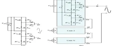
Figure 1: Topology of cascade dual buck half-bridge inverter.
Two types accordingly: cascade dual buck half-bridge inverter, shown in Fig. 1, and cascade dual buck full-bridge
inverter, shown in Fig. 3. This paper will focus on the analysis, design, and testing of the cascade dual buck half-bridge
inverter to demonstrate the feasibility and advantages of cascade dual buck inverters. In [24], the control strategy for two
dual buck half-bridge inverters in series output to obtain higher voltage was proposed. However, the two dual buck
inverters shared the same dc power supply, had two sets of filter inductor and capacitor, and the connection was only
effective for two units. The proposed inverter in this paper features a different series connection concept, the cascading,
which has separate dc power supplies for each cell, and is extended to N unit connection, and shares the same filter
components. Fig. 1 shows the topology of the proposed cascade dual buck half-bridge inverter. It consists of N units of
single dual buck half-bridge inverter. Each unit is composed of two power MOSFETs and two fast recovery diodes. Each
unit has two output ports, iP and iN (i = 1, 2. . . N). To realize the cascade topology, the iN port of the ith unit is connected
with the (i +1)P port of the (i + 1)th unit, and port 1P and NN are used as the output ports.Sip and Dip are a working pair,
and operate at the positive half-cycle of output current i. Sin and Din are another working pair, and operate at the negative
half-cycle of output current i. The single unit operation modes are shown in Fig. 2 [22],
Figure 2 : Operation modes of single-unit dual buck half-bridge inverter.(a) Positive current, S1p turned ON. (b) Positive
15
15
15
15
15
15
15
15
15
15
15
15
15
15
15
15
15
15
15
15
15
3. Phase-Shift Control Analysis
One of the significant characteristics of a single-unit dual buck type inverter is that the switch is selectively working based
on the direction of output current. From the operation modes of single-unit half-bridge dual buck inverter in Fig. 2, we can
clearly see that when i1 is positive, S1p andD1p are the working pair, and when i1 is negative, S1n and D1n are the
working pair. However, this distinctive operation leads to its inherent drawback, current zero-crossing distortion, which
will be explained in detail below. This issue can be passively mitigated by turning on both S1p and S1n near zero-crossing
period.
Figure 3: Single-unit dual buck full-bridge inverter serving as one cell for cascade dual buck full-bridge inverter.
(a) Single-unit dual buck full-bridge inverter.(b) Cascade dual buck full-bridge inverter.
Figure 4: Equivalent circuit of single-unit half-bridge dual buck inverter when S1p is ON.
However, this remedy is against the operating principle and the best feature of the dual buck type inverter, which is high
reliability by avoiding turning on both active switches at the same time. In addition, this passive measure results in higher
switching losses because at zero-crossing period two switches are switching while the original goal of dual buck inverter
is to have only one switch operating at any given time.
Pag
e
16
Pag
e
16
Pag
e
16
Pag
e
16
Pag
e
16
Pag
e
16
Pag
e
16
Pag
e
16
Pag
e
16
Pag
e
16
Pag
e
16
Pag
e
16
Pag
e
16
Pag
e
16
Pag
e
16
Pag
e
16
Pag
e
16
Pag
e
16
Pag
e
16
Pag
e
16
Pag
e
16
4. Simulation Diagram And Result
The analysis, design and implementation of the cascade dual-buck inverters has been carried out and presented in this
chapter. Compared to traditional cascade inverters, cascade dual-buck inverters have enhanced system reliability, no dead
time and shoot-through concerns and they can achieve lower switching losses with the help of using power MOSFETs.
Simulation result of dual-buck full-bridge inverter under AHCU PWM
Figure 7: Simulation diagram of Single dual-buck inverter
Figure 8: Simulation diagram of Bipolar PWM and Uni-Polar PWM
The output of sliding mode controller is the actual speed which is estimated from motor current and voltage as its input.
The controller is designed with the help of above equations which is described in section VI.
17
17
17
17
17
17
17
17
17
17
17
17
17
17
17
17
17
17
17
17
17
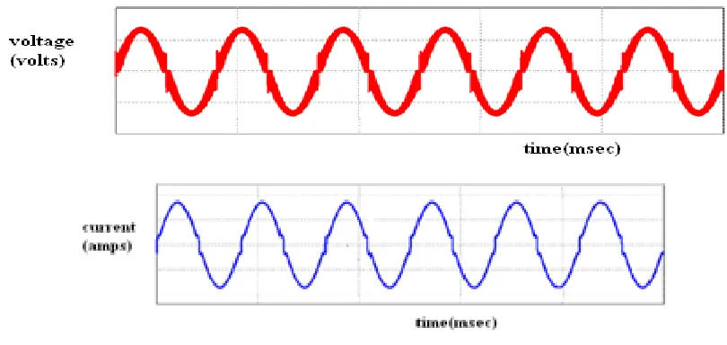
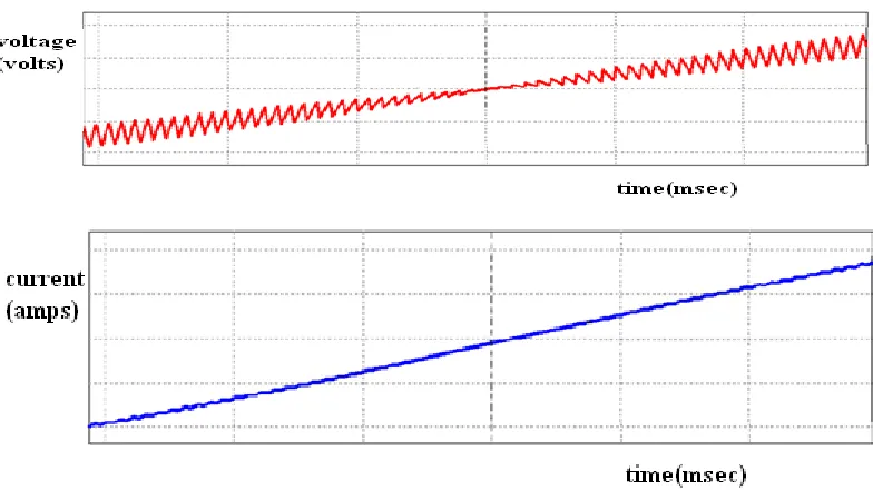
Figure 10: Waveforms of voltage and current at zero crossing
(a) Waveforms of voltage and current
Pag e
18
Pag e18
Pag e18
Pag e18
Pag e18
Pag e18
Pag e18
Pag e18
Pag e18
Pag e18
Pag e18
Pag e18
Pag e18
Pag e18
Pag e18
Pag e18
Pag e18
Pag e18
Pag e18
Pag e18
Pag e18
5. References[1]. Arash A. Boora, Alireza Nami, Firuz Zare, Arindam Ghosh, and Frede Blaabjerg,( Oct 2010 ) “Voltage-Sharing
Converter to Supply Single Phase Asymmetrical Four-Level Diode Clamped Inverter With High Power Factor Loads”,
IEEE Trans On Power Electronics, Vol. 25, No. 10, Pp. 2507-2520.
[2]. Baoming Ge, Fang Zheng Peng, Aníbal T. de Almeida, and Haitham Abu-Rub, (Aug 2010) “An Effective Control
Technique for MediumVoltage High-Power Induction Motor Fed by Cascaded Neutral-Point-Clamped Inverter”, IEEE
Trans On Industrial Electronics, Vol. 57, No. 8, pp. 2659-2668.
[3]. C. Attaianese, M. Di Monaco, and G. Tomasso, (2010) “Three-Phase Three-Level Active NPC Converters for High
Power System”, International Symposium on Power Electronics, Electrical Drives, Automation and Motion, pp. 204-209,
Speedam.
[4]. Grain P. Adam, Stephen J. Finney, Ahmed M. Massoud, and Barry W. Williams, ( Aug 2008) “Capacitor Balance
Issues of the Diode-Clamped Multilevel Inverter Operated in a Quasi TwoState Mode” IEEE Trans On Industrial
Electronics, Vol. 55, NO. 8, pp. 3088- 3099 .
[5]. H. K. Al-Hadidi, A. M. Gole, and David A. Jacobson, (April 2008) “A Novel ConFigureuration for a Cascade
Inverter-Based Dynamic Voltage Restorer With Reduced Energy Storage Requirements”, IEEE Trans. On Power
Delivery, Vol. 23, No. 2, pp. 881-888.
[6]. J. Liu, and Y. Yan, (2003) “A Novel Hysteresis Current Controlled Dual Buck Half Bridge Inverter”, in Proc. IEEE
PESC, 2003, pp. 1615-1620.
[7]. Jeffrey Ewanchuk, John Salmon, and Behzad Vafakhah, (Sept/Oct 2011) “A Five-/Nine-Level
TwelveSwitchNeutral-Point-Clamped Inverter for High-Speed Electric Drives”, IEEE Trans on Industry Applications, Vol. 47, No. 5, pp.
2145-2153.
[8]. Jin Li, Jinjun Liu, Dushan Boroyevich, Paolo Mattavelli, and Yaosuo Xue, (Dec 2011) “Three-level Active
Neutral-Point-Clamped Zero-CurrentTransition Converter for Sustainable Energy Systems”, IEEE Trans. On Power Electronics,
Vol. 26, No. 12, pp. 3680-3693.
[9]. Jin Li, Jinjun Liu, Dushan Boroyevich, Paolo Mattavelli, and Yaosuo Xue, (May 30-June 3, 2011) “Comparative
Analysis of Three-Level Diode Neural-PointClamped and Active Neural-Point-Clamped Zero-Current-Transition
Inverters”, 8th International Conference on Power Electronics, pp. 2290-2295.
[10]. Jun Li, Subhashish Bhattacharya, and Alex Q. Huang, (March 2011) “A New Nine-Level Active NPC (ANPC)
Converter for Grid Connection of Large Wind Turbines for Distributed Generation”, IEEE Trans On Power Electronics,
Vol. 26, No. 3, pp. 961-972.
[11]. Marcelo C. Cavalcanti, Alexandre M. Farias, Kleber C. Oliveira, Francisco A. S. Neves, and João L. Afonso, (Jan
2012) “Eliminating Leakage Currents in Neutral Point Clamped Inverters for PhotovoltaicSystems”, IEEE Trans. On
19
19
19
19
19
19
19
19
19
19
19
19
19
19
19
19
19
19
19
19
19
[12]. Pablo Lezana, José Rodríguez, and Diego A. Oyarzún, (March 2008)“Cascaded Multilevel Inverter With
Regeneration Capability and Reduced Number of Switches”, IEEE Trans. On Industrial Electronics, Vol. 55, No. 3, pp.
1059-1066.
[13]. Robert Stala, (Sept 2011) “Application of Balancing Circuit for DC-Link Voltages Balance in a Single-Phase
Diode-Clamped Inverter With Two Three-Level Legs”, IEEE Trans On Industrial Electronics, Vol. 58, No. 9, pp. 4185-4195.
[14]. Z. Yao, L. Xiao, and Y. Yan, (Aug 2009)“Dual-Buck Full-Bridge Inverter With Hysteresis Current Control”, IEEE
Trans. Ind. Electron., vol. 56, no. 8, pp. 3153–3160.
[15]. Zhiguo Pan, Fang Zheng Peng, Keith A.Corzine, Victor R. Stefanovic, John M. (Mickey) Leuthen, and Slobodan
Gataric, (Nov/Dec 2005) “Voltage Balancing Control of DiodeClamped Multilevel Rectifier/Inverter Systems” IEEE