Iranian Journal of Electrical & Electronic Engineering, Vol. 14, No. 1, March 2018 1
Implementation of Low-Cost Architecture for Control an
Active Front End Rectifier
A. Hamidi*, A. Ahmadi*,** and S. Karimi*(C.A.)
Abstract: In AC-DC power conversion, active front end rectifiers offer several advantages over diode rectifiers such as bidirectional power flow capability, sinusoidal input currents and controllable power factor. A digital finite control set model predictive controller based on fixed-point computations of an active front end rectifier with unity displacement of input voltage and current to improve dynamic response has been presented in this paper. Here by using a predictive cost function and fixed-point computations, the optimal switching state to be applied in the next sampling is selected. The low-cost architecture is implemented on a FPGA platform. Designed architecture is constructed based on fixed-point arithmetic with minimal functional units. The control algorithm, which is used in this architecture, is Finite-Set Model Predictive Control (FS-MPC). Compared with other controllers, this controller provides a much better dynamic performance. Finally, in order to evaluate the accuracy of the fixed-point computations several cases for various loading conditions and word lengths are verified.
Keywords: Active Front End Rectifier, Fixed-Point Computations, Low-Cost Architecture, Predictive Control, Word Length.
1 Introduction1
CTIVE-FRONT-END Rectifiers (AFE) are currently a well-suited alternative to diode rectifiers, because they produce sinusoidal input currents with unity displacement power factor, low harmonic input current and bidirectional power flow [1], [2]. AFE rectifier can be used in renewable energies and active power filter where interconnection stages are essential [3]. Different control scheme applied to power electronic converters have been classified as; Voltage Oriented Control (VOC) and Direct Power Control (DPC) which is investigated in [4]. Recently, finite-control-set model-predictive-control has been successfully addressed to control AFEs [5]. It has been successfully applied to several power electronics
Iranian Journal of Electrical & Electronic Engineering, 2018. Paper first received 10 July 2017 and accepted 16 December 2017. * The authors are with the Electrical Engineering Department, Razi University, Kermanshah, Iran.
E-mails: [email protected] and [email protected]. ** The author is with the Department of Electrical and Computer Engineering, University of Windsor, Windsor, ON, Canada.
E-mail: [email protected]. Corresponding Author: S. Karimi.
devices as such as DC-DC converters (buck and boost), DC-AC converters (Two-level VSI, Neutral Point Clamped, Cascaded H-Bridge Inverter and Flying-Capacitor Inverter), AC-DC converters (Single- phase Boost Converter, Asymmetric Half Bridge converter, Active-Front-End Rectifier and Current Source Rectifier) and AC-AC converters (Modular Multilevel Converter, Direct Matrix Converter and Indirect Matrix Converter) [6]. Model Predictive Control (MPC) offers many advantages; in particular, it can be used in a variety of process, being simple to apply in multivariable systems. Furthermore, the inclusion of nonlinearities and constraints in the control law is straightforward [6]. Moreover, this scheme does not require internal current control loops and modulators, which greatly reduces its complexity. This digital control technique has successfully been applied to a wide range of power converters, drives and energy system applications [7], [8]. In Finite Control Set Model Predictive (FCS-MPC) there are limited number of switching states of the power converter for solving the optimization problem and a cost function is used as a criterion to select the optimal future actions [9], [10]. This control technique uses a model of the system to calculate predictions of the future behavior of the
A
Iranian Journal of Electrical & Electronic Engineering, Vol. 14, No. 1, March 2018 2 system for a given set of possible actuations for a
predefined time horizon. The sequence of actuations that minimizes a cost function, which synthesizes the control objectives, is selected, and the first element of the sequence is applied. This optimization is repeated every sampling time considering the new measured data [11]. In this work, a FCS-MPC technique has been used to control an AFE rectifier with unity power factor. FCS-MPC uses a discrete-time model of the system and selects the optimal firing actuation to converter for the next sampling period based on minimum cost function [12].
In the present study, the basic purpose is to evaluate a low-cost architecture of a digital controller for an AC-DC rectifier using FCS-MPC concept. As a proof of concept, the controller is implemented on a FPGA platform (Xilinx vertex II), based on predictive control and fixed point arithmetic. In previous works, controllers are implemented using based block-diagram high level synthesis tools, such as XILINX VIVADO or ALTERA QUARTUS. These synthesis tools provide an easy design platform using functional description of the algorithm, but design details are hidden from designer, which makes it suitable for lab prototyping of the design, but it is not applicable for industrial designs in which designer needs an optimized implementation suitable for embedded or integrated circuit hardware realization. For instance, accuracy and implementation cost (bit-width vs. required hardware) is normally ignored in automated design synthesis. Further, without deep knowledge of hardware design and synthesis, proper trade-offs between different design parameters such as, implementation cost, speed, reliability, precision and power consumption are not possible. In this work, unlike previous works, we present an explicit design architecture and details, which give the transparency to future designers to acquire this design approach and apply modifications for further improvements and/or industrial applications.
With this approach, the controller design is optimum in terms of required resources (only two adder and two multiplier), which makes it an efficient candidate for an integrated circuit implementation of this controller. With this approach variety of switching control algorithms can be transformed to firmware hardware with practical industrial application. There are several challenges in transforming a software algorithm to a firmware design including: required resources, limitation of mathematical operations in hardware, precision, data management and control.
In this work computation accuracy is evaluated for different word-lengths. There is a trade-off between word-length and hardware cost. This scheme predicts behavior of future input currents for each switching state of the converter. The cost function evaluates predicted value for input currents with their references and minimizes the error between them at the end of each sampling time and then the optimum switching states
apply to power switches.
The paper is organized as follows. In Section 2, the Operation of the AFE rectifier is analyzed. In Section 3, the model predictive control of active front end rectifier is introduced. In Section 4, hardware implementation is presented. In Section 5, implementation results are presented and the conclusions are presented in Section 6.
2 Operation of the AFE Rectifier
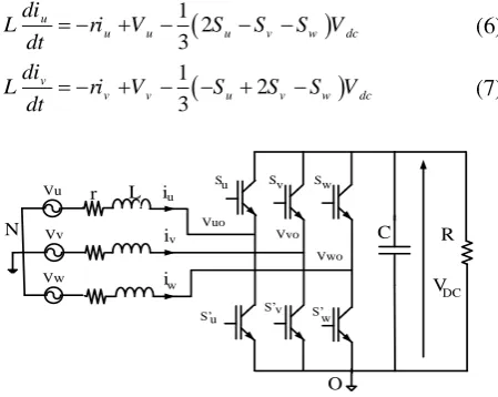
The AFE rectifier topology is shown in Fig. 1 which corresponds to a fully controlled three phase bridge with semiconductor switches(IGBTs) connected to the three-phase voltage supply (Vu, Vv, Vw) using the input filter inductances (L) and resistances (r). The model of the ac side of the rectifier is:
0 0
u
u u u N
di
V ri L V V
dt
0 0
v
v v v N
di
V ri L V V
dt
0 0
w
w w w N
di
V ri L V V
dt
0N
V is the common mode voltage between the floating neutral of the source and the negative bus of the rectifier, considering balanced input voltages and no neutral current, can be calculated as [13]:
0 0 0
0
3
u v w
N
V V V
V
Considering each rectifier voltage given by
0 , 0 , 0
u u dc v v dc w w dc
V S V V S V V S V
where Su, Sv, Sw are the switching states (1 if the corresponding upper switch is ON or 0 if it is OFF) and
Vdc is the dc voltage. According to the above equations the ac side can be modeled as:
1 2 3 u
u u u v w dc
di
L ri V S S S V
dt
1
2 3
v
v v u v w dc
di
L ri V S S S V
dt
Lf u S u S’u Sv S’v Sw S’ w C R r L Vu Vv Vw N VDC i u
i i v
w
O Vuo
Vvo Vwo
Fig. 1 AFE rectifier topology.
Iranian Journal of Electrical & Electronic Engineering, Vol. 14, No. 1, March 2018 3
1
2 3
w
w w u v w dc
di
L ri V S S S V
dt
The dc side of the converter is modeled as
dc dc
u u v v w w
dV V
c i S i S i S
dt R
where R is the load resistance and C is the dc-link capacitance.
Re-writing the model using vector variables, the model of the AC side becomes
s
s s s dc
di
L ri v MS V
dt
where , ,
u u u
s v s v s v
w w w
V i S
V V i i S S
V i S
and
2 1 1
1 2 1
1 1 2
1 3
M
.
The DC side can be expressed as
T dc dc
s s
dV V
C i S
dt R
3 Model Predictive Control of Active Front End Rectifier
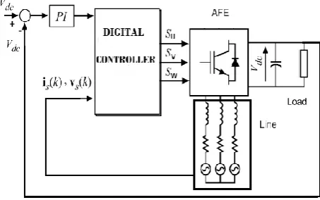
Model Predictive Control (MPC) has now approximately three decades of sustained development and offers many advantages; MPC is a control scheme based on the search of the optimal input to achieve a desired output. As in power electronics the inputs belong to a finite set, this control strategy is well suited for power converters [14]. The MPC techniques applied to Power Electronics have been classified into two main categories [7], [8]: Continuous Control Set MPC and Finite Control Set MPC (FCS-MPC). In the first group, a modulator generates the switching states starting from the continuous output of the predictive controller. On the other hand, the FCS-MPC approach takes advantage of the limited number of switching states of the power converter for solving the optimization problem. A discrete model is used to predict the behavior of the system for every admissible actuation sequence up to the prediction horizon. The switching action that minimizes a predefined cost function is finally selected to be applied in the next sampling instant. The main advantage of FCS-MPC lies in the direct application of the control action to the converter, without requiring a modulation stage [11]. A simplified control block diagram for control of an AFE rectifier is shown in Fig. 2. In this block diagram the input currents (is(k)) and input voltages (vs(k)) measured and apply to digital
controller. Output voltage (Vdc) measured and compared with its reference (Vdc*), then apply to PI controller. PI controller is used to set reference currents (Iref) from the error signal between the measured and reference DC voltage. The predictive controller uses a current reference which obtained by the dc-link PI controller, the output of the dc-voltage controller is multiplied by the input voltage in order to obtain the in phase sinusoidal references.
In digital controller the future current (ip[k+1]) will predict then compared with its reference (i*[k+1]) by
cost function. The cost function minimizes the error between the predicted currents and their references at the end of each sampling time. Finally, the switching state that minimize the cost function apply to IGBTs. To find a suitable discrete model of the converter a first order forward difference approximation of the derivative can be used [13]. In the AFE rectifier the current derivatives are calculated as
1
, , ,
sp s
s
s
i k i k
di
s u v w
dt T
where Ts is sampling time. According to these equations, the discrete model of the AFE rectifier is given by
1
s
sp s L s s dc
T
i k i k K V k MS V k
L
where KL=1-rTs/L. The currents error of each input can
be defined as
*
1 1
s s sp
e i k i k
where is* is current reference. The cost function is calculated by
T s s
g e e
4 Hardware Implementation
FPGAs contain an array of programmable logic blocks, and a hierarchy of reconfigurable interconnects
Fig. 2 Proposed control scheme for the rectifier.
Iranian Journal of Electrical & Electronic Engineering, Vol. 14, No. 1, March 2018 4 that allow the blocks to be wired together, like many
logic gates that can be inter-wired in different configurations. Some of the major disadvantages of the conventional microprocessor or DSP controls could overcome by using FPGA, because it can be designed to perform any application and is not specific to a particular function. The FPGA can be more efficient than the conventional controller due to fast prototyping, software design and simple hardware design. Also, the written code is almost independent from the architecture of the device and the hardware is reconfigured easily. Other advantages over other traditional devices are different and probably shorter design cycles, low-power consumption, and higher density for implementing digital control system [15].
The FPGA is suitable for systems which require relatively simple computation and fast processing time; complex control algorithms with complicated computations could be easier implemented by software in the FPGA, as they may embed a true microprocessor. The results of this co-design is increasing the flexibility of the designed system and reducing the development time [16]. The speed, size, and the number of I/O pins of a modern FPGA far exceed that of a microprocessor or DSP. These features allow to improve the implementation of predictive control algorithm by means of calculates the next step currents and error functions for all the inputs simultaneously [13].
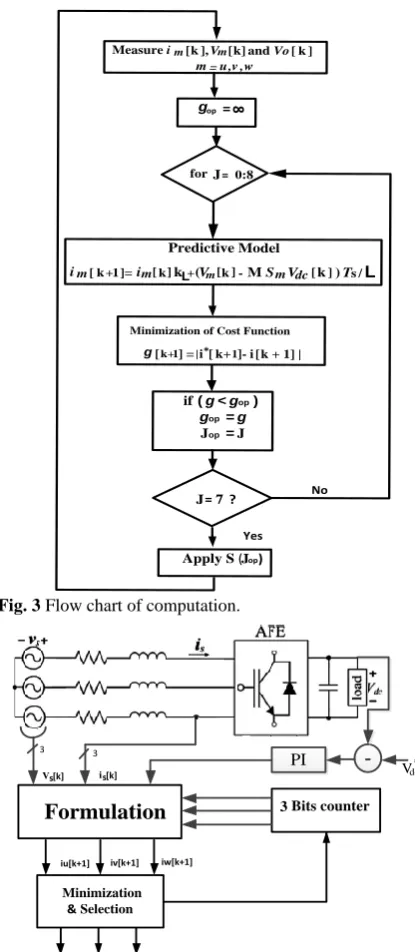
The biggest issue in the most of previous approaches, however, is their hardware design approach. Since hardware implementation of the control algorithm is a multidisciplinary field, it is a challenge for power electronic designers to consider and solve both control algorithm issues and hardware design efficiency at the same time. Our approach presents a new direction in this regard. We are introducing a design method based on a predefined soft-architecture in which hardware datapath is synthesized. This approach provides a solution for power electronic engineers by which they can design efficient control hardware with minimum cost. This is different from a microcontroller-based approach which is limited to the hardware resources available on the microcontroller chip. Also, it is different from other FPGA-based approaches and automatic synthesis tools, which either offer simplified drag and synthesis methods by hiding design complexity or offer a large amount of hardware and FPGA parameters and professional design details. In this section, we present and analyze the implementation details of the fixed-point based architecture. Our purpose is to control the current in fixed-point based architecture for different word-lengths. For simulation results, component designs were coded in VHDL. Our target device is Xilinx vertex II, which contains 4.3 Mb on-chip memory and Xilinx ISE development tools were used to simulate and synthesize our architecture. The controller has implemented on FPGA and control signals have achieved. The flow
chart of computation is shown in Fig. 3. In this flow chart since we have three switches (Su, Sv, Sw) thus 8 (23) switching states are possible. The algorithm selects the state that minimizes the cost function.
The block diagram of the hardware in this project is shown in Fig. 4. In this block diagram input currents (iu, iv, iw), input voltages (vu, vv, vw) and DC-link voltage (vdc) are inputs and optimum switching states (su, sv, sw) are outputs.
In this block diagram the 3 bits counter provides 8 switching states. In the formulation section, we have a scheduling (arithmetic structure) diagram for computing cost function, which is represented in the Fig. 5. In this scheduling diagram, we have eleven steps to calculate
Measure im[k ],Vm[k] and Vo[ k ]
m = u,v ,w
gop=8
Predictive Model
im[ k +1]=im[ k]kL+(Vm[k ] -M SmVdc[k])Ts /L
Minimization of Cost Function
g[k + 1] = |i*[ k + 1] - i [k + 1] |
if(g<gop)
gop=g
Jop=J
Apply S(Jop)
Yes forJ=0:8
J=7? No
Fig. 3 Flow chart of computation.
iu[k+1]
Su Sv Sw
3 Bits counter
Formulation
Minimization
& Selection
Vdc
-PI *
Vs[k]
3 3
is[k]
iv[k+1] iw[k+1]
Fig. 4 Block diagram of the predictive-control-based hardware for the AFE
Iranian Journal of Electrical & Electronic Engineering, Vol. 14, No. 1, March 2018 5 cost function. The minimization section by using cost
function, compare predicted currents with their references and finally selects the state that minimizes the cost function, then this state is applied to the switches.
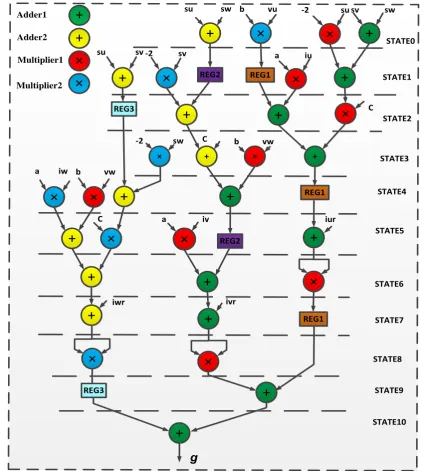
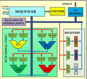
The hard-ware implementation of controller is represented at fig.6. This architecture contains two booth multiplier, two ripple carry adder, 11 multiplexers (mux), 3 registers, etc. Datapath and required arithmetic units are determined based on scheduling diagram and their mapping to the proposed hardware. Sequencer, which is essentially a finite state machine (FSM), provides control signals for the functional units to operate based on the control algorithm. The delay
produced by the hardware, gate drivers and switching devices is inevitable. A simple solution to compensate this delay is to take into account the calculation time and apply the selected switching state after the next sampling instant. Here, the measured currents and the applied switching state at time tk are used to estimate the value of the load currents at time t(k+1). Then, this current is used as a starting point for the predictions for all switching states.
These predictions are calculated by using the load model shifted one step forward in time [17].
Table 1 shows resource usage in fixed-point based architecture for various word-lengths.
×
×
+
+
+
REG1
REG2
×
×
+
STATE0
STATE1
STATE2
STATE3
STATE4
STATE5
STATE6
STATE7
+
×
+
+ ×
×
+
+
×
+
×
×
+
STATE8 REG1
×
×
+
STATE9STATE10
+
sv sw -2 su
b vu su sw
a iu -2 sv
C
-2 sw
b vw
iur
ivr iwr
g
su sv
REG3
b vw
+ C
×
a iw
×
C a iv
REG1
+
REG2
+
+
REG3
+
×
×
+
+
Multiplier2 Multiplier1 Adder2 Adder1
Fig. 5 Arithmetic structure (Scheduling) for computing cost function.
Iranian Journal of Electrical & Electronic Engineering, Vol. 14, No. 1, March 2018 6
COUNTER
F
U
N
C
T
IO
N
A
L
U
N
IT
S
M
U
X
R
3
REGISTERS
CLOCK
M
U
X
R
2
M
U
X
R
1
R
E
G
1
R
E
G
2
R
E
G
3
MUXA2
MUXA2 MUXM2 MUXM2
MUXM1 MUXM1
MUL1 MUL2
ALU1 ALU2
MUXA1 MUXA1
I/O BUFFERS
RESET
IN/OUT
SEQUENCER
SELECTION OF OPTIMAL OUPUT
Fig. 6 proposed low-cost architecture.
Table 1 Required hardware resources.
Word- length 32-bits 24-bits 15-bits
Area (Slices) Multiplier 65 49 34
Adder 33 22 18
5 Implementation Results
This section, evaluates computation accuracy of the implemented fixed-point based architecture for the control system. Digital circuits are implemented on a XILINX Vertex-II Pro development board. The converter parameters are represented in Table 2. DC-link reference is taken as 55V which compared with output DC-link voltage. The error calculated from the reference and output DC voltage is used as an input to PI controller. The reference current is calculated with this PI controller. This reference current is compared with predicted input current for all possible switching states for the active front end rectifier. Hence cost functions are found for 8 valid switching states of the converter; the switching state corresponds to minimum cost function is selected for the next sampling time firing actuation.
Figs. 7-9 display the output voltage under negative load step changes for various word lengths (WL). Every word length consists of integer and fraction parts and one bit is considered as a sign bit. The word length, integer length and fraction length are selected based on the nature of numbers and their corresponding calculations. For word lengths greater than 32 bits, round-off errors have no effect on the outputs accuracy, but the system cost will be increased and calculation
speed will be decreased. For word lengths smaller than 15 bits the outputs are severely erroneous and would not be acceptable. To find an optimal word length, one should consider a tradeoff between the output accuracy and implementation cost of the system. The results for positive load step change are similar to negative step. Here voltage overshoot/undershoot, transition time (TTran), total harmonic distortion(THD) and power factor of input currents are considered as accuracy cost measures. To evaluate performance of the controller negative load current steps are considered. In these states load resistance at t=0.15s changes from 30Ω to
20Ω, 15Ω and 10Ω.
Table 2 Value of the converter parameters.
parameter Value
Vsmax 30v
fs 50Hz
C 1500𝜇f
L 15mH
r 0.4Ω
Vdc* 55v
Ts 40µs
5.1 Word length (WL) is 32 bits
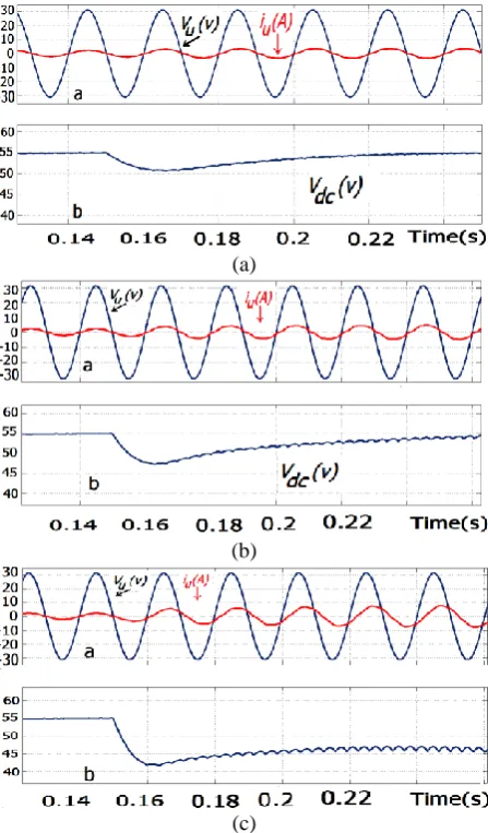
In this case integer length is 12 bits and fraction length is 19 bits. At t=0.15s load resistance changes from 30Ω to 20Ω, 15Ω and 10Ω. For load changing from 30Ω to 20Ω, input current and voltage and output voltage are shown in Fig 7(a) Here THD of input
Iranian Journal of Electrical & Electronic Engineering, Vol. 14, No. 1, March 2018 7 currents are equal, and their values are 3.22%. This
figure reveals the unity power factor because the angle between input voltage and current is zero degree. It can be observed from Fig. 7(a) that undershoot of output voltage is 3.5v and recovery time is 0.05s.
Results for 30Ω to 15Ω are depicted in Fig. (b). It can be observed that undershoot of output voltage is 7v and recovery time is 0.1s. In this case THD of input current is 3.39% and power factor is equal to 1.
In Fig. 7(c) results for load changing from 30Ω to 10Ω are represented. The undershoot of the output voltage is 12v and recovery time is 0.12s. Here THD of the input currents are equal, and their values are 3.5%. The angle between input voltage and current after load changing is 82.2º (power factor=0.13).
5.2 Word length (WL) is 24 bits
In this part for all cases integer length is 10 bits and fraction length is 13 bits. Results for this state are depicted in Fig. 8. It can be observed from Fig. 8(a) that
(a)
(b)
(c)
Fig. 7 Results for WL=32 a) Load changing from 30Ω to 20Ω, b) Load changing from 30Ω to 15Ω and c) Load changing from 30Ω to 10Ω.
for load changing from 30Ω to 20Ω undershoot of output voltage is 4v and recovery time is 0.07s. In this case THD is 4.45% and we observer unity power factor. Input current and voltage and output voltage for load changing from 30Ω to 15Ω are shown in Fig. 8(b). Here THD of the input currents are equal, and their values are 4.55%. This figure reveals the unity power factor. It can be observed that undershoot of the output voltage is 8v and recovery time is 0.12s.
Results for load changing from 30Ω to 10Ω are depicted in Fig. 8(c). In this figure undershoot of output voltage is 13v and recovery time is 0.15s. THD of input current is 4.67% and after load changing the angle between input voltage and current is 84.2º (power factor=0.1).
5.3 Word length (WL) is 15 bits
In Fig. 9 results for this case is represented. Here integer length is 5 bits and fraction length is 9 bits. Similar to another sections at t=0.15s load resistance changes from 30Ω to 20Ω, 15Ω and 10Ω. For load
(a)
(b)
(c)
Fig. 8 Results for WL=24 a) Load changing from 30Ω to 20Ω, b) Load changing from 30Ω to 15Ω and c) Load changing from 30Ω to 10Ω.
Iranian Journal of Electrical & Electronic Engineering, Vol. 14, No. 1, March 2018 8 changing from 30Ω to 20Ω output results are depicted
in Fig. 9(a). In this figure undershoot of output voltage is 5v and recovery time is 0.15s. Here THD of input currents are equal, and their values are 7.15%. The angle between input voltage and current is zero. In Fig. 9(b) results for load changing from 30Ω to 15Ω are represented. Here THD of input currents are equal, and their values are 7.2%. This figure reveals the unity power factor. The undershoot of output voltage is 8v and recovery time is 0.17s.
Results for load changing from 30Ω to 10Ω in Fig. 9(c) are depicted. It can be observed from this figure, that undershoot of output voltage is 13v and recovery time is 0.19s and steady state of output voltage is smaller than 55v. Here THD of input currents are equal, and their values are 7.5%. The angle between input voltage and current after load changing is 85.4º (power factor=0.08).
The results for all cases are represented in Table 3. According to result values for all cases, in smaller WL are the THD, undershoot and recovery time are bigger, so a tradeoff exists between these parameters.
In [13] there is an FPGA design, which is based block-diagram high level synthesis tools (XILINX SPARTAN 3E). In this work word-length is fixed and is 29 bits. In our project we consider various word-length. There is a trade-off between word-length, used resources and output precision, considering gives design flexibility. In other implementations, the controller does not have this flexibility. In previous works by using automated synthesis tools, the software considers many functional units such as adder and multiplier; as a result, the implementation cost increases. But in this work we design a controller with minimum functional units (only two adders and two multipliers). The area on chip of these functional units is variable and dependent on word length.
6 Conclusions
In this article, a low-cost architecture for a digital controller to improve dynamic response of an AC/DC three phase rectifier is presented. For designing this controller we have used predictive control algorithm.
This scheme predicts behavior of future input currents for each switching state of the converter. The cost function appraises predicted value for input currents with their references at the end of each sampling time
(a)
(b)
(c)
Fig. 9 Results for WL=15 a) Load changing from 30Ω to 20Ω, b) Load changing from 30Ω to 15Ω and c) Load changing from 30Ω to 10Ω.
Table 3 Summary of the results for all conditions.
load changing from 30Ω to 20Ω load changing from 30Ω to 15Ω load changing from 30Ω to 10Ω
THD%
P
ower
fac
to
r
Rec
over
y
ti
me
(s)
Undershoot(v)
THD%
Pow
er
fac
to
r
Rec
over
y
ti
me
(s)
Undershoot(v)
THD%
Pow
er
fac
to
r
Rec
over
y
ti
me
(s)
Undershoot(v)
WL=32 3.22 1 0.05 3.5 3.39 1 0.1 7 3.39 0.13 0.12 12
WL=24 4.45 1 0.07 4 4.55 1 0.12 8 4.67 0.1 0.15 13
WL=15 7.15 1 0.15 5 7.2 1 0.17 8 7.5 0.08 0.19 13
Iranian Journal of Electrical & Electronic Engineering, Vol. 14, No. 1, March 2018 9 and minimizes the error between them and then the
optimum switching states apply to power switches. Another concept that has used for controller design is fixed-point computation. The designed hardware is examined in three word lengths to evaluate the computation precision. The main purpose of this design is to minimize the transient time, overshoot/undershoot current and THD of input currents. In this work by using minimal functional unit (low cost architecture) we design a controller that its results show more accuracy in the computation and improvement in the dynamic response of the proposed converter. There is a tradeoff between architecture cost and accuracy of output parameters.
References
[1] A. S. Holter, “Design and Analysis of Stationary Reference Frame Controllers for Active Front End Converter”. MS thesis, NTNU, 2016.
[2] J. R. Rodríguez, J. W. Dixon, J. R. Espinoza, J. Pontt, and P. Lezana, “PWM regenerative rectifiers: state of the art,” IEEE Transactions on Industrial Electronics Vol. 52, pp. 5-22, 2005.
[3] P. Salmeron and S. P. Litrán, “A control strategy for hybrid power filter to compensate four-wires three-phase systems,” IEEE Transactions on Power Electronics, Vol. 25, pp. 1923-1931, 2010.
[4] M. Malinowski, M. P. Kazmierkowski, and A. M. Trzynadlowski, “A comparative study of control techniques for PWM rectifiers in AC adjustable speed drives,” IEEE Transactions on Power Electronics, Vol. 18, pp. 1390-1396, 2003.
[5] S. Kwak, U. Moon, and J. Park, “Predictive-Control-Based Direct Power Control with an Adaptive Parameter Identification Technique for Improved AFE Performance,” IEEE Transactions on Power Electronics, Vol. 29, No. 11, pp. 6178-6187, 2014.
[6] J. Rodriguez, M. P. Kazmierkowski, J. R. Espinoza, P. Zanchetta, H. Abu-Rub, H. A. Young, and C. A. Rojas, “State of the Art of Finite Control Set Model Predictive Control in Power Electronics,” IEEE Transactions on Industrial Informatics, Vol. 9, No. 2, pp. 1003-1016, May 2013.
[7] M. Rivera, J. Rodriguez, B. Wu, J. Espinoza, and C. Rojas, “Current control for an indirect matrix converter with filter resonance mitigation,” IEEE Transactions on Industrial Electronics, Vol. 59, No. 1, pp. 71 –79, Jan. 2012.
[8] M. Rivera, J. Rodriguez, J. Espinoza, T. Friedli, J. Kolar, A. Wilson, and C. Rojas, “Imposed sinusoidal source and load currents for an indirect matrix converter,” IEEE Transactions on Industrial Electronics, Vol. 59, No. 9, pp. 3427 –3435, Sept. 2012.
[9] R. Guzmán, et al., “Finite Control Set Model Predictive Control for a Three-Phase Shunt Active Power Filter with a Kalman Filter-Based Estimation,” Energies, Vol. 10, No. 10, 2017. [10]B. S. Riar, J. Scoltock, and U K. Madawala,
“Model Predictive Direct Slope Control for Power Converters,” IEEE Transactions on Power Electronics, Vol. 32, No. 3, 2017.
[11]A. Hamidi, A. Ahmadi, MS. Feali, S. Karimi, “Implementation of digital FCS-MP controller for a three-phase inverter,” Electrical Engineering, Vol. 97, pp. 25-34, 2015.
[12]S. Vazquez, et al., “Model predictive control for power converters and drives: Advances and trends,”
IEEE Transactions on Industrial Electronics, Vol. 64, No. 2, 2017.
[13]M. P´erez, M. V´asquez, J. Rodr´ıguez and J. Pontt, “FPGA-based predictive current control of a three-phase active front end rectifier,” IEEE International Conference on Industrial Technology, ICIT 2009, pp. 1-6, 2009.
[14]M A. P´erez, RL. Fuentes, J. Rodr´ıguez, “Predictive Control of DC-link Voltage in an Active-Front-End Rectifier,” IEEE International Symposium on Industrial Electronics (ISIE), Gdansk, pp. 1811 – 1816, 2011.
[15] E. Monmasson and M. N. Cirstea, “FPGA design methodology for industrial control systems-A review,” IEEE Transactions on Industrial Electronic, Vol. 54, No. 4, pp. 1824–1842, Aug. 2007.
[16]Y. Kung, R. Fung, and T. Tai, “Realization of a motion control IC for X-Y table based on novel FPGA technology,” IEEE Transactions on Industrial Electronic, Vol. 56, No. 1, pp. 43–53, Jan. 2009.
[17]P. Cortes, J. Rodriguez, C. Silva, and A.Flores, “Delay Compensation in Model Predictive Current Control of a Three-Phase Inverter,” IEEE Transactions on Industrial Electronics, Vol. 59, No. 2, Feb. 2012.
A. Hamidi was born in Aleshtar, Iran, in 1980. He received the B.Sc. degree in electronic engineering from Shahid Rajaee University, Tehran, Iran, in 2002, and the M.Sc. degree in electronic engineering from the Department of Electrical Engineering, Razi University, Kermanshah, Iran, in 2007, where he is currently a Ph.D. student of electronic engineering, Razi University. From 2016 to 2017, he was a visiting scholar at the University of Windsor, Canada. His current research interest includes hardware implementation of signal processing systems, high-level synthesis, analog and digital electronic circuit design and optimization, and artificial neural networks.
Iranian Journal of Electrical & Electronic Engineering, Vol. 14, No. 1, March 2018 10
A. Ahmadi received the B.Sc. and M.Sc. degrees in electronics engineering from the Sharif University of Technology and Tarbiat Modares University, Tehran, Iran, in 1993 and 1997, respectively, and the Ph.D. degree in electronics from the University of Southampton, U.K., in 2008. He was with Razi University, Kermanshah, Iran, as a Faculty Member. From 2008 to 2010, he was a Fellow Researcher with the University of Southampton. He is currently an Associate Professor in the Electrical Engineering Department, Razi University and visiting scholar at the University of Windsor, Canada. His current research interest includes neuromorphic, hardware implementation of signal processing systems, bio-inspired computing, memristors and hardware security.
S. Karimi was born in Kermanshah, Iran, in 1972. He received the B.S. degree from University of Tabriz, Tabriz, Iran, in 1995, the M.S. degree from Sharif University of Technology, Tehran, Iran, in 1997, and the Ph.D. degree in electrical engineering from the Université Henri Poincaré, Nancy, France, in 2008. He is currently an
Assistant Professor with Department of Electrical
Engineering, Faculty of Engineering, Razi University, Kermanshah, Iran. His research interests are active power filters, power quality, FACTS Devices and fault tolerant converters.