International Journal of Advanced Engineering, Management and Science (IJAEMS) [Vol-2, Issue-8, August- 2016] Infogain Publication (Infogainpublication.com) ISSN : 2454-1311
www.ijaems.com Page | 1332
Implementation of a three Phase Inverter with a
Front End Diode Rectifier Using Average Model
Parvathi M. S
1, Nisha G. K
21PG Scholar, Department of EEE, Kerala University, India
2
Associate Professor, Department of EEE, Kerala University, India
Abstract— As technology grows every day, the study of
power systems has shifted its direction to power electronics to produce the most efficient energy conversion. Power electronics is the study of processing and controlling the flow of electric energy by supplying voltages and currents in a form that is suited for user loads. A power electronic system is any technical system which is an assembly of components such as AC to DC converters (rectifiers) and DC to AC converters (inverters), that are connected together to form a functioning machine or an operational procedure. The paper presents the implementation of a three phase inverter with a front end diode rectifier. The components are modeled separately using the state space average method.
Keywords— Average Model, Front end diode rectifier and Three phase inverter.
I. INTRODUCTION
Today, power electronics is a rapidly expanding field in electrical engineering and a scope of the technology covers a wide spectrum of electronic converters. Different kinds of power supplies are used everywhere in normal daily routines in both at home, office work or in an industrial environment. This is due to the progress in electronic components and equipment development that has been achieved in the last few decades. A power electronic system assembles rectifiers that convert ac to dc with the adjustment of voltage and current and inverters which produce ac of controllable magnitude and frequency [1].
In the case of a polyphase rectifier, the phase-shifted pulses overlap each other which produce a smoother dc output than that made by a single-phase ac rectifier [2]. The modeling of single phase, three phase rectifiers and suitable controller design for the modeled rectifier circuit is presented in [3]. In [4] the authors have presented a comparative study on the average model of diode rectifier with the model developed by modified nodal analysis method. For the analysis and controller design purpose in inverters, the average modeling method is found to be an effective method [5] – [7]. The modified nodal analysis method and the state space average method in the
modeling of a three phase inverter is discussed in [8]. Conventional switching models and state-space averaging methods which take dead-time effects into consideration have been applied successfully in the inverters [9], [10]. This paper presents the implementation of a three phase inverter using a front diode rectifier. The section II gives the average model of a three phase diode bridge rectifier. The section III gives the average model of a three phase inverter. The section IV explains the implementation of the three phase inverter with a front end diode rectifier and the section V discusses the results and simulations.
II. AVERAGE MODEL OF A THREE PHASE
DIODE RECTIFIER
In order to make prime decisions in the design procedures, power electronic modeling methods are widely used. The modeled circuit helps to determine the performance of the circuit along with the component values as well. State space average modeling method is a common technique that is utilized to obtain models of power electronic circuits, for ac and dc power conversions. The main advantage of this particular method is that the accuracy can be increased and ripple free waveforms can be obtained.
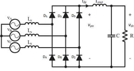
A simplified three phase diode bridge rectifier is shown in the Fig. 1. The circuit consists of three ac input sources (VA, VB and VC), input source reactor (Ls), diodes (D1 to D6), output inductance (Lout), output filter capacitance (C) and resistance (R) which represents the load on the rectifier [11].
International Journal of Advanced Engineering, Management and Science (IJAEMS) [Vol-2, Issue-8, August- 2016] Infogain Publication (Infogainpublication.com) ISSN : 2454-1311
www.ijaems.com Page | 1333
Utilizing the general state space averaging method, the switching functions sa, sb and sc for a three phase diode bridge rectifier can be expressed by a Fourier series using the first harmonic terms of the series as shown in the equation (1).
=2 ∗ √3 sin sin −23 sin +23 (1)
The average dc output voltage Vpn can be expressed as the equation (2). = ∗ = !"∗#$#% + % (2)
Also, the dc current equation can be obtained as shown in equation (3). $% = &## +% ' (3)%
From the equation (2), the left hand side of the equation can be expanded as: ∗ = ()* =2 ∗ √3 ∗ +( ∗ ) + ( ∗ ) + ( ∗ ), (4)
Now, the right hand side of the equation (2) can be solved using the Transient simulation method. In this method, the differential current equation can be converted to its equivalent Forward Euler form and solved to obtain the value for the (n+1)th value of the dc current. .ℎ = 0 !"∗$% 12− $ % ℎ 3 + % (5)
From the equation (5), the (n+1)th value of the dc current can be calculated as: $%12= ℎ !"∗ 5.ℎ − ($% ∗ ')6 + $% (6)
where, ‘h’ is the delta constant value or the time step. Similarly, from the equation (3), the differential voltage equation can be converted to its equivalent Forward Euler form and solved to obtain the value for the (n+1)th value of the dc voltage. $% = & ∗ 0 % 12− % ℎ 3 + ' (7)%
Thus, from the equation (7), the (n+1)th value of the dc voltage can be calculated as: %12= & ∗ 5$ℎ %12− ( % /')6 + % (8)
The modeling equation for a three phase diode bridge rectifier is obtained using the average state space model and the transient simulation techniques. The main modeling equations are equation (4), (6) and (8). III. AVERAGE MODEL OF A THREE PHASE INVERTER In the study of inverters and their dynamic performance, various switching models are obtained based on the switching conditions, as in the Modified Nodal Analysis method explained earlier in the chapter, which is feasible for a single inverter or a small scale inverter system. Therefore, in case of large scale inverter systems, switching models becomes complicated. Hence, a state space averaging method is formulated which is effective for the analysis and controller design purpose in inverters. However, it is yet to give guaranteed high accuracy performance. A generalized state space averaging model is considered which enhances the fundamental voltage and current calculation with desired accuracy and precision. At the same time, this method enables the steady state as well as transient analysis processes [12]. The circuit diagram of a 3 phase 3 wire Voltage source inverter is as shown in the Fig. 2. Fig. 2: Circuit diagram of a three phase three wire voltage source inverter In the Fig. 2, assuming that the loads are 3 phase symmetrical resistive loads in delta connection, whose value are R, we obtain the equations from (9) to (14). = − = #($#− $ )+ ;<($ − $ ) + => (9)
= − = #($#− $ )+ ;<($ − $ ) + >@ (10)
= − = #($#− $ )+ ;<($ − $ ) + @= (11)
$ = &## +=> ' 1 => (12)
$ = &## +>@ ' 1 >@ (13)
$ = &## +@= 1' @= (14)
where, $ , $ , $ are virtual line currents which can be calculated as mentioned in the equations from (15) to (20). $ = $ − $ (15)
International Journal of Advanced Engineering, Management and Science (IJAEMS) Infogain Publication (Infogainpublication.com
www.ijaems.com
$ = $ − $
$ 13 $ $
$ 13 $ $
$ 13 $ $
Similar to the equation (2) in the modeling of three phase diode bridge rectifier by the average model, it can be written that:
. %
. %
. %
Thus, the conventional state equations of three phase inverter can easily be constructed.
#$
# ;<$ 31 => 3 1
#$
# ;<$ 31 >@ 3 1
#$
# ;<$ 31 @= 3 1
# => # '&1 => 1& $ # >@ # '&1 >@ 1& $ # @= # '&1 @= 1& $ The differential voltage and current equations can be converted to its equivalent Forward Euler form and substituting the equations (21) to (23) in the Forward Euler equations we obtain the value for the (n+1) of the corresponding ac voltage and ac current. $ 12 / ∗ ;<$ 1 3 => 31 $ 30
$ 12 / ∗ ;<$ 1 3 >@ 31 $ 31
$ 12 / ∗ ;<$ 1 3 @= 31 $ 32
=>12 & $/ => >@12 /& $ >@ @=12 /& $ @= The switching function is given by: sD m2 cos ωt ∅D 1 2 where k = a, b, c ; m is the modulation ratio taken as 0.5 ∅J ∅K , ∅L ∅K MNπ , ∅O ∅K MNπ; where initial phase angle. International Journal of Advanced Engineering, Management and Science (IJAEMS) [Vol Infogainpublication.com) 17 18 19 20
modeling of three phase e model, it can be 21
22
23
Thus, the conventional state equations of three phase 24 25 26 27 28 29
The differential voltage and current equations can be converted to its equivalent Forward Euler form and substituting the equations (21) to (23) in the Forward ue for the (n+1)th value of the corresponding ac voltage and ac current. . % . % . % 33 34 35 36 where k = a, b, c ; m is the modulation ratio taken as 0.5
; where ∅K is the
IV. IMPLEMENTATION
The block diagram for the implementation of a three phase inverter with a front end diode rectifier is as shown in the Fig. 3.
Fig. 3: Block diagram of three phase inverter with a front end diode rectifier
In the block diagram, the three phase diode rectifier by a three phase ac supply R, Y and B. The diode rectifier converts the ac supply to dc values. The nodes 1 and 2 at the output of the rectifier, represents the dc voltage and dc current values respectively. The three phase inverter is used to convert the dc values to ac values. Therefore, the output dc voltage value of the diode rectifier is given as input to the three phase inverter. The ac voltage and current values are obtained at the output side of the three phase inverter. The nodes 3, 4 and 5
ac phase currents and the nodes 6, 7 and 8 represent the output ac phase voltage values of the three phase inverter fed by a front end diode rectifier.
V. RESULTS AND DISCUSSIONS
The waveforms for the implementation of a three phase inverter with a front end diode rectifier are
graphs include the three phase supply input, the diode rectifier output and the output voltage and current values of the three phase inverter.
for the average model of three phase diode bridge rectifier are as shown in the Table 1.
Table 1: Parameters for simulation of diode rectifier in average model
SYMBOL PARAMETERS
Vabc Input Voltage
f Fundamental frequency
L Filtering Inductor
C Filter Capacitor
R Load Resistance
h Time step
The Fig. 4 shows the three phase input supply voltage (415 V, 50 Hz) given to the diode rectifier.
[Vol-2, Issue-8, August- 2016] ISSN : 2454-1311
Page | 1334 IMPLEMENTATION
agram for the implementation of a three phase inverter with a front end diode rectifier is as shown
Fig. 3: Block diagram of three phase inverter with a front end diode rectifier
In the block diagram, the three phase diode rectifier is fed by a three phase ac supply R, Y and B. The diode rectifier converts the ac supply to dc values. The nodes 1 and 2 at the output of the rectifier, represents the dc voltage and dc current values respectively. The three phase inverter is ert the dc values to ac values. Therefore, the output dc voltage value of the diode rectifier is given as input to the three phase inverter. The ac voltage and current values are obtained at the output side of the three phase inverter. The nodes 3, 4 and 5 represent the output currents and the nodes 6, 7 and 8 represent the voltage values of the three phase inverter fed by a front end diode rectifier.
RESULTS AND DISCUSSIONS
The waveforms for the implementation of a three phase inverter with a front end diode rectifier are obtained. The graphs include the three phase supply input, the diode rectifier output and the output voltage and current values The parameter specifications for the average model of three phase diode bridge rectifier
Parameters for simulation of diode rectifier in average model
PARAMETERS VALUE UNIT
Input Voltage 415 V
Fundamental frequency 50 Hz
Filtering Inductor 0.05 H
Filter Capacitor 0.05 F
Load Resistance 2 Ω
Time step 100 µs
International Journal of Advanced Engineering, Management and Science (IJAEMS) Infogain Publication (Infogainpublication.com
www.ijaems.com Fig. 4: Three phase supply to the Diode rectifier (415V,
50Hz) (X axis: 1 unit = 0.1s and Y axis: 1 unit = 200V)
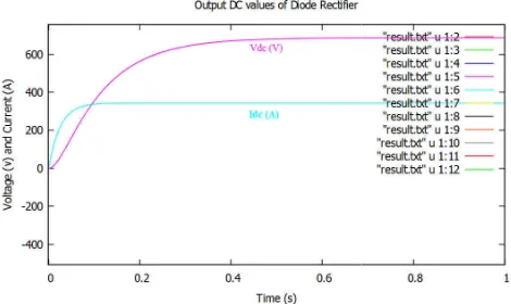
The Fig. 5 shows the output dc voltage and current values of the diode rectifier obtained at the nodes 1 and 2 respectively, with the specified modeling parameter specifications.
Fig. 5: Output dc voltage and dc current of a 3 phase rectifier ,Vdc = 687 V and Idc = 343 A (X axis: 1 unit = 0.2s and Yaxis: 1 unit = 200 units of voltage and current)
The parameter specifications for the average model of three phase inverter are as shown in the Table
Table 2: Parameters for simulation of inverter in average method
SYMBOL PARAMETERS VALUE
Vdc
Input Voltage (output of the diode rectifier) m Modulation Ratio
f Fundamental frequency
φ0 Initial phase angle L Filtering Inductor
rL
ESR of filtering
inductor 1.245 C Filter Capacitor
R Load Resistance h Time step
The simulation waveform for phase currents at the output of the inverter is as shown in the Fig. 6. The figure shows
International Journal of Advanced Engineering, Management and Science (IJAEMS) [Vol
Infogainpublication.com)
to the Diode rectifier (415V,
50Hz) (X axis: 1 unit = 0.1s and Y axis: 1 unit = 200V)
The Fig. 5 shows the output dc voltage and current values of the diode rectifier obtained at the nodes 1 and 2 respectively, with the specified modeling parameter
Fig. 5: Output dc voltage and dc current of a 3 phase = 343 A (X axis: 1 unit = 0.2s and Yaxis: 1 unit = 200 units of voltage and current)
The parameter specifications for the average model of are as shown in the Table 2.
of inverter in average
VALUE UNIT
687 V
0.6 -
50 Hz
0 rad/s 1.0 mH
1.245 Ω
1.0 mF
10 Ω
100 µs
The simulation waveform for phase currents at the output . The figure shows
the ac phase currents with a magni nodes 3, 4 and 5 (as in Fig. 3).
Fig. 6: Output phase current waveform with a magnitude 143 A (X axis: 1 unit = 0.2s and Y axis: 1 unit = 10 A)
The simulation waveform for phase voltages at the output of the inverter is as shown in the Fig. 7
the ac phase voltages with a magnitude of (2V V) for the given input dc of 687
(as in Fig. 3).
Fig. 7: Output phase voltage waveform with a magnitude 458 V for the dc input of 687 V (X axis: 1 unit = 0.1s and
Y axis: 1 unit = 200 V)
VI. CONCLUSION
The paper presents the implementation of a three phase inverter with a front end diode rectifier. The modeling of the three phase diode bridge rectifier and the three phase inverter are done using the generalized state space average method. The three phase inverter is fed from the output dc values of the diode rectifier. The output waveforms of the average model of the d
rectifier and the inverter are obtained.
advantage of the average model of three phase diode rectifier and three phase inverter is that the it gives continuous and ripple free waveforms.
[Vol-2, Issue-8, August- 2016] ISSN : 2454-1311
Page | 1335
currents with a magnitude of 143 A at the nodes 3, 4 and 5 (as in Fig. 3).
Fig. 6: Output phase current waveform with a magnitude 143 A (X axis: 1 unit = 0.2s and Y axis: 1 unit = 10 A)
simulation waveform for phase voltages at the output verter is as shown in the Fig. 7. The figure shows the ac phase voltages with a magnitude of (2Vdc/3 = 458 687 V at the nodes 6, 7 and 8
tput phase voltage waveform with a magnitude 458 V for the dc input of 687 V (X axis: 1 unit = 0.1s and
Y axis: 1 unit = 200 V)
CONCLUSION
International Journal of Advanced Engineering, Management and Science (IJAEMS) [Vol-2, Issue-8, August- 2016] Infogain Publication (Infogainpublication.com) ISSN : 2454-1311
www.ijaems.com Page | 1336 REFERENCES
[1] Agrawal, J.P., Power Electronic Syatems: Theory
and Design, Upper Saddle River, NJ: Prentice Hall,
2001.
[2] Rashid-Muhammad, H., Power Electronics Circuits,
Devices, and Applications, New Jersey: Pearson
Prentice Hall, 2004.
[3] Nagisetty-Sridhar and R. Kanagaraj, Modeling and
Simulation of Controller for Single Phase and Three Phase PWM Rectifiers. Indian Journal of Science and
Technology, 2015. 8(32).
[4] Shilpa-George and A.S. Shajilal, Comparitive Study
of Average Model of Diode Rectifier with the Model Developed by Modified Nodal Analysis Method. The
International Journal of Science and Technoledge, 2016. 4(7): p. 203-208.
[5] Runxin-Wang and Jinjun-Liu, Redefining a
New-Formed Average Model for Three-Phase Boost Rectifiers/Voltage Source Inverters. The 24th
Applied Power Electronics Conference and
Exposition, 2009. p. 1680-1686.
[6] M. Davari, A.R. Pourshoghi, I. Salabeigi, G.B.
Gharehpetian and S.H. Fathi, A New Nonlinear
Controller Design Using Average State Space Model of the Inverter-Based Distributed Generation to Mitigate Power Quality Problems. International
Conference on Electronic Machines and Systems, 2009. p. 1-5.
[7] N. Kroutikova, C.A. Hernandez-Aramburo and T.C.
Green, State-space model of grid-connected inverters
under current control mode. The Institution of
Engineering and Technology, 2007. 1(3): p. 329- 338.
[8] Parvathi M.S. and Nisha G.K., Comparison on the
Average Model of a Three Phase Inverter with its Modified Nodal Analysis Method. International
Journal of Current Engineering and Scientific Research (IJCESR), 2016. 3(7): p. 65-70.
[9] Toni-Itkonen and Julius-Luukko,
Switching-Function-Based Simulation Model for Three-Phase Voltage Source Inverter Taking Dead-Time Effects into Account. The 34th IEEE Annual Conference on
Industrial Electronics, 2008. p. 992-997.
[10] S. Ahmed, Z. Shen, P. Mattavelli, D. Boroyevich, M. Jaksic, K. Kamiar and J. Fu, Small-Signal Model
of a Voltage Source Inverter (VSI) Considering the Dead-Time Effect and Space Vector Modulation Types. The 26th Applied Power Electronics
Conference and Exposition, 2011. p. 685-690.
[11]Joseph-Maurio, Thomas-Roettger and
Matthew-Superczynski, Average model of a three phase
controlled rectifier valid for continuous and discontinuous conduction modes. Transportation
Electrification Conference and Expo (ITEC), 2015. p. 1-7.
[12]Zhao-Lin and Hao-Ma, Modeling and Analysis of
Three-phase Inverter based on Generalized State Space Averaging Method, IEEE Annual Conference