Technology (IJRASET)
Implementation of Optimized 64 Bit MAC using
Vedic Multiplier and Reverse Logic Gate
Savitha S1, S. Raja2, Amrutha Soroobini S3, Anusruthi K4, Barani Priya L5, Gnana Anu Rekha M6 1,2
Assistant Professor, 3,4,5,6UG Students , Dept. of ECE Sri Shakthi Institute of Engg and Technology, Coimbatore, TN, India.
Abstract: In advanced digital signal processing the MAC (multiply and accumulate unit) unit acquires the predominant role. The optimized MAC unit deals with improvising the speed, area power consumption. The high speed processors rely on multiplication operation as they are the core of many DSP applications today. The multiplication is done using the ancient Vedic multiplication and the addition is carried out by reversible logic gate. The Vedic multiplier is used so as to reduce the partial product generation and reduces the latency. Reversible logic is used to reduce the power dissipation and to resist information loss. The carry select adder is used as it is the fastest addition adder and the speed is due to the limited carry propagation from input to output. The optimization of MAC unit design is programmed using Verilog - HDL using Xilinx ISE 14.7 and the FPGA implementation is done on Spartan3E.
Keywords: MAC, reversible logic gate, carry select adder.
I. INTRODUCTION
The MAC unit is to provide a physically compact, good speed and a low power consumption chip. The MAC unit has been extensively used in DSP, high speed processors for applications like filtering, signal conditioning etc. In order to improve the MAC unit speed, the partial product generation has to be reduced and the accumulator block usage has to be limited. The Vedic multiplication technique is used for the fastest operation with less partial propagation. Vedic maths tricks enhance the calculation 10 to 15 times than the usual method. Among the Vedic arithmetic the Vedic multiplication is used in the design of MAC.The Vedic multiplication is based on the following sutras.
Technology (IJRASET)
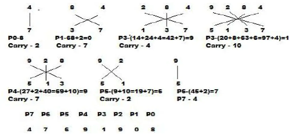
Figure 1 Multiplication of two numbers Using Urdhva Triyakbhyam Sutra
(Note here the maximum number of digits is 4). ((4*5) + (8*1) + (2*3) + (9*7) =97). The result should be added with the carry of the previous stage. 97+4= 101. Now the special case of carry can be seen, where the carry is 10, which means at the end of each stage only one digit can be passed to the sum and all other digits considered as carry. The next stage 5 involves the multiplication of numbers now with taken 3, but with the reverse order starting from the right side. (9*3)+ (2*1) + (8*5) = 69. The carry was 10 so result will be 79, with 7 carry and 9 as the fifth digit in sum. The stage 6 involves two digits taken at a time (9*1) + (5*2) = 19 carry added will be 7, so the result is 26. The carry at this stage is 2 and 6 becomes the sixth digit of the sum. The stage 7 also the last stage involves most significant bit of both the numbers to be multiplied. (9*5) = 45. Add the carry; the result is 45+2=47. The 4 and 7 becomes the seventh and eight digit of the sum. The result obtained in the last stage will directly become the most significant bits of the final sum. The multiplication of two 4 digit numbers requires 8 stages of calculation yielding 8 digit of final sum.
Reversible logic has been derived from thermodynamics of information processing. The Reversible logic is gathering importance in areas of CMOS design because it has low power dissipation. The traditional circuits consisting of irreversible gates like AND, OR, XOR dissipates power as heat due to which the loss of information during computation occurs. In order to sort out this information loss the traditional circuits are designed with the help of reversible logic. In order to attain gate reversible, additional input and output lines are added so that a one to one mapping exists between the input and output. This avoids the information loss that is the main factor behind information loss in irreversible circuits. In the reverse logic, the number of inputs will be equal to the number of outputs. Hence power dissipation will be reduced by using reverse logic. This paper is organized as follows. Section II discusses literature survey. Section III describes the existing work of MAC architecture. The proposed model of MAC architecture with built in reversible logic gate is discussed in section IV. The FPGA prototyping and experiment results will be presented in section V. Finally, conclusions are drawn.
II. LITERATURE SURVEY
Technology (IJRASET)
Proposed that the reversible logic is used to minimize the power dissipation that occurs in traditional circuits by preventing the information loss. Therefore the classical circuits are designed using reversible logic. The two main constraints of reversible logic circuit is
Fan out not allowed
Feedbacks or loops not allowed.
III. EXISTING METHOD
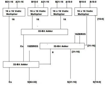
The MAC unit is the hardware that performs the product of two numbers and stores the result in the accumulator register. The 32 bit multiplier and 32 bit multiplicand are multiplied together to provide 64 bit output which is illustrated using the fig 2.
Fig 2. 32*32 Vedic Multiplier using 16*16 Vedic multiplier
The multiplicand and the multiplier are multiplied using the Vedic multiplication sutra, the computation becomes 10 - 15 times faster than usual multiplication. The shift operation is not required as urdhava tribhayam sutra is used. The partial products are generated using vertical and crosswise computation. The addition is performed using the carry select adder such that the fast addition of partial product is obtained. The Reversible logic adder is used due to its property of low power consumption. The information loss is also reduced due to low power dissipation finally, the product obtained is stored in the accumulator block. The
accumulator stores the result in the form of the result is stored in the A register. The delay is reduced by reducing the time of carry propagation. The efficient multiplier is designed using the Vedic multiplier and reversible logic adder.
IV. PROPOSED SYSTEM
[image:4.612.131.481.201.483.2]Technology (IJRASET)
The 64 x 64 Vedic multiplier has been designed using the hierarchical method. The design process of 64 X 64 bit Vedic multiplier requires the lower bit level of 34x34 bit Vedic multiplier. Similarly, 32X32 bit multiplier requires lower level bit of 16X16 Vedic multiplier. Therefore it is simple to build the multiplier architecture to the higher level by maintaining its modularity. The architecture requires the intermediate adder block. The adder block is the reversible logic adder design. The two number A and B are applied in the crosswise order. The inputs consists of 64 bit and final product will be maximum of 128 bit. The logic behind the operation of the MAC design is the multiplicand which is of 64 bit is split into two halves each of 32 bit. The input to the first stage of multiplier will be lower halve of both the numbers, second and third stage will be swapped halves of the two and the final and fourth stage will be the upper half of the numbers. The multiplication operation is followed by the addition operation which can add 64 bit numbers and the sum will be saved, the carry if generated will be added to the next successive stages and so on. The adder will be appended with zeros to one of the input in order to equate the number of bits so as the addition operation can be performed without any error. The adder is responsible to provide the carry 0f the last
Stage where the output of the last stage adder is considered as the sum. The LSB sum bits will be directly taken from the first stage of the multiplier. The architecture has the 32 bit multiplier whose architecture is the photocopy of the 64 bit multiplier except the difference is the 32 bit architecture consists of the inputs to be 32 bits and the Reversible adder of 32 bit. CA in the
Architecture refers to the carry generated in that particular stage of operation.
In the MAC unit it is very necessary to have a very fastest acting multiplier and a very efficient adder (the adder is initially set to zero) as it has the critical unit on the data-path. The result of multiplication and the addition of partial products give the result which will be stored in the Accumulator. The next level in the design will be the 4 bit Vedic multiplier design. It requires the 2x2multiplier design, the input multiplicands will have maximum of 4 bit which ranges from0000, 0001, 0010………..1111. The output produced will be of 8-bit, the Vedic multiplier improvised algorithm states that the Vedic multiplier should have 4 input multiplier where the inputs will be applied in the vertical and crosswise order. The 64x64 multiplier design has the 32x32 Vedic multiplier design. The logic of the block diagram remains the same based on the improvised Vedic Sutra. Here both the multiplicand will be of 64 bits. (m=64). The multiplicands have to be divided into 2 according to the improvised algorithm.
The result of the 32x32 multiplication will be maximum of 64bits. The inputs A and B are divided into two halves each of 32 bits (m/2). The 64 bit multiplier input ranges from 64‟B0, 64‟B1 ………64‟B63 input the adder or subtract or can be selected. If input A=0, the proposed gate works as a reversible Full adder, and if input A=1, then it works as a reversible Full subtract or. select ROI in the dialog shown with any of the tools click ok .Finally see the result in image control panel.
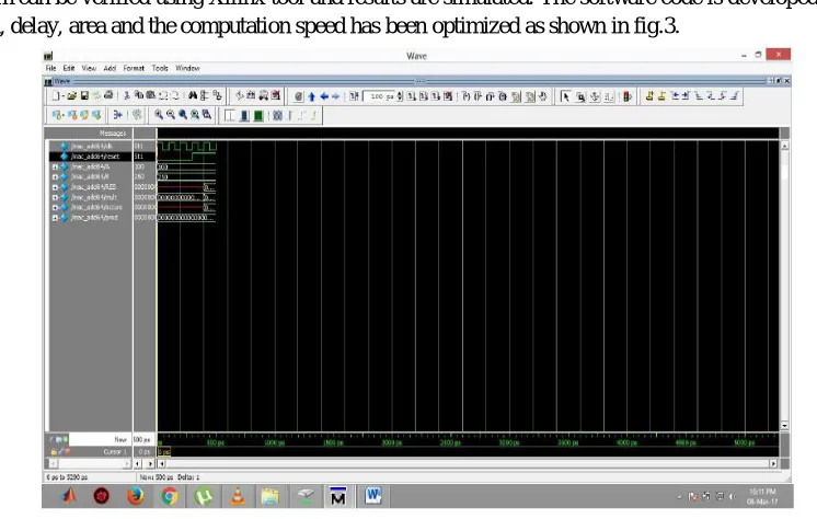
V.RESULTSANDDISCUSSIONS
[image:5.612.120.493.460.697.2]Technology (IJRASET)
. VI. CONCLUSION
An MAC unit software prototype based on Vedic multiplication and reversible logic was presented and simulated. The Proposed work more efficiently with fault detection. As far as the future work is concerned, the prototype can be extended with fault recovery technique. The delay is reduced from nano seconds to pico seconds. The area occupied by higher level.
REFERENCES
[1] JayaKumar.S, Sivaramakrishnan, Venketesan.k, Vaithiyanathan (2013) ‘Simulation And Implementation Of Vedic Multiplier Using VHDL Code’,
International Journal of Scientific & Engineering Research Volume 4, Issue 1, January-2013 ISSN 2229-5518.
[2] Anitha.R, Neha Deshmukh Mesman, Prashant Agarwal, Sarat Kumar Sahoo,Kathikeyan, Prabhakar.S (2015) ‘A 32 BIT MAC Unit Design Using Vedic
Multiplier and Reversible Logic Analysis of Resource Arbitration’, 2015 International Conference on Circuit, Power and Computing Technologies [ICCPCT].
[3] Ponni.M, Lekshmi Viswanath.M (2012) ‘Design and Analysis of 16 Bit Reversible AL Analysis’, IOSR Journal of Computer Engineering (IOSRJCE) ISSN :
2278-0661 Volume 1, Issue 1 (May-June 2012), PP 46-53.