Technology (IJRASET)
©IJRASET: All Rights are Reserved
408
Closed Loop Control for Fast Varying Dynamic
Load with Transient Free TBSC Compensator
Khushal Shende1, D.R.Patil2, S.D.Patil3, Sumant Lokhande41,2
Electrical Engineering Department,WCE sangli
3,4
Electrical Engineering Department,ADCET Ashta
Abstract— Topology for reactive power compensation suitable for dynamic loads in closed loop is presented. The scheme consists of Thyristor Binary Switched Capacitor (TBSC) banks. TBSC is based on a chain of Thyristor Switched Capacitor (TSC) banks arranged in binary sequential manner. A transient free switching of TBSCs is carried out. Proposed topology allows step less reactive power compensation for dynamic loads in very fast responding closed loop. Simulation results show that the proposed scheme can achieve reactive power compensation cycle to cycle basis and the harmonics contents of source are maintained at insignificant levels due to filtering action of TBSC.
Keywords— Reactive power compensation, TBSC, transient free switching Binary Current Generation Binary Sequential mode of operation.
I. INTRODUCTION
It is well documented in literature and through public discussions at various levels that a substantial power loss is taking place in our low voltage distribution systems on account of poor power factor, due to inadequate reactive power compensation facilities and their improper control. Switched LT capacitors can directly supply the reactive power of loads and improve the operating condition. Government of India has been insisting on shunt capacitor installations in massive way and encouraging the state electricity boards through Rural Electrification Corporation and various other financing bodies [1, 2].The expansion of rural power distribution systems with new connections and catering to agricultural sector in wide spread remote areas, giving rise to more inductive loads resulting in very low power factors. The voltages at the remote ends are low and the farmer’s use high HP motors operating at low load levels with low efficiencies. This is giving rise to large losses in the distribution network Thus there exists a great necessity to closely match reactive power with the load so as to improve power factor, boost the voltage and reduce the losses.
The conventional methods of reactive power supply are through switched LT capacitors, mostly in equal steps in various automatic power factor controllers developed by number of companies. In this paper, a more reliable, technically sound, fast acting and low cost scheme is presented by arranging the contactor switched capacitor units in five binary sequential steps. This enables the reactive power variation with the least possible resolution. In addition a thyristor controlled reactor of the lowest step size is operated is conjunction with capacitor bank, so as to achieve continuously variable reactive power. As there is reduction in loss with shunt compensation in the feeders, the efficiency increases and conservation of energy takes place. Besides the enhancement transformer loading capability the shunt capacitor also improves the feeder performance, reduces voltage drop in the feeder and transformer, better voltage at load end, improves power factor, improves system security with enhanced utilization of transformer capacity, gives scope for additional loading, increases over all efficiency, saves energy due to reduced system losses, avoids low power factor penalty, and reduces maximum demand charges.
In this paper, a more reliable, technically sound, fast acting and low cost scheme is presented by arranging the thyristor switched capacitor units in five binary sequential steps. This enables the reactive power variation with the least possible resolution. As there is reduction in loss with shunt compensation in the feeders, the efficiency increases and conservation of energy takes place. Besides the enhancement of transformer loading capability the shunt capacitor also improves the feeder performance, reduces voltage drop in the feeder and transformer, better voltage at load end, improves power factor and improves system security, increases over all efficiency, saves energy due to reduced system losses, avoids low power factor penalty, and reduces maximum demand charges.
II. DESIRABLEFEATURES
The desirable features of the proposed scheme are as follows:
A. It maintains the power factor at the PCC to any specified value.
Technology (IJRASET)
C. Maximum compensation time is 20 msec.
D. No transients or harmonics are allowed to be present due to fast selective instants of switching in well co-ordinate manner.
E. It is adaptive in the sense that the amount of the compensation is determined and provided on a cycle by cycle basis.
F. Capacitors are sized in binary sequential ratio for minimum size of switching steps.
G. The control strategy is error activated to match with the load reactive power for the chosen time interval.
H. It is flexible to choose required number of steps as per the resolution
III. PROPOSEDTOPOLOGYDESCRIPTION
This paper presents a simple topology, which is shown in Fig.1. The proposed scheme consists of Thyristor Switched Capacitor (TSC) banks in binary sequential steps known as Thyristor Binary Switched Capacitor (TBSC).
Distribution
Transformer
Point of Common Coupling(PCC) 3 Phase, 50Hz, 440V, Bus Bar
Mocrocontroller for Switching Capacitor Bank
Dynamic Load 11Kv/440v
TH1 TH2 TH3 TH4
in Binary Sequential Mode of Operation S0
S1 S2 S3 S4
V
I
TH0-TH1 - Thyristor
L0-L1 - Current Limiting Reactor C0-C1 - Capacitor C.T - Current Transformer P.T - Potential Transformer
S0-S1 - Switching Signals
L0 L1 L2 L3 L4
C0 C1 C2 C3 C4
[image:3.612.42.548.223.484.2]TH0
Technology (IJRASET)
©IJRASET: All Rights are Reserved
410
This TBSC facilitates stepless control of reactive power closely matching with load requirements so as to maintain desired power factor. The proposed topology has following distinctive features:TSC banks are arranged in Binary sequential steps to provide almost continuous reactive power compensation.
Transient free switching is obtained by pre-charging the capacitors to the negative/positive peak of supply voltage and firing the thyristors at the negative/positive peak of supply voltage.
It compensates for rapid variation in reactive power.
Reactive power compensation is achieved in cycle by cycle basis.
At the distribution transformer requiring total reactive power Q for improving the power factor from some initial value P.f1 to the desired value P.f2 at the load. This Q can be arranged in binary sequential ‘n’ steps, satisfying the following equation:
Q = 2nC + 2n−1C + ... + 22C + 21C + 20C
The schematic diagram of the capacitor bank in five binary sequential steps through contactors and with respective current limiting reactors is shown in Fig.1 TBSC. The operating principle of each equipment is analyzed in the following sections.
A. TBSC
TBSC consists of an anti-parallel connected thyristor and diode as a bidirectional switch in series with a capacitor and a current limiting small reactor. Transient free switching of capacitors is obtained by satisfying following two conditions
1) Firing the thyristors at the negative/positive peak of supply voltage
2) Precharging the Capacitors to the negative/positive peak of supply voltage
TSC current is sinusoidal and free from harmonics, thus eliminating the need for any filters. Small-series inductor is placed in series with capacitor. It serves following purposes
1) It limits current transients during overvoltage conditions and when switching at incorrect instants or at the inappropriate voltage polarity.
2) The chosen inductor magnitude gives a natural resonant frequency of many times the system nominal frequency. This ensures that the inductance neither creates a harmonic-resonant circuit with the network nor dampers.
In the proposed paper capacitor bank step values are chosen in binary sequence weights to make the resolution small. If such ‘n’ capacitor steps are used then 2n different compensation levels can be provided [6]. In this paper five TBSC banks are arranged as 2.5: 5: 10: 20: 40 KVAR in star connected with neutral grounded configuration.
B. Controller
Controller is the heart of compensator. Voltage V and current I at PCC are sensed by Potential Transformer (P.T.) and Current Transformer (C.T.) respectively and given to controller. Controller determines the value of reactive power required to achieve the desired power factor and then generates the control signals (gate signals) which are given to TBSC banks. By coordinating the control of TBSC, it is possible to obtain fully stepless control of reactive power in closed loop. The control signals (gate signals) which are given to TBSC banks.
IV. CONTROLLERDESCRIPTION
A. TBSC Closed Loop Operation
Fig.2 TBSC Closed loop operation.
A block diagram of reactive power compensator using TBSC banks is shown in Fig.2. Reference reactive power, QRef is calculated
Technology (IJRASET)
C.T. respectively. Error between QRef and Q Actual is given to PI Controller. A Discrete PI Controller is used. Output of PI Controller
is given to ADC and its output is given to TBSC banks in such a way that no transients occur. In this way closed loop operation of TBSC banks for reactive power compensation is achieved.
V. BINARYCURRENTGENRATION
The Fig.3 shows the binary operation of the var compensator proposed in fig.1. The total compensating current from phase "R" (total ic), is being increased step by step. The capacitor currents from the branches Bl (ic1), B2 (ic2), B4 (ic4), and B8 (ic8) are shown in fig.3 respectively. In fig.3 below the total compensating current for the phase "R" (total ic) is displayed (total ic=ic1+ic2+ic4+ic8).
Fig.3 Compensating current for phase “R” A. (Ic1) Current through B1
B. (Ic2) Current through B2
C. (Ic3) Current through B4
D. (Ic4) Current through B8
The total compensating current from phase "R" (total ic), is being increased step by step. The capacitor currents from the branches Bl (ic1), B2 (ic2),B4 (ic4), and B8 (ic8) are shown in fig.3 respectively. In fig.3the total compensating current for the phase "R" (total ic) is displayed (total ic=ic1+ic2+ic4+ic8). It can be noted that harmonics or inrush problems are not generated, and that the current total ic seems to vary continuously. The transitions during connection and disconnection are quite clean.
Technology (IJRASET)
©IJRASET: All Rights are Reserved
[image:6.612.54.546.77.299.2]412
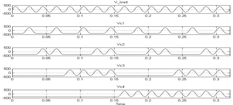
Fig.4 Voltage across capacitor (Vc1, Vc2, Vc3, Vc4).VI. SIMULATIONRESULTS
MATLAB/SIMULINK is used in this paper for simulation.
Data used in Simulation:-
Source
Voltage V = 400 V, Rs = 0.0287Ω, Ls = 0.20471mH. TBSC banks
Five TBSC banks are used in the simulation whose values are shown in Table I.
TABLE I:VALUES OF FIVE TBSC BANK
Sr. Q C L
No. (in KVAR) (in µF) (in mH)
1. 2.5 45 0.32
2. 5 90 0.16
3. 10 180 0.08
4. 20 360 0.04
5. 40 720 0.02
Continuously changing reactive power, QL is obtained by simulating three phase dynamic load. The nature of load variation is as
[image:6.612.102.509.478.666.2]Technology (IJRASET)
Fig.5 Simulation of three phase dynamic load.
Minimum reactive power Qmin, maximum reactive power Qmax, and base reactive power Qbase can be varied by changing the
parameters of three phase dynamic load. In all simulations QRef is set to zero since it is assumed that desired P.F.is unity at all times.
A. TBSC CLOSED LOOP OPERATION
Discrete PI controller with KP = 0.565 and KI = 25 is used. 5 bit ADC is used in simulation. Parameters of Three-phase dynamic load block are adjusted in such a way that QL varies continuously from QMin. = 1 KVAR to QMax. = 41 KVAR with base load QBase. = 10 KVAR. This variation takes place in five seconds. Waveforms of load reactive power QL, reactive power given by TBSC, Qcomp.(TBSC) and actual reactive power QActual at PCC are shown in Fig.6.
Fig.6 Simulation Result of TBSC operation.
Technology (IJRASET)
©IJRASET: All Rights are Reserved
414
VII.CONCLUSION
A topology using a TBSC has been presented. The TSC bank step values are chosen in binary sequence weights to make the resolution small. Current flowing through TBSC as well as source is transient free. Harmonic content in source current is negligibly small. By coordinating the control of TBSC, it is possible to obtain fully stepless control of reactive power. Also one can operate the system at any desired power factor. Proposed topology can compensate for rapid variation in reactive power on cycle to cycle basis. An attempt is made through this work to develop a scheme with thyristors to reduce the cost by avoiding IGBT‘s and IGCT‘s, technically sound with reliable performance during both steady state and transient conditions, suitable for rapidly changing / fluctuating loads such as arc furnaces, tractions loads, welding equipments etc., and self regulating operations are practically both transient and harmonics free. The scheme developed is most suitable for highly nonlinear, fluctuating and harmonic generating loads. It gives following benefits:
A. Maintaining the power factor at unity.
B. Minimum feeder current and loss reduction.
C. Improvement in distribution feeder efficiency.
D. Improvement in the voltage at load end.
E. Relief in maximum demand and effective utilization of transformer capacity.
F. Saving in monthly bill due to reduction in penalty on account of poor power factor, and reduction in maximum demand charges.
G. Conservation of energy takes place.
H. It is possible to get stepless control of Q closely matching with load requirements
I. The combination offers greater flexibility in control.
REFERENCES
[1] C. Maffrand, J. W. Dixon, and L. Morán, “Binary controlled, static VAR compensator, based on electronically switched capacitors,” in Proc. IEEE PESC’98, pp.1392–1396, 1998.
[2] Juan Dixon, Luis Morán, José Rodríguez, Ricardo Domke, “Reactive power compensation technologies, state of–the-art review”,Proc. IEEE, vol. 93, no. 12, pp.2144-2164, 2005.
[3] U. Gudaru and D. R. Patil, “An Innovative Transient Free Adaptive SVC in Stepless Mode of Control”, World Academy of Science Engineering and Technology 77 2011, pp.200-207.
[4] R. Sastry Vedam and Mulukutla S. Sarma, Power Quality - VAR compensation in power systems, CRC press, Taylor and Francis Group 2009, pp.19–20. [5] C.Sankaran, Power Quality, CRC press LLC, 2002. pp.12–24.
[6] L. Smith, “A practical approach in substation capacitor bank applications to calculating, limiting and reducing the effects of transient current,” IEEE Trans. Ind. Applicat., vol. 31, pp. 721–724, July/Aug. 1995.