Thesis by Abbas Komijani
In Partial Fulfillment of the Requirements For the Degree of
Doctor of Philosophy
CALIFORNIA INSTITUTE OF TECHNOLOGY
Pasadena, California 2006
© 2006
Abbas Komijani
Acknowledgement
I would like to express my deep and sincere gratitude to all who made this work possible. I am especially grateful to Professor Ali Hajimiri for his constant support and guidance throughout my Ph.D. studies. His broad vision, together with his remarkable knowledge of our field of research, has proved to be invaluable in defining my research direction. He has been a great instructor, supervisor, and friend.
I would like to thank my other committee members: Dr. Sander Weinreb, Professor David Rutledge, Professor Shuki Bruck, Professor Changhuei Yang, and Dr. Larry D'Addario for their assistance, helpful comments, and insightful suggestions.
I am also grateful to my colleagues: Arun Natarajan, Xiang Guan, Aydin Babakhani, Hossein Hashemi, Ehsan Afshari, Behnam Analui, James Buckwalter, Ichiro Aoki, Scott Kee, Donhee Ham, Hui Wu, Roberto Aparicio, Chris White, Yu-Jiu Wang, Hua Wang, Edward Keehr, Florian Bohr, and Sam Mandegaran. This work would not have been possible without their help.
I would also like to thank the Caltech staff: Michelle Chen, Naveed Near-Ansari, John Lilley, Niklas Wadefalk, Linda Dozsa, Jim Endrizzi, and Tess Legaspi, whose support has created a student-friendly environment.
This research has been supported by the Lee Center for Advanced Networking, the Office of Naval Research, the National Science Foundation, and trusted foundry program of DARPA.
I am thankful to my supportive friend, Payman Shanjani, who has always encouraged me to excel.
my brothers and sisters, who have always believed in me. Their unconditional love has been the greatest source of energy to me.
Abstract
Phased-array systems, a special case of multiple-input-multiple-output (MIMO) systems, take advantage of spatial directivity and array gain to increase spectral efficiency. Implementing a phased-array system at high frequency in a commercial silicon process technology presents several challenges. This thesis focuses on the architectural and circuit-level trade-offs involved in the design of the silicon-based fully integrated phased-array transmitters.
As the first implementation, a four-element 24GHz 0.18µm CMOS phased-array transmitter with integrated power amplifiers is presented. On-chip power amplifiers use substrate-shielded slow-wave transmission lines for impedance matching and can generate up to 14dBm of output power. The transmitter employs a two-step upconversion architecture with 4.8GHz as the intermediate frequency (IF) and uses a single 19.2GHz synthesizer serving as the local oscillator (LO) generator. The phased-array, employing the LO phase shifting architecture, achieves 23dB of peak to null-ratio when all four elements are used, demonstrates a beam steering range covering all signal incident angles, and can support a data rate of 500Mbps with a quadrature phase-shift keying (QPSK) baseband signal.
26GHz, is generated by dividing the VCO frequency by a factor of 2 using a cross-coupled injection-locked frequency divider. The on-chip 77GHz power amplifier with an output power of 17.5dBm and peak power added efficiency (PAE) of 14% achieves the best performance demonstrated in silicon. A single transmitter path achieves a 40dB conversion gain at 77GHz with 2.5GHz of bandwidth and a maximum output power of 12.5dBm.
Contents
Acknowledgements iii
Abstract v
List of Figures x
List of Tables xv
Chapter 1 Introduction... 1
1.1 Organization ...2
Chapter 2 Fundamentals of Multi-Path Transceivers... 4
2.1 A Historical Note ...5
2.2 High Frequency Circuit Design: Challenges and Opportunities...6
2.3 Phased-Array Principles...8
2.4 Phased-Arrays: A Special Case of Multiple-Input Multiple-Output (MIMO) Systems...13
2.5 Phased-Array Applications ...14
2.6 Phased-Array Architectures ...19
2.6.1 Time Delay vs. Phase Shift... 19
2.6.2 Implementation of the Phase Shift: Choice of Architecture... 21
2.6.3 Effects of Narrowband Approximation ... 24
2.6.4 Using OFDM to Remedy the Error Caused by the Constant Phase Shift Approximation... 28
2.7 Wireless Communication at Millimeter-Wave Frequencies ...30
2.8 Chapter Summary...33
Chapter 3 A 24GHz, +14.5dBm Fully-Integrated Power Amplifier in 0.18μm CMOS ... 35
3.2 Power Requirements in the 24GHz Band...37
3.3 Circuit Design ...38
3.3.1 Substrate-Shielded Coplanar Waveguide Structure... 38
3.3.2 Characterization of the Substrate-Shielded CPW Structure ... 41
3.3.3 Single-Transistor Power Gain and Stability ... 44
3.3.4 Stability of the Cascode Pair... 46
3.3.5 Amplifier Design ... 48
3.3.6 Low-Frequency Stability of the Amplifier ... 50
3.3.7 Wirebond and Pad Parasitic Effects ... 50
3.4 Experimental Results...51
3.5 Chapter Summary...57
Chapter 4 A Fully-Integrated 24GHz Phased-Array Transmitter in CMOS ... 58
4.1 Introduction ...58
4.2 Transmitter Architecture ...60
4.3 Power Amplifier and on-chip Balun ...65
4.4 Experimental Results...67
4.5 Chapter Summary...76
Chapter 5 A Wideband 77GHz, 17.5dBm Fully-Integrated Power Amplifier in Silicon... 77
5.1 Introduction ...77
5.2 The Required Amplifier Power for Automotive RADAR Application ...78
5.3 Conductor-Backed Coplanar Waveguide as the Transmission Line Structure .80 5.4 Amplifier Design...84
5.4.1 Circuit Schematic and Bias... 84
5.4.2 Design of the Matching Networks... 87
5.4.3 Output Stage Power Combining ... 89
5.4.4 Simulation and Layout Methodology ... 91
5.6 Chapter Summary...99
Chapter 6 A 77GHz Fully-Integrated Phased-Array Transceiver... 101
6.1 Introduction ...102
6.2 Local LO-Path Phase-Shifting Architecture...104
6.3 Transceiver Architecture ...107
6.4 Circuit Design ...111
6.4.1 52GHz Phase Rotator ... 111
6.4.2 Power Amplifier and On-Chip Image-Rejection Filter ... 115
6.4.3 IF and RF Stages... 116
6.4.4 52GHz Voltage-Controlled Oscillator... 118
6.5 Measurement Results ...119
6.6 Chapter Summary...128
Chapter 7 Conclusion ... 129
7.1 Recommendations for Future Work...130
List of Figures
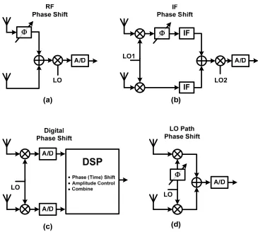
Figure 2.1 (a) array transmitter focuses the beam at a desired angle. (b) Phased-array receiver focuses on desired signal while it attenuates interferer coming from other direction. ... 9 Figure 2.2 Phased-array transmitter focusing the radiated power. ... 10 Figure 2.3 Phased-array receiver improves SNR and, rejects interferers. ... 11 Figure 2.4 Concept of a 21GHz satellite system using phased-array antenna to emit more power to areas with a larger path-loss due to rain [25]... 15 Figure 2.5 Automotive radar sensors providing multiple driving-aid functions... 17 Figure 2.6 Narrowband approximation of a delay with a constant phase shift... 20 Figure 2.7 Understanding the source of dispersion in a phased-array transmitter when a time delay is approximated with a constant phase shift. (a) Time delay in RF provides wideband beam forming. (b) Equivalent system by moving the delay before the mixer. (c)(d) Elimination of time delay in baseband results in dispersion. Note that only phase shift is required now, and it can be implemented in the LO, IF, or RF paths... 20 Figure 2.8 Different architectures for implementing phase shift. (a) RF phase shifting. (b) IF phase shifting. (c) Digital phase shifting. (d) LO-path phase shifting. ... 22 Figure 2.9 (a)(b) Simulated constellation spreading due to constant phase shift
approximation for an eight element phased-array transmitter (or receiver) employing a QPSK modulation for bandwidths 750MHz and 7.5GHz. Carrier frequency is 24GHz, and incidence angle is 90o. (c) EVM for the two constellations in parts (a) and (b) versus angle of incidence. (d) The effect of phase quantization error for 3-bit, 4-bit, and 5-bit resolution at different beam angles, as compared with a continuous LO phase-shift
resolution... 25 Figure 2.10 EVM improvement provided by normalized OFDM-QPSK modulation over ordinary QPSK modulation for an 8-elemt and 16-element receiver (or transmitter)... 29 Figure 2.11 Comparison of channel capacities for different system parameters
Figure 2.12 Channel capacity for different transmitter-receiver separations at 24GHz [53]... 33 Figure 3.1 A 4-path phased-array transmitter for a 24GHz point-to-point wireless
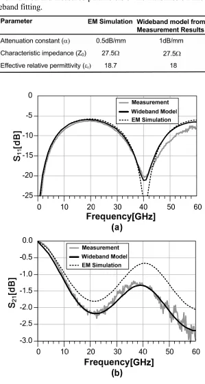
connection... 37 Figure 3.2 Combination of (a) CPW and (b) Microstrip structures to realize (c) substrate-shielded CPW structure... 39 Figure 3.3 Electric and Magnetic field distributions from 3D EM simulations of (a), (b) a normal CPW structure, and (c), (d) a substrate-shielded CPW structure. ... 41 Figure 3.4 Die photo of the substrate-shielded CPW test structure; shield layer consists of 4μm-wide stripes with 2μm spacing. ... 42 Figure 3.5 Simulated and measured S-parameters of the transmission line. (a) Reflection parameter (S11) and (b) Transmission parameter (S21)... 43
Figure 3.6 Unilateral model of MOS transistor with conjugate-matched source and load terminations is used to calculate the maximum unilateral power gain. ... 45 Figure 3.7 Model of MOS amplifier used to derive stability criterion. ... 46 Figure 3.8 (a) Self-bias of cascode transistor pair. (b) Equivalent circuit for the analysis of stability. ... 47 Figure 3.9 Schematic of the 24GHz, 14.5dBm fully-integrated CMOS power amplifier. ... 49 Figure 3.10 Design of the output matching network; the smith chart reference impedance is the characteristic impedance of the transmission lines (27.5Ω)... 50 Figure 3.11 Die micrograph of the amplifier; chip size: 0.7mm x 1.8mm... 52 Figure 3.12 Large-signal measurement setup. ... 52 Figure 3.13 Output power and amplifier gain vs. available input power using a 2.8V supply... 54 Figure 3.14 Two-tone measurement of the amplifier; the two tones are applied at
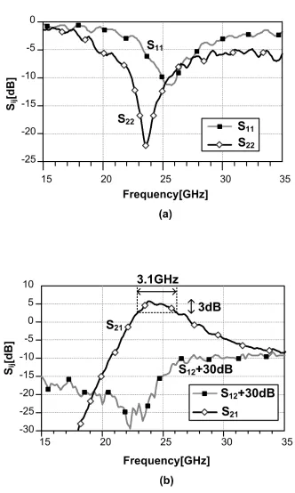
23.9GHz and 24GHz... 54 Figure 3.15 Measured S-parameters of the amplifier; VG1= VG3=1V, VDD=2.8V, and
Isupply=100mA. (a) Reflection parameters. (b) Transmission parameters. ... 56
Figure 4.3 Architecture of the single transmitter element and transmitter frequency plan.
... 65
Figure 4.4 Balun for differential to single-ended conversion at PA input... 66
Figure 4.5 Two-stage on-chip power amplifier. ... 67
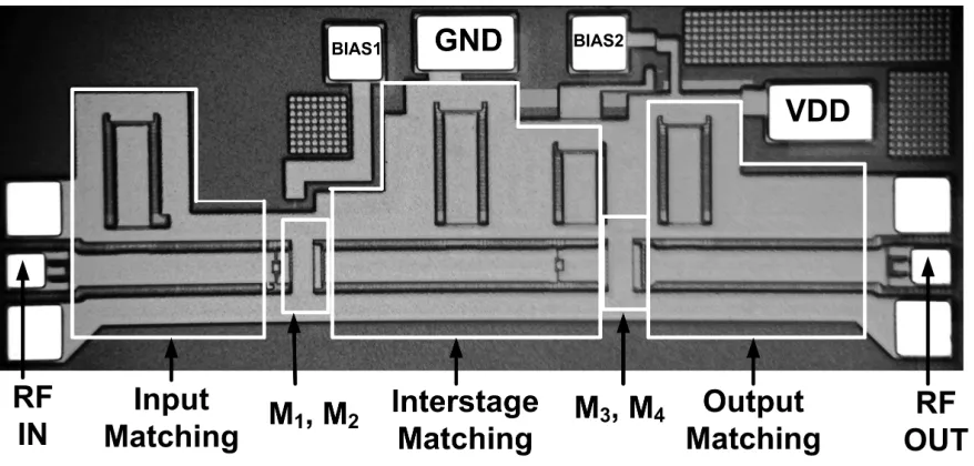
Figure 4.6 Die micrograph of 24GHz 4-element phased-array transmitter. ... 68
Figure 4.7 Measurement setup to characterize transmitter performance. ... 69
Figure 4.8 PA output matching with probe-based testing and wirebonds to PCB... 70
Figure 4.9 Phased-array measurement setup... 72
Figure 4.10 Comparison of theoretical and measured array pattern with two and four elements active... 73
Figure 4.11 Output spectrum of transmitter for 100- and 500-Mbps QPSK input. (a) Output spectrum for 100-Mbps QPSK input. (b) Output spectrum for 500-Mbps QPSK input. ... 74
Figure 5.1 (a) Typical range and resolution for a long-range car radar. (b) The required main beam width to be able to resolve two cars in two adjacent lanes. (c) Calculation of the directivity of the transceiver. ... 80
Figure 5.2 (a) Conductor-backed coplanar waveguide transmission line structure used for matching in the amplifier. (b) The simulated magnetic field distribution of the structure, showing most of the return current coming from the side shields... 82
Figure 5.3 The simulated isolation between two side-by-side 400μm, 50Ω microstrip lines with sideshield (W = 5μm, S = 7.5μm) and without sideshield (W = 13μm)... 83
Figure 5.4 Schematic of the 77GHz power amplifier including element values. ... 84
Figure 5.5 Transistor in the open base and open emitter configurations. ... 85
Figure 5.6fT versus breakdown voltage relationship of SiGe HBTs [102]. ... 86
Figure 5.7 Load-pull simulation of the four stages of the power amplifier, together with the actual realized load impedances... 88
Figure 5.8 Lowering sensitivity to matching errors in the output stage: load-pull result of the output stage plotted for different reference characteristic impedances in the matching network. ... 89
Figure 5.10 Die micrograph of the 77GHz power amplifier, chip size: 1.35x0.45mm2.. 92
Figure 5.11 Layout of one of the output parallel branches consisting of two transistors (depicted as Q5 in the amplifier schematic and layout). ... 93
Figure 5.12 Waveguide-based large-signal measurement setup used for the large signal characterization of the PA... 94
Figure 5.13 Small-signal gain (S21) of the amplifier simulated and measured between 65GHz and 100GHz... 95
Figure 5.14 Frequency variation of the output power of the BWO. ... 95
Figure 5.15 Measured large-signal parameters of the amplifier at 77GHz... 97
Figure 5.16 Measured saturated power and PAE for a supply range of 1-2.5V. ... 97
Figure 5.17 Measured saturated power, gain, and PAE versus frequency... 98
Figure 6.1 (a) Centralized LO-path phase shifting approach. (b) Earlier implementations of the centralized multiple phase generation approach... 105
Figure 6.2 Local LO-path phase shifting architecture. ... 106
Figure 6.3 Simulated phase noise of the 50GHz synthesizer... 107
Figure 6.4 Architecture of the fully-integrated 77GHz phased-array transceiver. ... 109
Figure 6.5 (a) Schematic of the 52GHz phase rotator in each element. (b) Use of interpolation to generate phase shift. (c) Simulated amplitude variation of phase rotator. (d) Layout of the phase rotator... 113
Figure 6.6 (a) Distribution of the possible phase shifts due to limited DAC resolution (plotted in one quadrant). (b) RMS phase shift error versus DAC resolution. (c) Maximum phase shift quantization error. ... 114
Figure 6.7 (a) The schematic of the transmitter IF filter. (b) Layout of the filter test structure. (c) Simulated and measured reflection coefficient (S11) and (d) transmission coefficient (S21) of the filter test structure... 116
Figure 6.8 IF Stage... 117
Figure 6.9 RF Stage. ... 118
Figure 6.10 52GHz voltage-controlled oscillator. ... 119
Figure 6.11 Die micrograph of the 4-element 77GHz phased-array transceiver. ... 121
Figure 6.12 Transmitter single-element measurement setup. ... 122
List of Tables
Table 2.1 Gain loss due to phase shifter quantization... 28
Table 3.1 Simulated and measured parameters of the transmission line at 24GHz with wideband fitting. ... 43
Table 3.2 Measured performance summary of the power amplifier ... 55
Table 4.1 Transmitter Performance Summary ... 75
Table 5.1Amplifier Performance Summary... 98
Table 5.2Comparison between this work and previously reported integrated high-frequency PAs... 100
Chapter 1
Introduction
Introduction
Today, silicon and specially RF CMOS are the dominating force in most commercial wireless applications. Cellular radio, wireless local area networks (WLAN), global positioning system (GPS), and Bluetooth are just examples of the silicon-centric paradigm in wireless communications [1]. The transition from III-V based technologies (that were accompanied by bipolar and BiCMOS ones) to a CMOS-dominated mindset has taken less than a decade. This seemingly ubiquitous adoption of silicon, and particularly CMOS, is no accident. It stems from the reliable nature of silicon process technologies that make it possible to integrate millions of transistors on a single chip with extraordinary yields, combined with the digital-friendly nature of the CMOS processes.
Silicon offers a new set of possibilities and challenges for RF and microwave applications. While the high cut off frequencies of the SiGe heterojunction bipolar transistors (HBTs) and the seemingly perpetual shrinking feature sizes of the MOSFETs hold a lot of promise [2], new design techniques needs to be devised to deal with the realities of these technologies, such as low breakdown voltages, lossy substrates, large interconnect parasitics, and high frequency coupling issues. To deal with the limitations and opportunities of this new paradigm in high-speed and microwave design, it seems almost inevitable that new design methodologies that take advantage of multiple-signal paths and distributed approaches will have to be applied more often. One example of such multiple signal path approaches is phased-array systems.
efficiency. Integration of high-frequency phased-array systems in silicon (e.g., CMOS) promises a future of low-cost radar and gigabit-per-second wireless communication networks. In communication applications, phased-array provides an improved SNR via formation of a beam and reduced interference generation for other users. The practically unlimited number of active and passive devices available on a silicon chip and their extremely tight control and excellent repeatability enable new architectures that are not practical in compound semiconductor module-based approaches.
The objective of this work is to investigate the possibility and find new techniques to overcome the difficulties encountered in integration of theses systems at millimeter-wave frequencies in silicon-based processes.
1.1 Organization
After reviewing multiple-path radio transceiver fundamentals, the basic operation of phased-arrays will be discussed in Chapter 2. Then, the advantages, architectures, and applications of phased-arrays will be discussed in detail.
Chapters 3 and 4 will present the first step of implementing these systems in silicon. A 24-GHz 0.18µm CMOS phased-array transmitter with integrated power amplifiers is presented. On-chip power amplifiers use substrate-shielded slow-wave transmission lines for impedance matching and can generate up to 14dBm of output power. The transmitter employs a two-step upconversion architecture with 4.8GHz as the IF frequency and uses a single 19.2GHz synthesizer serving as the LO generator. The phased-array, employing the LO phase shifting architecture, achieves 23dB of peak to null ratio when all four elements are used, demonstrates a beam steering range covering all signal incident angles, and can support a data rate of 1Gb/s with a QPSK baseband signal.
52GHz is generated by the VCO and distributed to all RF paths. The phase shifting is performed at the LO ports of the RF mixers with continuous analog phase shifters. The quadrature signal of the second LO is generated by dividing the VCO frequency by a factor of 2 using a cross-coupled injection-locked frequency divider. The on-chip 77GHz power amplifier with an output power of 17.5dBm and peak power added efficiency (PAE) of 14% achieves the best performance demonstrated in silicon. A single transmitter path achieves a 40dB conversion gain at 77GHz with 2.5GHz of bandwidth and a maximum output power of 12.5dBm.
Chapter 2
Fundamentals of Multi-Path TransceiversFundamentals of Multi-Path Transceivers
It is becoming increasingly difficult to achieve further improvements in spectral efficiency using purely time and frequency domain methods. Interestingly, there are spatial methods that can be used to improve data rates without the dreaded increase in bandwidth. Therefore, exploiting the spatial dimension for improving spectral efficiency is an area of rapidly increasing interest. Multiple antenna systems have been identified as one means of effectively increasing the spectral efficiency by taking advantage of spatial directivity and diversity as well as array gain via the multi-path scattering that is present in most indoor and urban environments. The antenna size and the spacing between the elements are inversely proportional to the frequency. This inspires a move to higher frequencies to leverage spatial processing techniques, as multiple antenna systems can be made physically smaller. In addition, larger bandwidths are available at higher frequencies. Small-sized, highly-integrated, low-power multiple antenna systems can also be used for ranging and sensing applications, i.e., radar.
2.1 A Historical Note
Gordon Moore’s seminal paper published in 1965 [2] starts with the following prediction:
“The future of integrated electronics is the future of electronics itself. The advantages of integration will bring about a proliferation of electronics, pushing this science into many new areas.
Integrated circuits will lead to such wonders as home computers - or at least terminals connected to a central computer - automatic controls for automobiles, and personal portable communications equipment. The electronic wristwatch needs only a display to be feasible today.
But the biggest potential lies in the production of large systems. In telephone communications, integrated circuits in digital filters will separate channels on multiplex equipment. Integrated circuits will also switch telephone circuits and perform data processing.
Computers will be more powerful, and will be organized in completely different ways. For example, memories built of integrated electronics may be distributed throughout the machine instead of being concentrated in a central unit. In addition, the improved reliability made possible by integrated circuits will allow the construction of larger processing units. Machines similar to those in existence today will be built at lower costs and with faster turn-around.”
continue to provide us with an ever-increasing number of transistors that in many cases render human creativity the primary bottleneck to further advancements.
In the last paragraph of Gordon Moore’s 1965 paper, he also predicted that:
“Even in the microwave area, structures included in the definition of integrated electronics will become increasingly important. … The successful realization of such items as phased-array antennas, for example, using a multiplicity of integrated microwave power sources, could completely revolutionize radar.”
Integration of a complete phased-array system in silicon results in substantial improvements in cost, size, and reliability. At the same time, it provides numerous opportunities to perform on-chip signal processing and conditioning without having to go off-chip, leading to additional savings in cost and power. The multiple signal paths operating in harmony on both the transmitter and receiver side provide benefits at the system and circuit level. The use of such phased-arrays is not restricted to traditional areas such as radar alone. For example, high frequency integrated phased-array-based systems will make gigabit-per-second directional point-to-point communication networks feasible. At the circuit level, the division of the signal into multiple parallel paths relaxes the signal handling requirements of individual transistors.
In this thesis, two complete phased-array systems are presented which demonstrate the first successful implementation of an entire microwave system in silicon. The first one is a fully-integrated CMOS-based 4-element phased-array transmitter with on-chip power amplifiers [8][9], and the second one a 0.12μm SiGe 4-element phased-array transceiver with integrated dipole antennas [10][11][12]. Such phased-array systems can be used for high speed directional communications as well as ranging and sensing applications such as radar. These silicon-based phased-array systems realize Moore’s last prediction almost 40 years later.
2.2 High Frequency Circuit Design: Challenges and Opportunities
by scaling transistors’ physical dimensions, thereby lowering the charge transit time and junction parasitic capacitances, which in turn results in an increase in the maximum usable frequency. Improved lithography techniques in conjunction with advancements in ion implantation and rapid thermal cycles have made it possible to define smaller lateral and vertical dimensions.
Shrinking the physical dimensions of the transistors must be accompanied by a proportional reduction in the width of the depletion regions inside the transistor to maintain its basic operation. This is achieved by an overall increase in the doping concentrations of the transistor. Unfortunately, the higher doping levels increase the electric field inside the transistor, reducing its breakdown voltages, thereby necessitating lower voltage swings and supply voltages [13][14]. Also, higher doping levels in the substrate result in lower substrate resistivity. The higher substrate conductivity of silicon-based processes introduces additional inductive energy loss mechanisms in passive components, such as inductor and transmission lines, that are extensively used in high-speed, radio frequency (RF), and microwave integrated circuits.
While lower breakdown voltages and low quality passive components may not be a major impediment for the core of digital processors and memory units, they pose major challenges for high-speed I/O as well as RF and microwave integrated circuits. Incidentally, there has been tremendous growth in these areas in the recent years fueled by the prospects of wide-scale integration of analog, RF, and digital circuitry on the same substrate to eliminate the overhead of interface circuitry and lower the cost.
In MOSFETS, smaller dimensions result in shorter transit times and lower parasitic capacitances. Even in a velocity-saturated MOSFET, a reduction in the channel length improves the cutoff frequency by lowering the gate-source capacitance. This improvement will be eventually limited by the drain and source junction capacitors which scale sublinearly. This scaling also reduces breakdown voltages.
transistors, one way to do this is by lowering the bandgap energy of the base region, by introducing Germanium atoms in the base of a standard silicon bipolar junction transistor (BJT), thereby creating a hetero-junction bipolar transistor (HBT). The lower bandgap in the base region increases the height of the potential barrier for the holes being injected back into the emitter (in an NPN transistor) improving the emitter injection efficiency, γ, of the transistor. The resulting higher emitter injection efficiency makes it possible to increase the doping level in the base region, lowering the physical base resistance. Additionally, the non-uniform doping profile in the base can be engineered to facilitate the charge diffusion from the emitter to the collector, thus reducing the base transit time. A higher base doping level results in a larger Early voltage, VA, for the transistor and/or a
reduction in the collector series resistance achieved by increasing the collector doping concentration. These modifications have made it possible to fabricate SiGe transistors with cut-off frequencies in excess of two hundred gigahertz [15]-[17].
The practically unlimited number of high frequency transistors with limited voltage and power handling capabilities necessitate a fresh look at the way we design circuits. System and circuit designers are just beginning to recognize the plethora of new possibilities that this new paradigm offers.
To deal with the limitations and opportunities of this new paradigm, it is necessary to adopt a design approach that allows for more integral co-design at the system, circuit, and device level. In high-speed and microwave design, it seems almost inevitable that new design methodologies that take advantage of multiple-signal paths and distributed approaches will have to be applied more often [18]. One example of such multiple signal path approaches is phased-array systems.
2.3 Phased-Array Principles
A phased-array transmitter or receiver consists of several signal paths, each connected to a separate antenna. The antenna elements of the array can be arranged in different spatial configurations [7]. The array can be formed in one, two, or even three dimensions, with one, or two-dimensional arrays being more common.
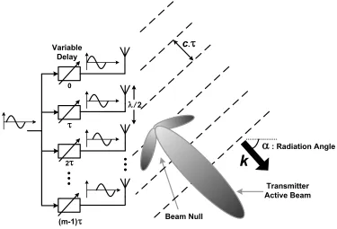
[image:24.612.118.529.73.293.2]The principle of operation of a phased-array is similar for a receiver or a transmitter. Figure 2.2 shows a simplified n-element phased-array transmitter. When the input signal,
s(t), is distributed to elements that delay the signal by multiples of τ, the combined signal in a direction, θ, is given by
( )
1(
)
0 sin 1 n k d S t s t k n k
c θ τ − = ⎛ ⎞ = ⎜ − − − − ⎟ ⎝ ⎠
∑
. (2.1)Therefore, the signals from all elements add up coherently in the direction, sin 1 c.
d
τ
θ = − ⎛ ⎞
⎜ ⎟
⎝ ⎠, where d is the spacing between antennas and c is the velocity of light. This coherent addition increases the power radiated in the desired direction,
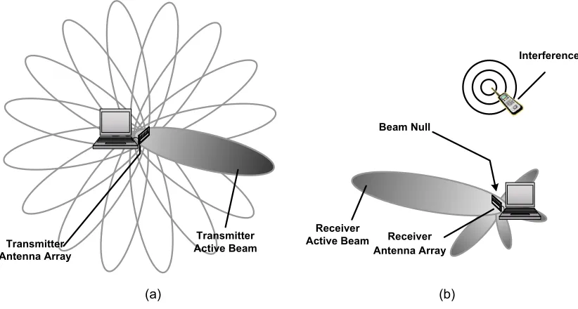
(a) (b) Antenna Array Transmitter Beam Null Receiver Antenna Array Transmitter Active Beam Receiver Active Beam Interference
while incoherent addition of the signal in other directions ensures lower interference power at receivers that are not targeted. It can be seen from (2.1) that in an m-element transmitter, if each element radiates P watts omni directionally, the Effective Isotropic Radiated Power (EIRP)1 in the main beam direction is m2P watts. For example, if each transmitter in a four-element array radiates 14dBm, the EIRP in the beam direction is increased by 12dB (20log104) to 26dBm. This increase in signal power at the receiver is
particularly useful at high frequencies, where the efficiency and output power of silicon-based power amplifiers is low, path-loss is high, and receiver sensitivity is low.
The benefits provided by the beam directionality of a phased-array transmitter can be likened to the advantages of a narrow flashlight beam over the omni-directional incandescent bulb. In a flashlight, most of the light energy is focused only in the desired direction, as opposed to a bulb’s indiscriminate illumination in all directions. Thus, to obtain a given power intensity at the destination, much lower power needs to be radiated
1 The EIRP in a particular direction is the power that an isotropic transmitter would have to radiate to cause
the same field strength in that direction.
Variable Delay
k
c.
Beam Null
Transmitter Active Beam
(m-1)
2 0
/2
[image:25.612.136.511.371.626.2]: Radiation Angle
at the source for a directional beam, as compared to an omni-directional one. At the same time, less interference is generated via this collimation of power.
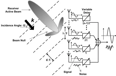
In a phased-array receiver, the radiated signal arrives at different times at each of the spatially separated antennas. The difference in the time of arrival of the signal at different antennas depends upon the angle of incidence and the spacing between the antennas. As shown in Figure 2.3, an ideal phased-array receiver compensates for the time delay difference between the signals from different antennas and combines the signals coherently to enhance the reception from the desired direction(s), while rejecting emissions from other directions.
Thus, in a phased-array based system, the transmitter generates less interference at receivers that are not targeted, and the receiver is also capable of nulling out interferers as long as they do not originate from the same direction as the signal. Additionally, for a given power level at the receiver, the power that has to be generated is lower in a phased-array transmitter than in an isotropic transmitter.
Variable Delay
k
c. Beam Null
Receiver Active Beam
(n-1)
2
0
/2 Incidence Angle:
Signal
[image:26.612.130.513.408.658.2]Noise
The advantage of phased-array receivers is not limited to nulling out interferers. A phased-array approach also provides better sensitivity at the receiver. For a given receiver sensitivity, the output signal-to-noise-ratio (SNR) sets an upper limit on the noise figure of the receiver. The noise figure, NF, is defined as the ratio of the total output noise power to the output noise power caused only by the source [19]. Consider the n-path phased-array receiver, shown in Figure 2.3. Since the input signals add coherently, the combined output is given by
Sout= n2G1G2Sin , (2.2)
where n is number of elements, and G1 and G2 correspond to the gains before and after
signal combining. The antenna’s noise temperature is primarily determined by the temperature of the object(s) it is pointed at. With sufficient antenna spacing, the black-body radiation noise of each antenna is uncorrelated to the noise of the other antennas in the array. References [20] and [21] investigate the validity of this assumption and also the effect of back-radiation of each receiver input noise to the other receivers through antenna coupling, which makes their noises partially correlated. Furthermore, the receiver noise sources in each signal path before power combining are independent.
Assuming that the antenna noise contributions in different elements are uncorrelated, the output total noise power is given by
Nout=n(Nin+N1)G1G2+N2G2 , (2.3)
where N1 and N2 are the input-referred noise contributions of the stages corresponding to gains G1 and G2, and Nin is the noise at the input of each antenna.
If a single receiver chain is used instead, the output signal would be
Sout= G1G2Sin (2.4)
and the noise power at the output of receiver will be
Thus, compared to the output SNR of a single-path receiver, the output SNR of the array is improved by a factor between n and n2 depending on the noise and gain contribution of different stages.
For a given NF, an n-element receiver can improve the sensitivity by 10log10(n) in dB compared to a single-path receiver. For instance, if the noise from the antennas is uncorrelated, an 8-path phased-array can improve the receiver sensitivity by 9dB. In other words, the time-delayed signals from the antenna array add in amplitude (coherently), while the noise adds in power (incoherently). This results in a 10log10(n) [dB] improvement in the SNR at the output of the n element phased-array receiver.
Thus, in a system based on phased-arrays at the transmitter and receiver, the higher SNR and lower interference increases channel capacity. Furthermore, the directivity of the phased-array transmitter-receiver system permits higher frequency reuse due to better interference suppression and rejection, leading to increased network capacity.
2.4 Phased-Arrays: A Special Case of Multiple-Input Multiple-Output
(MIMO) Systems
The antenna arrays can be implemented on either the transmit side (Multiple-Input Single-Output: MISO), the receive side (Single-Input Multiple-Output: SIMO), or on both ends (Multiple-Input Multiple-Output: MIMO).
capacity is possible (20-40 bit/s/Hz for an 8 transmitter-12 receiver MIMO system [24]). However, the spacing between the antennas has proven to be a practical barrier to the implementation of multiple antenna arrays for mobile applications at frequencies in the low GHz range (e.g., λ ~ 15cm @ 2GHz). The size constraints mandate the move to higher frequencies.
Phased-arrays, historically employed in radar and radio astronomy applications, are a class of multiple antenna systems. As discussed in Section 2.3, they can form beams and nulls in desired directions by controlling the time delay and gain of the signal in each path independently, while improving the sensitivity of the receiver. The array gain and spatial directivity achieved in a phased-array system provide a logarithmic increase in channel capacity with increase in the number of elements in the phased-array due to the logarithmic dependence of channel capacity on SNR.
The improvement in the SNR at the target phased-array receiver and reduction in the level of interference generated for the other users because of the directionality of a phased-array transmitter leads to a substantially higher data rates and frequency reuse ratios, while lowering the power requirements of the transmitter. Although there are more active elements in a phased-array system, its power consumption is still lower than that of single-path systems for the same data rate.
2.5 Phased-Array Applications
The phased-array concept has been widely used in radar systems which emit continuous-wave or pulse signals at certain directions and obtain the information of distant objects by analyses of the reflected waves. Radar is a fundamental apparatus for surveillance, object tracking, remote sensing, projectile guidance, and synthetic imaging. The electronic scanning of the beam of phased-array radar is orders of magnitude faster than the traditional radar rotated by mechanical motors.
[25], a phased-array approach is proposed to overcome the effect of rain attenuation, which is larger in 21GHz compared to lower satellite bands. As shown in Figure 2.4, concentrated radiation beams created by a phased-array antenna cover areas of heavy rain, and the same antenna covers other areas with a spread radiation beam. The adaptive beamforming also enables satellite programs to be delivered to mobile objects such as planes and vehicles [26].
Phased-arrays are used by many AM broadcast stations to enhance signal coverage in the city of license while minimizing interference to other areas [27]. Due to the differences between daytime and nighttime ionospheric propagation at AM broadcast frequencies, it is common for AM broadcast stations to change between day and night radiation patterns by switching the phase and power levels supplied to the individual antenna elements daily at sunrise and sunset.
The phased-array concept is used in optical communication for wavelength selective splitters. By programming the steering angle of an optical signal, a dynamic focus/defocus capability can be realized which enables a thin and flat lens. This area is currently an active area of research to enhance the quality of cell phone cameras. The necessary beam steering can be realized by moving two arrays of microlens with respect
to each other. Alternatively, the phase shifting can be done through patterning of an electrical addressing network on the substrate of a liquid crystal waveplate [28]. Refractive index changes large enough to realize full-wave phase shifts can be created using low (<10V) voltage applied to the liquid crystal phase plate electrodes.
Vehicular radar has been developed for decades and is being installed on high-end luxury sedans at the moment [31][32]. As shown in Figure 2.5, radar sensors mounted around the car can provide multiple driving-aid functions such as automatic cruise control (ACC), parking aid, blind spot detection, and side collision warning [33]. High resolution radar systems with advanced image processing and powerful signal processors can further enable object classification, roadside detection, and prediction of the lane course, thus making intelligent interpretation of traffic scenes imaginable [34]. Ultimately, autonomous driving is possible by combining short-range radar, global positioning techniques, and wireless communications. Radar appears to be the best sensor principle, because alternatives like video, laser, and ultrasound may have difficulties under bad weather conditions, when they are needed most. Additionally, radar offers the vehicle manufacturers a stylistic advantage of mounting behind a plastic bumper that can be considered nearly transparent to the radar signal without requiring specific cut-outs or similar accommodations.
Phased-arrays can provide the narrow beam and low sidelobe requirements of the automotive radar together with compact or even conformal antennas which are invisible to consumers having aesthetic judgments. Developing phased-arrays operating at 24GHz or 77GHz frequency bands allocated by Federal Communications Commission (FCC) for
Object Detection And Parking Aid
Blind Spot Side Impact
Pre-Crash Detection Adaptive
Cruise Control (77GHz)
Stop & Go
vehicular radar applications is an intense research topic at the moment [31]-[40].
Radio astronomy is another important application area of phased-array. The next generation radio telescope demands sensitivity one or two orders of magnitude higher than current telescopes in use, requiring a total collecting aperture of approximately one square kilometer [41]. Instead of using an ultra-giant single parabolic antenna, such a system can be implemented with an array of more than one-hundred million small antenna elements, providing additional benefits such as adaptive radio-interferences rejection and multiple simultaneous beam formation.
Biomedication is an emerging yet promising application of phased-array. In [42], a microwave imaging method is proposed using a phased-array to detect early-stage breast cancer. The antenna array placed at the breast surface emits the wideband impulses sequentially by each antenna. The beam-forming is employed at the receiver to focus the backscattered signal from the malignant tumor and compensate for the frequency-dependent propagation effect. The signal reflection is primarily due to the dielectric discontinuity at the edge of the malignant tumors and the normal breast tissue. The relevant contrast is an order of magnitude higher for microwave than for X-ray or ultrasound [43], suggesting a much higher detection probability. Microwave imaging is also a much cheaper solution than other current alternatives such as magnetic resonance imaging (MRI) and is less harmful to the patients than X-ray. In [44], a hyperthermia system is presented using a conformal phased-array to treat tumors in human limbs. The array consists of 8 dipole radiators mounted on a cylindrical surface, focusing EM waves to the tumor inside the limb to heat it to a higher temperature than surrounding tissues. The thermal pattern can be varied by adjusting the amplitude and phase of each antenna element. Tumors heated repeatedly to higher temperatures sometimes exhibit regression and necrosis.
In summary, phased-array provides us with various ways to explore the space dimension and take advantage of space diversity conveniently using electronic methods. Its potential application range is only limited by the imagination of the engineers.
2.6 Phased-Array Architectures
2.6.1 Time Delay vs. Phase Shift
Phased-array is perhaps a misnomer for these systems given that true time delay, and not phase shift, is required in each path for coherent addition of signals. As shown in Figure 2.3, when a plane electromagnetic wave arrives at an antenna array at an angle of α with respect to the normal to the array plane, the signal is received by each antenna at a different time due to the difference in propagation path length. In general, an angle-dependent time delay in each path at the receiver can compensate for the arrival delay and effectively “listen” to a desired direction. In a one-dimensional array, the angle of incidence, α, is related to the delay difference of two adjacent elements, τ, the spacing of two adjacent antennas, D, and the speed of light, c, via
τ
α
) .sin(
. c
D = (2.6)
the choice of where to implement the phase shift doesn’t matter, the choice of where to implement the phase shift has significant architectural implications and will be addressed in the following section.
[image:35.612.163.486.328.612.2]Delay [Time] Phase
Figure 2.6 Narrowband approximation of a delay with a constant phase shift.
2.6.2 Implementation of the Phase Shift: Choice of Architecture
Advances in silicon process technologies for integrated circuits have resulted in very fast transistors with cut-off (unity current gain) frequencies above 200GHz. However, transistor speed is only one of the parameters affecting the system operation. Additional constraints imposed by the low breakdown voltages, losses of integrated passive elements, low power budget, as well as cost and area constraints have important bearing on the overall system performance. Therefore, the architecture of the phased-array system has to be chosen carefully to ensure repeatability and reliability.
Ideally, broadband variable delays are needed to make the signals from all the paths coherent before they are combined. Such a variable delay, if implemented in the signal path at RF, can reduce power consumption. The gain of the delay stage should be independent of the delay, as a change in amplitude with different delays will lead to distortion when the signals are combined. Thus, the delay element should have large and accurate variations in delay (0 to 140ps @ 24 GHz for an 8-element array, with spacing of λ/2 between antennas) and low loss. However, implementing a broadband, low-loss, true-time delay element at RF which is capable of large variation, occupies practical area, and scales well with an increase in number of elements poses several problems.
An architecture with controllable phase-shifters in each RF path and signal combining at RF has advantages with respect to lower power consumption, as there only needs to be one IF/baseband stage (Figure 2.8(a)). Additionally, since all the interferers are nulled out at RF, the linearity requirements of the IF/baseband stage are reduced. If the signal is delayed by time, τ, the carrier at frequency, fc , undergoes a phase shift equal to 2πfcτ.
[image:37.612.137.502.70.398.2]Since a phase shift of Φ is equivalent to a phase shift of 2π + Φ, the phase shifter only needs to provide phase shifts between 0 and 2π. Again, the gain should be constant across phase shifts, and the phase-shifter should have low loss. There have been some phase shifters reported at lower frequencies, but their size and performance do not make them suitable for an integrated phased-array system. The study of high frequency phase shifters is an active area of research [4][47]-[48]. If the phase-shifter loss is not uniform for all
phase shifts, variable gain amplifiers are required in each element to equalize the phase-shifter losses to avoid array pattern degradation.
While it is possible to utilize phase-shifters in the IF stage, they increase power consumption because in an n element receiver, there will have to be n down-conversion mixers before the phase shifters (Figure 2.8(b)). Since the value and, therefore, the size of passive components (i.e., inductors, capacitors, and transmission lines) needed to provide phase shift is inversely proportional to the frequency, implementing the phase shifters at IF will increase system area.
Another architectural choice is to avoid analog phase-shifting entirely, opting for baseband digital delay (Figure 2.8(c)). This increases the flexibility of the system, as it can now be configured both as a phased-array or a MIMO system depending on the application. However, this advantage is offset by the high power consumption of such a system, which is essentially equivalent to n receivers operating in parallel while sharing no blocks except the frequency synthesizer. Additionally, as the interferers are still present, the linearity and dynamic range of the IF stage and the A/D converter will also have to be substantially higher, leading to higher power consumption. As an illustration, imagine a digital array of 8 receivers where each has a 8 bit analog-to-digital converter that samples the signal with a 100MHz channel bandwidth at twice the Nyquist rate. These numbers are reasonable for such a system. The baseband data-rate of the whole system can be calculated as 76.8Gb/s. This requires a high speed interface and a power hungry and expensive signal processing core.
only one IF amplifier followed by two (I and Q) A/D converters the power consumption is reduced as compared to an IF phase shift architecture.
2.6.3 Effects of Narrowband Approximation
As discussed in Section 2.6.1, the narrowband phase-shift approximation leads to some signal distortion due to dispersion. The input signal that is distributed to each element in a phased-array transmitter (or receiver) can be represented as s t
( )
=v t( )
cos⎣⎡ωRFt+φ( )
t ⎤⎦, where v t( )
and φ( )
t represent the baseband signal modulating the carrier. When phase shifts are implemented in each element to achieve a radiation angle of θ for which the propagation delay between successive elements differs by τ, the combined signal power is( )
1(
)
(
)
0
.cos
n
RF k
S t − v t kτ ω t φ t kτ
=
=
∑
− ⎡⎣ + − ⎤⎦. (2.7)Thus, none of the phase-shifting architectures ensure that the baseband modulating signals add up coherently, resulting in signal distortion. The signal degradation is independent of the mechanism and/or the architecture used to produce the phase shift (RF phase shift, LO phase shift, or IF/Baseband phase shift). The phase shifting approach makes the carrier phase at different paths coherent, but due to the constant phase shift and, hence, zero group delay, it does not synchronize the baseband modulation signals.
When the ratio of modulation bandwidth to carrier frequency increases, the signal dispersion increases, manifested by the spreading of the constellation points. This distortion results in a higher error vector magnitude (EVM) and results in an increased bit error rate (BER) in wireless communication systems and in a reduced radial resolution in radar applications. The EVM increases with an increase in the number of elements and/or the bandwidth of the baseband signal and can be a source of error on both the transmitter and the receiver side, leading to higher bit-error rates [50].
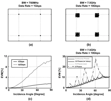
constellation of the received signal (without noise) for an 8-element phased-array receiver at bit rates of 1Gbps and 10Gbps at the worst-case incident angle of 90o with respect to normal, using a QPSK binary-coded complex modulation scheme at a carrier frequency of 24GHz. The antenna elements are placed λ/2 = 6.25 mm apart in a one dimensional array of eight elements. Receiver noise was not simulated to fully expose the limitations of the constant phase approximation. A square-root raised cosine filter with a roll-off factor (β) of 0.5 is used at both transmitter and receiver for pulse shaping. A β of 0.5 corresponds to a spectral-efficiency of 1.33 bits/s/Hz [51].
As the direction of the beam becomes more oblique, the delay between the paths increases and so does the error introduced by constant phase-shift approximation. The constellation spreading is a function of the incidence angle of the signal, ratio of signal-bandwidth to carrier-frequency, and the pulse shaping used. Error vector magnitude (EVM) is a measure of constellation spreading and is the root mean squared difference between the perfectly demodulated signal and the distorted signal. The EVM of the received signal was calculated for different signal bandwidths and angles of incidence, and the results are plotted in Figure 2.9(c). This was done for a continuous phase control at the LO. As can be seen, for a carrier of 24GHz, even for bit rates as high as 1Gbps and an incidence angle of 90o (worst case), EVM is lower than 2%, and so the signal integrity is maintained without additional equalization. Given the 250 MHz wireless communication bandwidth, phase-shift of the carrier at 24 GHz (a BW/fcenter close to a
factor of 0.01) is a very good approximation for the delay and is sufficient for reliable communication. However, for broadband communication or to achieve fine radial resolutions in pulsed phased-array radars, it may be necessary to use a better approximation of the actual delay rather than constant phase shift.
A phase shifter implementation in which the phase can be varied in discrete steps only introduces additional dispersion for certain angles of incidence, as shown in Figure 2.9(d). For example, in the phased-array transmitter described in Chapter 4, 16 discrete phases of LO are interpolated to obtain 32 discrete phases (5-bit resolution) that are then used to compensate the narrowband phase shift of the carrier frequency in each path. This discrete method can only precisely compensate the carrier phase shift at 32 angles of radiation between -90º and +90º. For all other angles, the signal constellation in each transmit path is rotated by an angle equal to the phase quantization error, which depends on the exact phase shift necessary in each path for the given angle of radiation. Since the constellation for each transmit path is rotated differently, there will be interference between the in-phase (I) and quadrature-phase (Q) demodulated channels at the receiver.
other simulation parameters are identical to those used in Figure 2.9(a) and (b). Using a 5-bit phase shifting scheme with phase steps of 5.6o causes a peak EVM of 12% at a radiation angle of 75o, which is only 1.14 times larger than the peak EVM generated with continuous phase shifting. In the latter case, the peak naturally happens at the radiation angle of 90o, which corresponds to largest time delay between antennas. It is evident from Figure 2.9(d) that a 3-bit phase shifting resolution results in a much larger EVM relative to a 5-bit phase resolution. If a 3-bit phase shifting scheme with 45o phase steps were used, this peak would occur at a radiation angle of 60o, with a peak EVM value which is 180% higher than the peak EVM value for a continuous version. The relative extra degradation due to a coarse phase resolution increases for lower bandwidth-to-carrier ratios.
A higher-resolution phase shifter in RF or LO paths is also preferable because it provides more accurate beamforming and lower sidelobe levels. A low-resolution phase shifter introduces a gain loss due to phase quantization [52]. If an N-bit phase shifter is used, assuming a uniform spread of phases across the array, the gain loss due to phase quantization is given by
⎟ ⎠ ⎞ ⎜ ⎝ ⎛ =
= N
∫
N d N Nloss on quantizati 2 π sin π 2 cos π
2 π 2
0 θ θ . (2.8)
Table 2.1 Gain loss due to phase shifter quantization.
2.6.4 Using OFDM to Remedy the Error Caused by the Constant Phase Shift Approximation
A method to mitigate the deterministic errors caused by the phase-shift approximation is to use a normalized orthogonal frequency division multiplexing (OFDM) modulation scheme for the baseband input that is distributed to all the elements in the transmitter [53].
For a QPSK signal at data rate R bps, the time period of each symbol is 1 2
s
T R
= . Therefore, the complex digital baseband signal is s nTd
( )
s =bn where is complexbn . InOFDM, the total bandwidth of the system is divided into Nc channels, with the Nc
sub-carriers orthogonal. The baseband digital data is divided into Nc parallel streams, each of
which is used to modulate a sub-carrier [54]. Thus, each OFDM symbol consists of Nc
QPSK symbols, and for each frame (of duration NcTs)
( )
1 .2 . . 0 . c c k n N j Nd s k
k
s nT b e π
−
=
=
∑
. (2.9)Since each of the channels in the OFDM scheme is narrowband, the error due to the time delay being replaced by a constant phase-shift can be largely corrected by multiplying the input modulating each sub-carrier by a complex normalizing factor, αk,
( )
1 .2 . . 0 . c c k n N j Nd s k k
k
s nT α b e π
−
=
=
∑
. (2.10)The memory-less pre-distortion coefficients, αk, depend upon the direction of radiation,
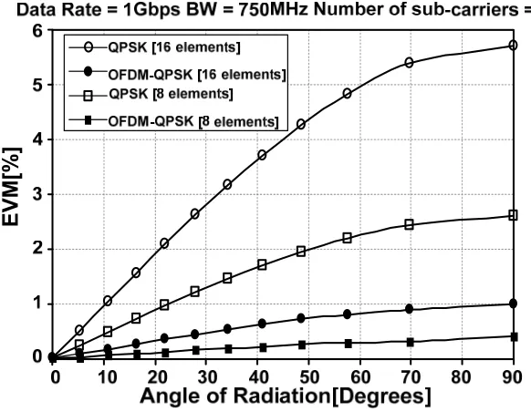
which is known a priori in the transmitter. The same normalization scheme can also be implemented in a phased-array receiver to account for similar signal distortion due to dispersion. Figure 2.10 compares the EVM for a raw QPSK modulation scheme and for a 64 sub-carrier OFDM-QPSK modulation scheme with complex normalization in a 24GHz phased-array transmitter with 8 elements and with 16 elements. The signal has a data rate of 1Gbps and a bandwidth of 750MHz. The maximum EVM, corresponding to a worst-case radiation angle of 90°, improves from 5.8% to 1%, in the 16 element case, demonstrating the efficacy of the normalized OFDM scheme. Thus, careful choice of modulation schemes and simple equalization methods can render the implementation of actual analog or digital delay in each element unnecessary. Increasing the number of sub-carriers decreases the EVM further and can compensate for increased distortion due to higher signal bandwidth and/or a higher number of elements in the array.
EV
M
[%
[image:44.612.172.463.416.642.2]]
2.7 Wireless Communication at Millimeter-Wave Frequencies
Larger available bandwidth and smaller physical system size motivate a move to high frequencies for wireless communications. In this section, the tradeoffs of wireless communication at millimeter-wave frequencies are discussed, with an emphasis on phased-array systems.
The beamforming and electronic beam-steering properties of phased-arrays provide a solution to the demand for directional wireless links at high frequencies. Resonance-based planar antennas such as dipoles or patch antennas are well-suited for an integrated phased-array based system with electronic beam steering. A typical patch antenna array at 24GHz, for instance, has an antenna gain of 8dB [55]. According to the antenna theorem, the aperture area of an antenna, for a given gain, decreases with an increase in frequency, reducing the power collected at the receiver at high frequencies [56]. The collected power cannot be increased by increasing aperture area, as that increases antenna gain, making the antenna more directional and hence limiting the angles at which radiation is possible. Thus, in a resonance-antenna based communication system, the advantage of large bandwidths at high frequencies is offset to some extent by the lower received power and the higher receiver noise figure at high frequencies. A quantitative analysis of this trade-off is detailed in this section.
For a transmit EIRP of PTX, the signal power at the receiver, PRX, is given by Friis’
equation [57] :
(
)
2
4
TX RX
RX TX l
G G
P P
d λ π
= , (2.11)
where GTX, GRX are receiver and transmitter antenna gain, λ is the wavelength, d is the
Shannon’s Theorem [58], is
2
.log (1 )
C= BW +SNR , (2.12) which is calculated for different carrier frequencies, fc, while keeping the fractional
bandwidth constant, accounting for larger bandwidths at higher frequencies. The noise figure of the receiver is assumed to increase linearly with frequency [59]. A noise figure of 3dB is assumed at 6GHz, resulting in a noise figure of 7dB at 24GHz.2 The individual antennas are assumed to be isotropic, and no excess path loss is considered (i.e., l=2). Figure 2.11(a) and (b) plot the channel capacity against carrier frequencies under the assumptions made above for two sets of EIRP and fractional bandwidth values. The fact that the curves are not monotonic and exhibit a peak demonstrates the tradeoff between larger bandwidths, lower collected power, and higher noise figure at high frequencies. The peak in the channel capacity curve moves to lower frequencies for higher transmitter-receiver separations and moves to higher frequencies with higher transmit EIRP or lower noise figure, both of which can be improved by implementing multiple-antenna systems such as phased-arrays. Figure 2.12 plots the channel capacity for different transmitter-receiver separations, assuming a bandwidth of 250MHz, EIRP of 30dBm, and receiver noise figure of 7dB at 24GHz. In a four-element phased-array receiver the SNR at the output may be improved by up to 6dB. When this improvement in SNR is included in (2.9) and (2.10), it can be seen that high-speed (greater than 1Gbps) phased-array data links are possible up to a distance of 200m at 24GHz.
2 Noise figure:
[
]
61 f GHz
(a)
(b)
Transmitter-Receiver Separation [m]
Shannon Capacity [Gbps]
0 100 200 300 400 500 600 700 800 900 1000
0 3.5
0.5 1 1.5
2 2.5
3 EIRPTX= 1W, BW = 250MHz NF = 7dB EIRPTX= 1W, BW = 250MHz
NF = 1dB (After SNR improvement due to 4-element Phased-array)
Figure 2.12 Channel capacity for different transmitter-receiver separations at 24GHz [53].
2.8 Chapter Summary
Silicon offers a new set of possibilities and challenges for RF and microwave applications. While the high cut off frequencies of the SiGe HBTs and the perpetual shrinking feature sizes of the MOSFETs hold a lot of promise, new design techniques needs to be devised to deal with the realities of these technologies, such as low breakdown voltages, lossy substrates, large interconnect parasitics, and high frequency coupling issues. To deal with the limitations and opportunities of this new paradigm, in high-speed and microwave design, it seems almost inevitable that new design methodologies that take advantage of multiple-signal paths, and distributed approaches will have to be applied more often. One example of such multiple signal path approaches is phased-array systems.
Chapter 3
A 24GHz, +14.5dBm Fully-Integrated Power Amplifier in 0.18μm CMOSA 24GHz, +14.5dBm Fully-Integrated
Power Amplifier in 0.18
μ
m CMOS
The quest for multi-Gigabit-per-second data rates in wireless networks has generated interest in the large bandwidth available at high frequencies. The Industrial, Scientific, and Medical (ISM) band at 24GHz has emerged as a viable candidate for gigabit-per-second wireless network solutions [36]. The allocation of the 22-29GHz band for wireless vehicular radar applications has added to the attractiveness of the frequency spectrum around 24GHz [35]. As a result, research on 24GHz band wireless technologies has accelerated, with receiver building blocks being demonstrated in GaAs pHEMPT [55] and SiGe BiCMOS [33][37]. A fully-integrated eight-element phased-array receiver in SiGe has also been reported at this frequency [60]. The implementation of these high-frequency systems in CMOS technologies will enable unprecedented levels of integration, making it possible to realize new architectures that combine microwave, analog, and digital circuitry on the same substrate at low cost. While there have been some recent efforts to implement building blocks above 20GHz on CMOS processes [61]-[64], the power amplifier (PA) reported in this chapter, and the fully-integrated four-element phased-array transmitter described in Chapter 4, represent the first efforts to integrate a complete multi-element transmitter with on-chip PAs in a CMOS process at 24GHz.
matching networks, followed by the measurement results presented in Section 3.4. Section 3.5 summarizes the results of this work.
3.1 Introduction
An integrated CMOS power amplifier at 24GHz presents several challenges. The two most important issues are the low unity power gain frequency, fmax,, of MOS transistors,
and the loss of on-chip passive elements, such as inductors and transmission lines, required for impedance matching. For narrowband amplifiers, where device capacitance is normally tuned out, fmax is a better metric for device speed than fT. In MOSFETs, fmaxis
limited primarily by the series gate resistance [64][65]. Generally, MOS transistors have lower fT and fmax as compared to SiGe bipolar transistors fabricated with the same feature
size [66]. In the 0.18μm process used in this design, the NMOS transistors, with an optimum layout, have an fmax of 65GHz, which is almost a factor of two smaller than the
fmax of their SiGe bipolar counterparts.
Lossy on-chip passives present another barrier to the full integration of a high-frequency PA. Skin effect results in larger ohmic losses in inductors and transmission lines at high frequencies. The skin depth in Aluminum at 24GHz is 0.5μm, which negates some of the advantages of a thick top metal layer, though the lateral sidewalls still help in reducing loss. Although Copper has better conductivity, in practice its performance can be additionally degraded by the cheese and fill rules necessary for stress relief during fabrication. As an example the cheese rule can increase the sheet resistance of a thick copper trace by a factor of two. Due to the relatively high conductivity of the substrate in most CMOS processes, the inductors and coplanar waveguide transmission line structures have substrate-induced losses as well. The combination of low active gain at high frequencies and high loss in impedance matching networks reduces the power gain of a single-stage amplifier. As a result, it becomes necessary to cascade an impractically large number of amplifier stages to achieve desired output power levels.
version of the slow-wave coplanar structure presented in [67]. This structure is used to design the fully-integrated 24GHz CMOS power amplifier described in this work.
3.2 Power Requirements in the 24GHz Band
The Federal Communications Commission (FCC) permits point-to-point wireless communication in the 24-24.25GHz band, subject to limitations on the transmitted power and directionality of the transmitter. At a distance of 3 meters from the transmitter, the maximum electric field permitted is 2.5V/m. This translates to an average effective isotropically radiated power (EIRP) of 29.7dBm.1 As discussed in Section 2.3, a phased-array transmitter could be employed to achieve the required EIRP and provide electronic beam steering capability. For an antenna array, the total gain is the product of the gain of each antenna and the array factor. The PA reported in this work is capable of generating up to +14.5dBm power at 24GHz. By using this PA in a 4-element phased-array system (that provides 12dB of array gain) with antennas that have at least 3dB gain, an EIRP of +29.5dBm can be achieved.
Figure 3.1 A 4-path phased-array transmitter for a 24GHz point-to-point wireless connection.
1
o
2η
2 E
S= , where S is power density, E is magnitude of electric field in space, and 377Ω
o o o = μ ε ≈
The FCC has also opened up 7 GHz of bandwidth from 22-29 GHz for vehicular shortrange radar (SRR) applications. In this case, there is an average radiated power limit of -41 dBm/MHz which if used over the entire 7 GHz bandwidth will correspond to an EIRP of -2.5dBm. Therefore, an amplifier designed for this application does not need to generate high output power and must instead be designed to have large bandwidth.
3.3 Circuit Design
This section describes the design evolution of the amplifier. First, the substrate-shielded coplanar waveguide structure, an important element in the design of the power amplifier, is presented. Next, amplifier stability and the design techniques used to achieve unconditional stability for all bias points will be discussed, followed by the design of the amplifier matching networks. Finally, the techniques used to minimize the effect of pad capacitances and wire-bond inductances will be described.
3.3.1 Substrate-Shielded Coplanar Waveguide Structure
At 24GHz, large capacitive coupling to substrate lowers the quality factor of the inductors, making inductor-based impedance matching networks lossy. On the other hand, this frequency is not high enough for direct application of standard transmission line structures. For example, in SiO2 dielectric, the wavelength (λ) at 24GHz is 6.3mm.
As shown in Figure 3.2(a), in coplanar waveguide (CPW) structures designed in CMOS processes with relatively high substrate conductivity (~10Ω.cm), capacitive coupling to the substrate is often the dominant source of high-frequency loss [68]. On the other hand, in the on-chip microstrip structure, shown in Figure 3.2(b), substrate-induced losses are minimal due to the shielding effect of ground plane. However, the close proximity of the
Substrate 0 0 0 0 Substrate Electric Field Gnd Substrate
Gnd Signal Gnd
Vias
Signa l Cur
rent
Retur n Cur
rent
Retur n Cur
rent
Retur n Cur
rent
Signal
Signa l Cur
rent
Retur n Cur
rent
(b) (a)
(c)
Gnd Signal Gnd
Shield #1
Signa l Cur
rent
Retur n Cur
rent
Retur n Cur
rent
Shield #2
ground plane to the signal