International Journal of Emerging Technology and Advanced Engineering
Website: www.ijetae.com (ISSN 2250-2459,ISO 9001:2008 Certified Journal, Volume 4, Issue 8, August 2014)
745
Digital Controller Design for Soft Switching ZCT Fourth Order
Boost Converter
Vaibhav Purwar
1, R. K. Pandey
2, Ankita Khare
3 1,2,3Kanpur Institute of Technology, Kanpur, IndiaAbstract—This paper presents a digital controller for Zero Current Transition (ZCT) turn-off Fourth Order Boost Converter (FOBC). The proposed converter uses soft switching technique which reduces the switching losses and increases the efficiency of FOBC. There are seven operating modes which have been analyzed. An attempt has been made to design a controller to regulate the output during input variation. The steady state characteristics of open loop controller is plotted. PSIM is used to verify the output. The output is regulated for input perturbation of 12 to 15 V and is verified by PSIM.
Keywords— Digital controller, Fourth Order Boost Converter, SMPS, Soft Switching, CTFBC.
I. INTRODUCTION
Earlier a number of soft switching PWM converters were used combining the features of PWM & resonating techniques reported in the literature [1]. Low power compact electronic circuit needs the use of High frequency switching converters. High frequency switching reduces the size and weight of the converters and also increases the power density. However, in hard-switching converters, as the switching frequency increases, switching losses and electromagnetic interference (EMI) increases.. To overcome this problem, soft-switching converters have been developed. Soft switching converters reduce the power losses improving the efficiency. Switches undergo a large number of losses during turn on & turn off. In ZVT-ON zero voltage switch on methodology has been analysed as reported in the literature [2]. DC-dc boost converters, as the name suggests, can deliver higher load voltages from the low voltage input. Earlier conventional boost converters were used for stepping-up the voltages but its full load efficiency is low on account of higher switching losses.
Recently, soft switching techniques are coming up to overcome switching losses which occurs in the conventional hard switching dc-dc converters and to get higher efficiencies at full load conditions. One such high gain soft switching converter topology is reported in the literature [3]. There are several advantages of fourth order boost converters over the conventional converters.
Earlier conventional DC-DC converters were used but it has large source current ripples which can be eliminated by Fourth order boost converter reported in the literature [4]. However, there is not enough work done on controllers for such kind of converters. This paper presents some investigations on digital controller design, which ensures load voltage regulation, rejecting source and load disturbances.
Earlier SMPSs were using Analogue controllers but digital controllers have many advantages over analogue controllers. High frequency conversion system make use of Digital controllers due to advancements in microcontrollers and digital signal processors. Several compensator design approaches have been reported in literature for Op-Amp or IC based analogue controllers. In the digital controller design there are two main approaches that are widely used (i) Digital Redesign method (DRM) (ii) Direct Digital Design method (DDDM). In the first method, the compensator is designed by using s-domain transfer function together with linear system theory and the resulting compensator is transformed into digital domain using appropriate z-transformation. While in case of DDDM method the compensator is designed in z domain itself and there is no s to z transformation is required. Here, DDDM method is used for digital controller design. In this paper zero current transition is introduced into the Fourth order boost converter.
II. ZERO-CURRENT TRANSITION FOURTH ORDER BOOST
CONVERTER
The zero-current transition fourth-order boost converter is shown in Fig. 1. In addition to the conventional boost converter, this topology uses two energy storage elements, one capacitor and one inductor to realize lower ripple currents. To realize soft-switching a zero-current transition network is added as shown in the circuit diagram and is reported in literature [5].The proposed converter exhibits seven operating modes, in one switching cycle and the status of the switch is given in the
International Journal of Emerging Technology and Advanced Engineering
Website: www.ijetae.com (ISSN 2250-2459,ISO 9001:2008 Certified Journal, Volume 4, Issue 8, August 2014)
746
L2
L1
Vg
L3 Lr
Cr C1 C0 Rload
DM
DA
SM SA
Fig.1 Zero-Current Transition Fourth order Boost Converter
A. Status of the switch modes
Mode-I (t0<t<t1)
On writing KCL at input node
I
g
i
L3
i
DM (1)On differentiating and applying KVL at input node
3
3 1
L c di
L v
dt (2)
3 3
2
2 2
O L
L V L di
di
dt L L dt (3)
1 2
1 2
1 2 1 2 3
1 1
C O c
d v V v
dt C L C L L
(4)
Transforming into Laplace domain,
0 3 0 3
1 2 2
2 3 2 3 1
( )
( ) ( ) ( )
C
V L V L s
v s
L L s L L s
(5)
Where, 2 3
1
1 2 3
.
( )
L L
C L L
Transforming these equations into time-domain
3 1
1
2 3
1 ( )
( ) VoL Cos t
vc t
L L
(6)
0 0
3 1
2 3 1 2 3
( ) sin
( ) ( )
L
V V
i t t t
L L L L
(7)
The second part of the equation is negligibly small and can be ignored
1 0 0 1
1
2 3 1 2 3
( ) sin
( ) ( )
DM g
V V
i t I t t
L L L L (8)
The time duration of this mode is given as
2 3
1
0 g
L L
t I
V
(9)
Mode-II (t1<t<t2)
In this mode a steady state current Ig flows through the main switch.
During this mode the main diode voltage will be
3 3 0
L C DM
v v v (10)
At the end of this mode auxiliary switch will be given firing pulses, therefore,
2 Saux s
t =(D-D )T (11)
Here, D=Main switch duty ratio, and DS aux= Auxiliary
switch duty ratio
Mode-III (t2<t<t3)
This mode operates on switching ON the auxiliary switch
3(0) g L
i I
(12)
0
(0)
cr
v V (13)
(0) 0
Lr
i (14)
On KVL/ KCL,
cr Lr
v v (15)
r
r c
L
i
i
(16)On Substituting (16) in (15)
2
2 0
cr cr
r r
v d
L c v
dt (17)
On solving the above equations with initial conditions
we get
1 1
0
( ) os
cr C r
v t V
t (18)
1 0 sin( 1)Lr r
r V
i t t
Z
(19)
Where
1
r
r r
L c
, r 1
r r
and Z C
, r
r r L also Z
C
Mode of operation
Time duration
SM SA DM DA
mode1 t0<t<t1 ON OFF ON OFF
mode2 t1<t<t2 ON OFF OFF OFF
mode3 t2<t<t3 ON ON OFF OFF
mode4 t3<t<t4 ON ON OFF ON
mode5 t4<t<t5 OFF OFF OFF ON
mode6 t5<t<t6 OFF OFF OFF ON
International Journal of Emerging Technology and Advanced Engineering
Website: www.ijetae.com (ISSN 2250-2459,ISO 9001:2008 Certified Journal, Volume 4, Issue 8, August 2014)
747
At
t
t
3 , at the end of this modev
cr( )
t
3
0
3 2
2 r r
t t L c (20)
3 2
2
r r
t t L c (21)
This mode ends at t=t4 and the next mode begins
Mode-IV (t3<t<t4)
Initial conditions:
3(0)
L g
i I
(22) (0) 0 cr v (23) 0 (0) Lr r V i Z (24)
2(0) 0
L
v (25)
On applying KCL/KVL,
3 2
L DA L
i
i
i
(26)Lr cr
v v (27)
3 ( )
cr
L g Lr r
dv
i I i c
dt
(28)
Solving the above equations results in
2 2 3 1 1 0 cr cr r r
d v v
dt C L L
(29) On solving
3 2
1 3 1
3
sin ( )
( ) o r r r in
cr O
r r r
V t t c L L
v t s t
L L L c (30) 3 3 , r o r r L L where
c L L
3
3 , r eq r L L L L L 1 , o r eq andAlso C L
0 3 2
1 0 3 3 ( ) ( ) 1 r cr r
V sin t t
v t sin t t
L L (31)
Main switch current is given by
3 2
3
3 3
sin
1 ( )
1
o r
g o
r o
V t t
I cos t t
L L L (32)
3 2
0 3 3 3 3 sin
1 ( )
1 r g o r o t t V
I Cos t t
L L L L (33) 3 3 1 4 3 3 2 1 / 1 1 ( )
g o r
o o r
I L L L
t t cos
V Sin t t (34)
Mode-V (t4<t<t5)
During this mode,
v
Lr
v
cr (35)
0 3 2
1
3 3
sin ( )
( ) sin
1
t r o
Lr o
r r t
r
V t t
v
i t t
z L L L
(36)At the end of this mode at
t
t
55
( ) 0
Lr
i t , (37) On solving,
3
1 5 3 3 2 1 / 1 1
sin ( )
o r
o r r
L L
t t Cos
t t
(38)
Mode- VI (t5<t<t6)
At the end of this mode, at t=t6, when vcr charges up to
Vo, main diode comes into conduction, i.e.
6
( ) 0,
Dmain
v t
3 21
3 5
3
sin ( )
( ) sin ( ) ( )
1
g
o r
DM O o
r r
I
V t t
v t V t t t t
C L L
as , vDM( )t6 0, (39)
3 2
6 3 5
3 sin ( )
0 sin ( ) ( )
1 g o r O o r r I
V t t
V t t t t
C L L (40)
The time duration of this mode is
3 2
5 4
6 5
3
sin ( - ) sin
-( 1 / )
r o
r o o
g r
t t t t
t t C V V
I L L
(41)
Mode-VII (t6<t<Ts)
During this mode main diode current reaches a steady state value and this mode continues till the main switch is turned ON.
At,
7 s
International Journal of Emerging Technology and Advanced Engineering
Website: www.ijetae.com (ISSN 2250-2459,ISO 9001:2008 Certified Journal, Volume 4, Issue 8, August 2014)
748 III. CONTROL OF ZCTFOURTH ORDER BOOST
CONVERTER
The Fig. 2. shows the block diagram of the closed loop converter system. It gives the stable output under varying input and output condition.
Controller Gc(z)
Fourth Order Boost Converter
Vo
Vref
Fig. 2. Closed Loop ZCT Fourth Order Boost Converter
The structure of the controller is,
2
2 1 0
2
2 1 0
( )
c
a z a z a
G z
b z b z b
(43)
The above expression can be represented in pole-zero form as follows
11 22
( ) c
z Z z Z
G z
z P z P
(44)
Where, Z1 and Z 2 are zeroes and P1 and P2 are the poles
of the compensator.
IV. SIMULATION RESULTS
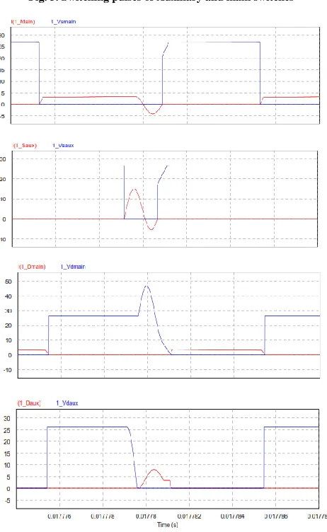
To verify the analysis and the proposed design a ZCTFBC system with the following parameters is designed: L1=130 µH, L2=48µH, L3=1.29 µH, Lr=0.5 µH, C1=98 µF, C2=96 µF, Cr=173 nF, R=19.2Ω and fs=100kHz. The switching pulses of main & auxiliary switches are shown in Fig. 3.The effectiveness of the controller has been verified in simulation for various load and source side disturbances. Load disturbance of load resistance from 36 to 20 Ω has been created after 10 ms and the controller action made the converter to regulate the voltage with in 3 ms. Sudden disturbance in the source voltage of 12 to 15 V has been created in the source voltage and also found the controller action to be satisfactory which made the transients to die down with in 3 ms. The corresponding results are shown below. Its steady state waveforms are shown in Fig. 4. And dynamic response is shown in Fig. 5. PSIM [6] is used for the verification of results.
[image:4.612.330.561.304.680.2]Fig. 3. Switching pulses of Auxiliary and main switches
International Journal of Emerging Technology and Advanced Engineering
Website: www.ijetae.com (ISSN 2250-2459,ISO 9001:2008 Certified Journal, Volume 4, Issue 8, August 2014)
749 Fig.5. Simulated Dynamic response characteristics of ZCTFBC
(Vg=12 to 15V & R=36 to 20Ω)
IV. CONCLUSION
In this paper Zero-Current transition switching Fourth order boost converter was presented and its modes of operation were explained with mathematical expressions.
Its open loop response and closed loop response are analyzed. The graphs showing the ZCS condition is depending up on the duty ratio, soft-switching capacitance/Inductor, Load and duty ratio of switches gating pulses. Digital controller open and closed loop characteristics are plotted using PSIM. The designed controller is providing load voltage regulation for perturbations in load and source parameters.
REFERENCES
[1] Guichao Hua, Eric X. Yang, Novel Zero-Current-Transition PWM converters, IEEE 1994, 601-606.
[2] Devasy Sachin, Digital voltage mode controller for soft switching ZVT-ON Boost converter, Proc of IEEE, 1-5.
[3] Mummadi Veerachary, Ruddireddy Sekhar, Voltage mode controller design for soft switching High gain boost converter, IEEE Proc on PEDES2010, Dec 2010, 1-5.
[4] Veerachary M, Anmol Ratna Saxena, Design of Robust digital Stabilizing controller for Fourth order boost dc-dc converter, A Quantitative Feedback Theory Approach, IEEE Trans, Jan 2011, vol 58, 263-277.
[5] Mummadi Veerachary, Mallesham Myla, Digital voltage mode controller for zero-Current Transition Fourth Order Boost Converter, IEEE 2013, 1150-1155.
[6] PSIM User Manual