2019 International Conference on Information Technology, Electrical and Electronic Engineering (ITEEE 2019) ISBN: 978-1-60595-606-0
Research and Implementation of Charging and Discharging Device
Based on DSP Bi-directional DC-DC Converter
Shen FENG, Ting-hui LI* and
Zhi-xian LIAO
Guangxi Normal University, Guilin of Guangxi, China
*Corresponding author
Keywords: Two-stage LC filtering, Buck - Boost, Double current loop, High precision, Digital power.
Abstract. With the development of new energy, the charge and discharge technology of battery is very important. Bi-directional buck-boost circuit is used as the circuit topology to realize bi-directional flow of energy. Two-stage LC filter circuit is adopted and current double-closed loop is used to reduce the current ripple of battery charging and discharging and improve the accuracy of charging and discharging current. This paper first simulates its circuit and algorithm with PSIM, and then makes a 300W prototype with TMS320F28335 DSP as the main control chip. The current accuracy obtained by simulation and prototype experiment is 0.00mA and 0.75mA, respectively. The test results show that the precision error of double current ring is small.
Introduction
Since the 1970s, the high-frequency switching power supply composed of high-frequency switching dc-dc converter technology has gradually replaced the linear regulated power supply. At the end of the 20th century, driven by the demand of IT and communication industry, dc-dc switching converter technology and industry developed rapidly. In the 21st century, the trend of green energy, new energy generation, energy storage are inseparable from dc-dc switch converter. At present, Chinese rapid economic development, continuous progress in science and technology, battery is a kind of new energy, and its price is low, stable power supply and other advantages, is widely used in electric cars, battery cars, power supply equipment, UPS and other fields. Therefore, the research on charge and discharge of battery is a hot topic in recent years. Using reasonable and stable current to charge and discharge the battery can maximize its energy utilization, reduce the damage to the battery and improve its service life. Although the accuracy of analog power is relatively high, it is difficult to upgrade, large volume and severe temperature fluctuation. Compared with digital power, it has the advantages of simple upgrade, easy secondary development, small size and stable system. In the process of charging and discharging the battery, the bi-directional dc-dc converter regulates the energy so that the bus voltage and the energy at both ends of the battery can flow bidirectionally. The second-stage LC circuit itself can filter out harmonics, but the accuracy of the ADC acquisition within DSP cannot reach, so, in view of this problem, the sampling accuracy can be improved through the acquisition of the external 24-bit ADC chip, and the double-loop control makes the output accuracy meet the requirements.
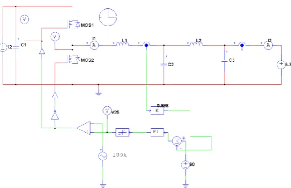
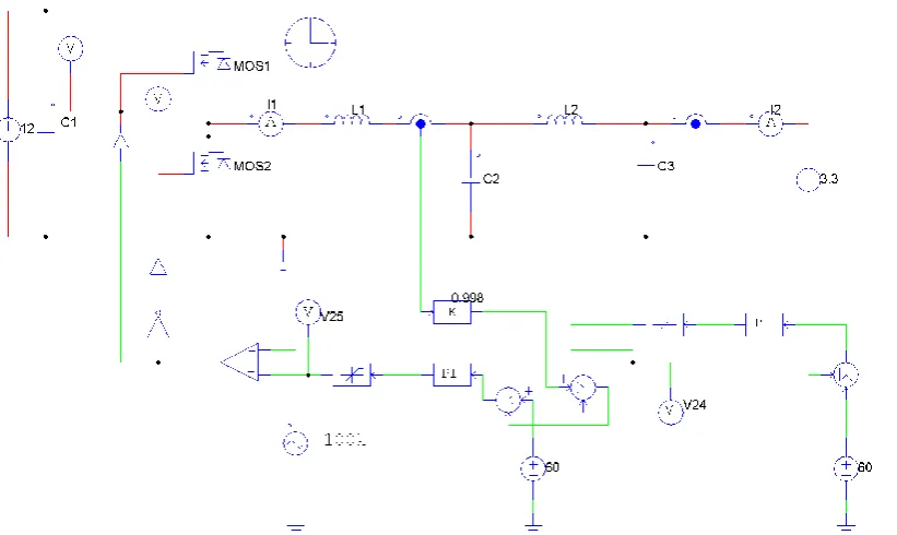
Bi-directional DC-DC Converter Topology
Working Principle
plays the main control, the circuit is in Buck mode, while when S2 plays the main control, the circuit is in Boost mode. The Bus terminal is the input terminal of the Bus and the Out terminal is the battery terminal.
Figure 1. Circuit topology of bidirectional dc-dc converter.
Calculation of Main Circuit Parameters
Because bi-directional dc-dc converters can work in Buck mode or Boost mode, it can be design only one of them when designing circuit parameters. The following study only Buck converter, can get two-way dc-dc circuit parameters. It consists of a switch tube, a diode, an inductance and a capacitor. The ratio of switching time
t
on to switching period
T
S is defined as duty cycle DC, which is expressed
as: T t D S on C (1)
According to whether the inductance current is continuous or not, Buck converter has three operating modes: continuous conduction mode, intermittent conduction mode and critical mode. Critical mode is the mode between continuous mode and intermittent mode. When the inductance current is continuous, the output ripple is small and the filter design is simple. The increment of linear increase of inductance current is: T D U U t U U dt L U U
i C S
S S
L L
t S
L 1 0
0 1 0 0
(2)
US is the input voltage,UO
is the output voltage, L is the inductance,t1 is the rise time of the inductive
current,D
C is the duty cycle of switch tube closure. The absolute value of linear decrease of the inductive
current is: T D U t t U dt L U
i L L C S
t
L 1 2 0(1 )
0( )
2
0
0
(3)
In the formula, t2 is a switch tube switch time.
I iL2 0
(6)
R U I0 0
,R is the load.
The simultaneous equations (5) and (6) obtain the inductance of the critical state:
T P D U T I D U T R D
L S S S
C C C 2 0 0 0 0 2 ) 1 ( 2 ) 1 ( 2
1
(7) Where R U P 0 0
is the output power. The voltage
UO
generated by charging the capacitor by the current
I
i
i
c
L
0 flowing through the capacitor is called ripple voltage, and its expression is:T LC
D U
UO O C S2 8 ) -1 (
,So circuit capacitance:
T U L D U C S O C O 2 8 ) -1
( (8)
Experiment and Conclusion
Simulation
Figure 2. Single current loop simulation diagram.
Figure 3. Single current loop charging current waveform. Figure 4. Single current loop discharge current waveform.
Figure 5. Simulation circuit model diagram.
Figure 6. Current double loop charging current waveform. Figure 7. Current double loop discharge current waveform.
Experimental Verification
Experimental Circuit
EMI
Bi-directional dc-dc
converters LOAD
Signal acquisition and algorithm
processing Auxiliary
power
Driver
circuit Sampling
12V
DSP
DC-DC Out and load
Input
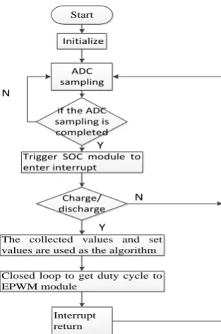
Start
Initialize
ADC sampling
Trigger SOC module to enter interrupt
if the ADC sampling is completed
Interrupt return
N
Y
Charge/ discharge
The collected values and set values are used as the algorithm
Y N
[image:6.595.367.524.75.311.2] [image:6.595.55.323.152.312.2]Closed loop to get duty cycle to EPWM module
Figure 8. Bi-directional dc-dc circuit structure based on DSP. Figure 9. Main software flow chart.
Software Process
TMS320F28335 single-chip microcomputer is a floating-point single-chip microcomputer, the speed of calculation, the peripheral interface, often used by industrial switching power supply. Although the sampling accuracy of 16-bit external ADC is high, the sampling speed is slow. Although the sampling speed of internal ADC is fast, the sampling accuracy is not high enough. Therefore, high precision outer ring and fast speed inner ring are adopted to compensate each other to improve current accuracy. The sampling point is set at the junction of increase first and decrease later. At this time, the inductance current is relatively stable. The interrupt is then triggered to enter the operation function and the duty cycle is given to the EPWM module to drive the switch tube. The software flow chart is shown in Figure 9.
Sampling Design
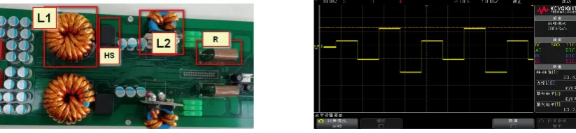
[image:6.595.110.459.597.747.2]Experimental Results
Figure 11 is the bi-directional dc-dc prototype picture. There are two channels of bi-directional dc-dc on this PCB. Figure 12 is the output current waveform of battery charge and discharge switching. By using high-precision measuring instrument, the set value is 60A when charging the battery, and the two-way dc-dc output current is 60000.25 to 60000.75 mA. When discharging the battery, the set value is -60A, and the output current of two-way dc-dc is -59999.98 to -60000.65mA. When using a single current ring, the error accuracy is between 1.00-3.00mA, and that of a double current ring is 0.75mA. Therefore, the use of a double current ring improves the accuracy of output current, so as to charge and discharge the battery in a more balanced and safe way and improve the service life of the battery.
[image:7.595.97.509.209.304.2]
Figure 9. Prototype images. Figure 10. Charge-discharge switching output current waveform.
Conclusion
In this paper, the topology of Bi-directional dc-dc circuit is analyzed, and the double-current loop control of two-stage LC circuit is tested by simulation, so that the output current fluctuates around the set value, which is more accurate than the traditional single-loop control. Using TI company's floating-point DSP TMS320F28335 as the controller, a 300W prototype is made. When the output is 60A, the precision error is smaller than that of the single-loop control. The external loop current sampling accuracy is high, and the inner loop current sampling speed is fast.
The Bi-directional dc-dc power supply with double current loop can charge and discharge the battery quickly and safely. Experimental results show that this circuit topology and control method can be applied to the battery charging and discharging power supply.
References
[1] B Mallikarjuna Reddy, Paulson Samuel. A Comparative Analysis of Non-Isolated Bi-directional DC-DC Converters, J.IEEE 1st International Conference on Power Electronics.2016.
[2] KS Alam, LAR Tria, D Zhang, etc. Design of a bi-directional DC-DC converter for Solid-State Transformer (SST) application by exploiting the shoot through mode, J. IEEE International Conference on Sustainable Energy Technologies. 2016.
[3] Gang Liu, Dan Li, Yungtaek Jang. etc. Over 300kHz GaN device based resonant bidirectional DCDC converter with integrated magnetics, J. Research Gate. March 2016.
[4] Haitao Hu, Xianyi Cheng, Jianshan Wang, etc .Control and simulation of bi-directional DC/DC converter for 5KW distributed wind/solar hybrid system., J. Chinese Control and Decision Conference. 2017.
[5] Peng Liu, Changsong, Chen, Shanxu, Duan .etc. A Dual Phase-Shifted Modulation Strategy for the Three-Level Dual-Active-Bridge DC-DC Converter, J.IEEE Transactions on Industrial. PP(99):1-1 April 2017.
[7] Guodong Liu, Zhipo Ji, Ruichang Qiu, etc. The Research on Bi-Directional DC/DC Converter for Hybrid Power System, J.Part of the Lecture Notes in Electrical Engineering book series.2018