N A N O E X P R E S S
Open Access
Amorphous silicon nanocone array solar cell
Subramani Thiyagu, Zingway Pei
*and Ming-Sian Jhong
Abstract
In the hydrogenated amorphous silicon [a-Si:H]-thin film solar cell, large amounts of traps reduce the carrier’s lifetime that limit the photovoltaic performance, especially the power conversion efficiency. The nanowire structure is proposed to solve the low efficiency problem. In this work, we propose an amorphous silicon [a-Si]-solar cell with a nanocone array structure were implemented by reactive-ion etching through a polystyrene nanosphere template. The amorphous-Si nanocone exhibits absorption coefficient around 5 × 10⁵/cm which is similar to the planar a-Si:H layer in our study. The nanostructure could provide the efficient carrier collection. Owing to the better carrier collection efficiency, efficiency of a-Si solar cell was increased from 1.43% to 1.77% by adding the nanocone structure which has 24% enhancement. Further passivation of the a-Si:H surface by hydrogen plasma treatment and an additional 10-nm intrinsic-a-Si:H layer, the efficiency could further increase to 2.2%, which is 54% enhanced as compared to the planar solar cell. The input-photon-to-current conversion efficiency spectrum indicates the efficient carrier collection from 300 to 800 nm of incident light.
Keywords:Nanocone, amorphous silicon, solar cell
Introduction
The solar energy is a renewable energy and is expected to alleviate the progress of global warming. However, the cost to produce electricity by solar energy harvesting is still higher than the traditional method, such as ther-mal power generation by burning coal and petroleum or the hydro-electrical power generation. Thin-film silicon solar cell is one of the candidates to achieve low cost requirement. However, to achieve low cost, the low-tem-perature process makes the thin-film silicon generally be in the form of microcrystalline or becomes amorphous. In this structure, large amounts of traps reduce the car-rier’s lifetime that limit the photovoltaic performance, especially the power conversion efficiency. The nanowire structure is proposed to solve the low efficiency problem [1]. The light harvesting is along the wire and the car-rier collection is along the radial direction. The path for photo-carrier collection and light harvesting is perpendi-cular. Longer wire could ensure that the solar light be harvested thoroughly while maintaining the efficient car-rier collection. Among all materials, the hydrogenated amorphous silicon [a-Si:H] nanowire solar cell has been particularly investigated and predicted to have better
photovoltaic performance over planar solar cell [2]. Additional to the efficient carrier collection, the nanos-tructure surface was expected to have light-trapping behavior that could further increase the total amount of solar energy harvesting in a short nanowire [3-5]. These advantages cause the nanowire solar cell to largely improve the efficiency compared to planar solar cell. However, the randomly grown Si nanowires by bottom-up method are hardly to manufacture a good solar cell device that has higher photovoltaic performance on Si nanowire than planar one is rarely reported [6-8]. More-over, the combination of the efficient carrier collection and light trapping limits the understanding of the elec-trical advantages of nanowire solar cell itself. In this work, we prepare the a-Si:H nanostructure by reactive-ion etching [9-12] through a closely packed nanosphere template [13]. In previous study, the low aspect ratio nanocone a-Si:H has negligible light-trapping effect [14]. The light illuminated through glass side instead of sur-face of the a-Si:H nanocone to make the effect of light-trapping negligible To explore the advantage of the nanostructure, four types of a-Si:H were used to fabri-cate a-Si:H solar cell. The first one is the planar solar cell without nanostructure used as a reference. The sec-ond one is an intrinsic-a-Si:H nanocone solar cell. The third is an intrinsic-a-Si:H nanocone solar cell with H2 plasma treatment for 10 min prior to N+-a-Si:H * Correspondence: [email protected]
Graduate Institute of Optoelectronic Engineering, Department of Electrical Engineering, National Chung Hsing University, Taichung, 40227, Taiwan, Republic of China
deposition. The last one is also an intrinsic-a-Si:H nano-cone solar cell with additional 10 nm a-Si:H layer after H2 plasma treatment.
Experimental method
Figure 1 depicts the schematic structure of the proposed a-Si:H random nanocone solar cell. The process flow to fabricate the a-Si:H random nanocone solar cell is described as follows. In the first step, the P+and instrin-sic a-Si:H, 50- and 200-nm thick, respectively, were grown on a cleaned indium-tin oxide/glass substrate by plasma-enhanced chemical vapor deposition [PECVD] at 130°C. A template containing nanospheres was prepared on top of the a-Si:H by nanoscopic phase separation of poly(styrene-block-methyl methacrylate) [PS-b-PMMA] diblock copolymer. The PS-b-PMMA powder was dis-solved in toluene at a concentration of 20 mg/ml. After stirring overnight, the PS-b-PMMA solution was spin-coated on the a-Si:H and was annealed at 180°C for 24 hours to initiate nanophase separation. The PS-b-PMMA films were then immersed in a heated acetic acid at 80°C for 20 min to form the polystyrene [PS] nanospheres. After PS nanosphere formation, the sample was thoroughly rinsed with deionized water and dried in an nitrogen-filled environment. The diameter of the nanospheres is approximately 30 to 50 nm. This tem-plate pattern was transferred to the a-Si:H by reactive ion etching [RIE]. The etching power was 250 W with CF4 and O2 as the etching gasses with a ratio of 20:1. The ratio of etching rate for a-Si:H and PS in CF4/O2 plasma is approximately 4.5:1. As a result, by carefully controlling the PS thickness (approximately 30 nm), the PS could be completely removed leaving a-Si:H nanos-tructure. The atomic force microscopy surface morphol-ogy of the obtained a-Si:H nanostructure is shown in Figure 2. A random cone-shaped nanotexture was
[image:2.595.305.539.86.300.2]obtained. The reason of the randomly distributed cone-shaped nanostructure is believed due to the lateral che-mical etching of a-Si:H under the PS nanospheres and the gradual shrinkage of the size of the PS nanospheres themselves. The height of the random nanocone is approximately 150 nm. With the roughly 30- to 50-nm diameter of the cone tip, the aspect ratio is approxi-mately 3 to 5. The bottom of each a-Si:H-random nano-cone is still connected by the P+a-Si:H layer. After a-Si: H-random nanocone formation, the 45-nm thick N+ a-Si:H was grown in a PECVD chamber at 130°C. The H2 plasma treatment was carried at a radio-frequency power of 20 W for 10 min to remove native oxide and passivate the a-Si:H surface. Finally, an Al layer of 100-nm thick was deposited by thermal evaporation as the cathode of the solar cell. Enlarged part of the a-Si:H nanocone structure is also schematically shown in the Figure 1 to describe the photogeneration and transport mechanism. While the light was illuminated to the a-Si: H layer, the photon was absorbed and generated elec-tron-hole pair. The hole moved toward the bottom P+ a-Si:H as in the planar cell. However, the electron moved to the N+-a-Si:H layer, nearly perpendicular to the hole movement direction. The electron moving in a short distance than planar cell might cause an efficient collection efficiency for electron that enhances the photocurrent.
Results and discussion
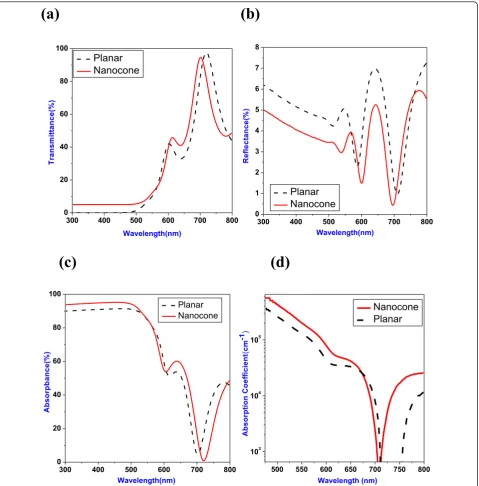
An ultraviolet-visible-near infrared spectrometer was used to explore the optical behavior of a-Si:H nanocone. Figure 3a depicts the transmittance of a-Si:H planar and
ITO/Glass P+ a-Si (50nm)
a-Si Nanostructure Al
[image:2.595.58.290.543.690.2]hv
Figure 1The schematic structure for a-Si:H-nanocone solar cell. Enlarged part of the a-Si:H-nanocone structure describes the photogeneration and transport mechanism.
Figure 2The AFM surface morphology of a-Si:H nanocone. The
nanocone layer. At the wavelength less than 500 nm, the low transmittance [T0] indicates the high absorption of a-Si:H. The surface reflectance will affect the amount of light absorption; therefore, the reflectance [R] spectrum was measured and depicted in Figure 3b. For both pla-nar and nanocone a-Si:H, they exhibit similar transmit-tance and reflectransmit-tance. Consequently, the absorbance [A] (%), which is calculated throughA = 1-R-T0 and was depicted in Figure 3c, has similar behavior for planar
and nanocone structure. There is no light-trapping behavior in the a-Si:H random nanocone with low aspect ratio [14]. By taking the reflectance [R] and trans-mittance [T0] spectra into account, the absorption coef-ficient can be calculated by the following equation:
T= T0
(1−R) =e
−α×d (1)
(a)
(b)
300 400 500 600 700 800
0 20 40 60 80 100
Tr
ansm
it
ta
nce(
%
)
Wavelength(nm) Planar
Nanocone
300 400 500 600 700 800
0 1 2 3 4 5 6 7 8
R
e
fle
c
ta
n
c
e
(%
)
Wavelength(nm)
Planar Nanocone
(c)
(d)
300 400 500 600 700 800
0 20 40 60 80 100
Absor
pbance(
%
)
Wavelength(nm) Planar Nanocone
500 550 600 650 700 750 800 103
104
105
A
b
s
o
rp
tio
n
C
o
e
ffic
ie
n
t
(
cm
-1)
Wavelength (nm)
[image:3.595.60.540.88.575.2]Nanocone Planar
, in which T is the absolute transmission, a is the absorption coefficient and d is the thickness of the intrinsic-a-Si:H layer. Figure 3d depicts the absorption coefficient of planar and nanocone a-Si:H layer. The absorption coefficient for the a-Si:H nanocone is approximately 5 × 10⁵/cm at 500 nm which is slightly higher than the planar structure. The effect of the differ-ence in total amount of light harvesting between planar and nanocone solar cell while exploring the carrier col-lection efficiency can be minimized by light illumination through the glass side.
The photovoltaic properties of a-Si:H solar cell was measured by solar simulator under air mass 1.5 G con-dition. Figure 4a shows the photocurrent density-voltage behavior. The planar pin a-Si:H solar cell exhibit short-circuit current density [Jsc] of 5.0 mA/cm2 and power conversion efficiency [PCE] of 1.43%. The detailed photovoltaic properties were listed in Table 1. With sur-face nanocone structure, the Jsc increases to 5.7 mA/ cm2 which is 14% enhanced. Additionally, the PCE also increases to 1.77% which is 24% enhanced. The short transport path for the electron in the a-Si:H nanocone contributes the additional 0.7 mA/cm2 photocurrent [2]. However, the native oxide and defects on the a-Si:H nanocone after RIE etching may either restrict part of photocurrent transport or act as recombination centers that increase the series resistance as high as 160Ω·cm2. The H2 plasma was used to remove the native oxide and passivate the defects. After treating the a-Si:H nano-cone surface by H2 plasma, the native oxide was removed and the surface defects were passivated [15,16]. This could be understood by the dark current as shown in Figure 4b. The reverse leakage current density was largely reduced after plasma treatment. The series resis-tance also reduces to around 60 Ω·cm2. Additionally, the Jsc further increases to 5.8 mA/cm2. The PCE is 2.0%, approximately 40% enhanced over planar solar cell. Another way to reduce the interface state defect density is to cover the surface by a layer of intrinsic a-Si:H. The 10-nm intrinsic a-Si:H was grown after H2 -plasma treatment. With this additional layer, Jsc further increases to 5.9 mA/cm2. The PCE increases to 2.2%, approximately 54% enhanced over planar solar cell. Further analysis of the nanocone solar cell by input photon-to-electron conversion efficiency [IPCE] spec-trum could investigate the photoresponse at each wave-length. Figure 5 shows the IPCE results. At short wavelength, the surface was passivated. The higher elec-trical field in the nanocone structure [17] accelerates the carrier transport that reduces recombination. As a con-sequence, there is an increase in the IPCE. At long wavelength, the better carrier collection efficiency of the nanocone structure ensures the higher IPCE as com-pared to the recent publication on the a-Si PIN solar
cell with nanodome surface which exhibits efficient light management [18], achieving extensive solar energy con-version efficiency. This work mainly focuses on the
(a)
0.0 0.2 0.4 0.6 0.8 1.0
0 1 2 3 4 5 6 7 8
Phot
ocurrent
densi
ty
(m
A
/c
m
2 )
Voltage(V) PI / N+ Planar Cell P / I(Nanocone) / N+)
P / I(Nanocone)+H2 Plasma / N+)
P / I(Nanocone)+H2 Plasma+10nm / N+)
(b)
-1.0 -0.5 0.0 0.5 1.0
10-9 10-8
10-7
10-6 10-5 10-4
10-3
10-2
Dar
k Cur
rent
(
A
/cm
2
)
Voltage (V) PI / N+
P / I(nanocone) / N+
P / I(nanocone) / H2 plasma / N+
[image:4.595.305.539.87.567.2]P/I (nanocone)/H2 plasma/i (10nm)/N+
Figure 4The current density-voltage characteristics. Solar cells with 200-nm thick planar-a-Si:H film, 200-nm thick a-Si:H nanocone,
200-nm thick a-Si:H nanocone with 10-min H2plasma treatment,
and 200-nm thick a-Si:H nanocone and additional 10-nm a-SiH layer
after 10 min H2plasma treatment. (a) Photovoltaic properties under
AM 1.5 G light illumination (PI/N+planar cell, circle with center dot;
P/I nanocone/N+, red square; P/I nanocone + H2plasma/N
+
, green
circle; P/I nanocone + H2plasma + 10 nm/N
+
, blue square) and (b)
under dark condition (PI/N+, black square; P/I nanocone/N+, red
circle; P/I nanocone/H2plasma/N+, green triangle; P/I nanocone/H2
transport part. Without light-trapping efficient in nano-cone structure, the photocurrent enhancement supports the assumption of efficient carrier collection by the nearly perpendicular light absorption and carrier trans-portation in nanostructure.
Conclusions
In this work, we propose an amorphous silicon [a-Si] solar cell with a nanocone-array structure which were implemented by PS nanospheres as template for RIE dry etching. The amorphous Si nanocone exhibits 5 × 10⁵/ cm absorption coefficient which is similar to the planar a-Si:H layer in our study. The proposed nanocone solar cell could have better carrier collection efficiency and implies an efficiency of 1.77% for a-Si nanocone solar cell which has 24% enhancement over planar solar cell (1.43%). With hydrogen plasma treatment and additional 10-nm a-SI:H layer, the efficiency further increased to
2.2%, which is 54% enhanced as compared to the planar solar cell. This indicates that the a-Si nanostructure could efficiently enhance the photocurrent of the thin-film solar cell.
Abbreviations
a-Si: amorphous silicon; IPCE: input photon-to-electron conversion efficiency; Jsc: short-circuit current density; PCE: power conversion efficiency; PECVD: plasma enhanced chemical vapor deposition; PS: polystyrene; RIE: reactive ion etching; SEM: scanning electron microscope.
Acknowledgements
We thank the National Science Council for the financial support under the grant NSC-99-ET-E-005-001-ET.
Authors’contributions
ZP conceived of the study, participated in its design and coordination, and revised the manuscript. ST drafted the manuscript and carried out the experiments on fabrication of PS nanosphere and optical characterization. MSJ carried out the PECVD experiments. All authors read and approved the final manuscript.
Competing interests
The authors declare that they have no competing interests.
Received: 28 November 2011 Accepted: 6 March 2012 Published: 6 March 2012
References
1. Kayes BM, Atwater HA, Lewis NS:Comparison of the device physics
principles of planar and radial p-n junction nanorod solar cells.J Appl
Phys2005,97:114302-114311.
2. Pei Z, Chang ST, Liu CW, Chen YC:Numerical simulation on the
photovoltaic behavior of an amorphous-silicon nanowire-array solar cell.
IEEE Electron Device Lett2009,30:1305-1307.
3. Hu L, Chen G:Analysis of optical absorption in silicon nanowire arrays
for photovoltaic applications.Nano Lett2007,7(11):3249.
4. Thiyagu S, Devi BP, Pei Z:Fabrication of large area high density, ultra-low
reflection silicon nanowire arrays for efficient solar cell applications.
Nano Res2011,4(11):1136.
5. Pei TH, Thiyagu S, Pei Z:Ultra high-density silicon nanowires for
extremely low reflection invisible regime.Appl Phys Lett2011,99:153108.
6. Tsakalakos L:Nanostructures for photovoltaics.Mater Sci Eng R2008,
62:175.
7. Stelzner T, Pietsch M, Andrä G, Falk F, Ose E, Christiansen S:Silicon
nanowire-based solar cells.Nanotechnology2008,19:295203.
8. Gunawan O, Guha S:Characteristics of vapor-liquid-solid grown silicon
nanowire solar cells.Sol Energy Mater Sol Cells2009,93:1388-1393.
9. Feng C, Jiang H, Arnold MK, Anna MC, Ting Y-H, Amy EW, Ding B, Max GL:
Fabrication of ultrahigh-density nanowires by electrochemical nanolithography.Nanoscale Res Lett2011,6:444, 1-7.
10. Kang M-S, Joo S-J, Bahng W, Lee J-H, Kim N-K, Koo S-M:Anti-reflective
nano- and micro-structures on 4H-SiC for photodiodes.Nanoscale Res
[image:5.595.57.539.101.191.2]Lett2011,6:236, 1-4.
Table 1 The detailed photovoltaic properties of a-Si:H nanocone solar cell
Type PCE
(%)
Jsc (mA/cm2)/Rsh (Ω·cm2) Fill factor (%)
Voc (V)/Rs (Ω·cm2)
PI/N 1.43 5.0/624 36.4 0.78/176
P/I(nanocone)/N 1.77 5.7/572 38.5 0.80/160
P/I(nanocone)/N
(H2Plasma)
2.0 5.8/800 41.4 0.83/62
P/I(nanocone)/N
(H2Plasma+10 nm i)
2.2 5.9/847 44.3 0.83/61
PCE, power conversion efficiency; Jsc, short-circuit current density; Rsh, shunt resistance; Voc, open-circuit voltage; Rs, series resistance.
400 500 600 700 800
0 10 20 30 40 50
60 P+
/I(nanocone)+H2 Plasma/N +
PI/N+ Planar
P+/I(nanocone)/N+
P+
/I(nanocone)+H2 Plasma+10 nm/N+
Wavelength(nm)
IP
C
E
(%
)
Figure 5The input photon-to-current conversion efficiency [IPCE] spectrum current density-voltage characteristics. IPCE spectrum current density-voltage characteristics of solar cells with nm thick planar-a-Si:H film, nm thick a-Si:H nanocone,
200-nm thick a-Si:H nanocone with 10-min H2plasma treatment, and
200-nm thick a-Si:H nanocone and additional 10-nm a-SiH layer
after 10-min H2plasma treatment. P+/I nanocone + H2plasma/N+,
black square; PI/N+planar, red circle; P+/I nanocone/N+, blue
triangle; P+/I nanocone + H2plasma + 10 nm/N+, green inverted
[image:5.595.57.291.452.620.2]11. Chang Y-M, Jian S-R, Juang J-Y:Nanogrids and beehive-like nanostructures formed by plasma etching the self-organized SiGe islands.Nanoscale Res Lett2010,5:1456-1463.
12. Kartika CS, Lin M-K, Chang E-Y, Lu Y-Y, Chen C-C, Huang J-H, Chang C-W:
Fabrication of antireflective sub-wavelength structures on silicon nitride using nano cluster mask for solar cell application.Nanoscale Res Lett
2009,4:680-683.
13. Thiyagu S, Pei Z, Ho MW, Cheng SJ, Hsieh WS, Lin YY:A modified block
copolymer nano-patterning method for high density sub-30 nm polystyrene nanosphere and gold nanomesh formation.Nanosci Nanotechnol Lett2011,3(2):1-7.
14. Pei Z, Thiyagu S, Jhong MS, Hsieh WS, Cheng SJ, Ho MW, Chen YH, Liu JC,
Yeh CM:An amorphous silicon random nanocome/polymer hybrid solar
cell.Sol Energy Mater Sol Cells2011,95:2431-2436.
15. Ihara H, Nozaki H:Improvement of hydrogenated amorphous silicon n-i-p
diode performance by H2plasma treatment for i/p interface.Jap J Appl
Phys1990,29:L2159-L2162.
16. Swain BS, Lee SS, Lee SH, Swain BP, Hwang NM:Effect of H2 ambient
annealing of silicon nanowires prepared by atmospheric pressure chemical vapor deposition.Chem Phys Lett2010,494:269-273.
17. Tang M, Chang ST, Chen TC, Pei Z, Wang WC, Huang J:Simulation of
nanorod structure for an amorphous silicon based solar cell.Thin Solid Films2010,518:S259-S261.
18. Zhu J, Hsu CM, Yu Z, Fan S, Cui Y:Nanodome solar cells with efficient
light management and self-cleaning.Nano Lett2010,10:1979.
doi:10.1186/1556-276X-7-172
Cite this article as:Thiyaguet al.:Amorphous silicon nanocone array solar cell.Nanoscale Research Letters20127:172.
Submit your manuscript to a
journal and benefi t from:
7Convenient online submission
7Rigorous peer review
7Immediate publication on acceptance
7Open access: articles freely available online
7High visibility within the fi eld
7Retaining the copyright to your article