N A N O E X P R E S S
Open Access
Characterization of single 1.8-nm Au nanoparticle
attachments on AFM tips for single sub-4-nm
object pickup
Hui-Wen Cheng
1, Yuan-Chih Chang
2, Song-Nien Tang
3, Chi-Tsu Yuan
4, Jau Tang
5and Fan-Gang Tseng
1,5*Abstract
This paper presents a novel method for the attachment of a 1.8-nm Au nanoparticle (Au-NP) to the tip of an atomic force microscopy (AFM) probe through the application of a current-limited bias voltage. The resulting probe is capable of picking up individual objects at the sub-4-nm scale. We also discuss the mechanisms involved in the attachment of the Au-NP to the very apex of an AFM probe tip. The Au-NP-modified AFM tips were used to pick up individual 4-nm quantum dots (QDs) using a chemically functionalized method. Single QD blinking was reduced considerably on the Au-NP-modified AFM tip. The resulting AFM tips present an excellent platform for the manipulation of single protein molecules in the study of single protein-protein interactions.
Keywords:Au nanoparticle; AFM; Quantum dots; Blinking
Background
Scanning tunneling microscopy (STM) [1] and atomic force microscopy (AFM) [2] have revolutionized surface sciences by enabling the study of surface topography and other surface properties at the angstrom-to-micrometer scale. The three major functions of AFM include im-aging, spectroscopy (i.e., force-distance curve), and ma-nipulation (nanolithography). AFM techniques employ a very sharp tip as a probe to scan and image surfaces. Spectroscopic information is acquired through forces generated between the tip and the sample when the probe is brought into proximity with the sample surface, according to Hooke's law. Xie et al. [3] classified nano-lithographic techniques into two groups: force-assisted and bias-assisted nanolithography.
In AFM, the interactive force between the tip of the probe and the sample surface is determined according to the deflection of a microfabricated cantilever with the tip positioned at the free end. Modifying the probe enables researchers to explore a range of surface characteristics. AFM probes with individual microparticles or nanoparticles
attached to the cantilever/tip have been widely used to measure surface forces in AFM and near-field scanning op-tical microscopy (NSOM) [4] as the geometry and compos-ition of the particle can be well controlled.
Ducker et al. [5,6] were pioneers in the attachment of microspheres to a tipless AFM cantilever with resin. Their colloidal probe technique employed a laser-pulled micropipette attached to an optical microscope. Mak et al. [7] improved this method through their dual wire technique, in which glue and a microsphere are simul-taneously applied to a cantilever using two micropi-pettes. Lantz et al. [8] applied this method to the attachment of FeNdBLa magnetic microparticles to an AFM tip to increase the resolution of magnetic force mi-croscopy. Using a microcolloidal probe, Berdyyeva et al. [9] revealed how the rigidity of human epithelial cells in-creases with age. Since the 1990s, the microcolloidal probe technique has become one of the most popular techniques for the measurement of surface forces, pri-marily due to the ease of the technical application, the ability to directly measure forces generated between the particle and various materials, and a more precise con-tact area than that afforded by a tipless probe. However, the minimum size of particles that can be attached to
the AFM tip is approximately 1 μm [10], due mainly
to the colloidal attachment process involving optical * Correspondence:[email protected]
1
Department of Engineering and System Science, National Tsing Hua University, 101, Section 2, Kuang-Fu Road, Hsinchu 30013, Taiwan 5
Research Center for Applied Sciences, Academia Sinica, 128, Section 2, Academia Road, Taipei 11529, Taiwan
Full list of author information is available at the end of the article
microscopes and the need to perform micromanipula-tion with limited resolumicromanipula-tion. Preventing contaminamicromanipula-tion resulting from the adsorption of glue on the surface of the sphere is crucial to successful attachment.
Ong and Sokolov [11] sought to apply this colloidal at-tachment method to nanoparticles, by applying glue to the AFM tip; however, this approach resulted in the at-tachment of many nanoparticles at once. Vakarelski et al. [12,13] developed a wet chemistry procedure to at-tach a single nanoparticle to the vertex of an SPM probe tip. Wang et al. [14] used an electrochemical oxidation-reduction reaction to attach or grow a nanoparticle (14 ~ 50 nm) selectively on the tip of an AFM probe. Both of these methods employed self-assembled mono-layers (SAMs) as material-selective linkers. Okamoto and Yamaguchi [15] employed the photocatalytic effect
of a semiconducting material (TiO2) to deposit Au
nanoparticles (Au-NPs; ranging in size from 100 to 300 nm) to the tip of an AFM cantilever. Unfortunately, controlling the position and size of these nanoparticles proved difficult. Hoshino et al. [16] introduced a nanos-tamp method to attach sub-10-nm colloidal quantum dot (QD) arrays to a Si probe; however, the number of QDs could not be effectively controlled.
This paper proposes a novel method for picking up in-dividual nano-objects (<4 nm) by directly attaching a 1.8-nm Au-NP to the vertex of an AFM tip without the need for surface modification. The Au-NP is attached through the selective application of short current-limited bias volt-age between the Au-NP and the AFM tip. A combination of evaporation and electromigration deposition is used to transfer the Au-NP from the substrate onto the AFM tip in a controllable manner. Direct transmission electron microscopy (TEM) and indirect fluorescence intensity were used to verify that a single 4-nm QD was picked up by the Au-NP-modified AFM probe. This probe is applic-able to the manipulation of individual protein molecules.
Methods
Materials
The following reagents were used throughout the study:
solution of 1.8-nm Au-NP (10μM of Ni-NTA-Nanogold®
in 50 mM MOPs, pH 7.9, Nanoprobes, Yaphank, NY,
USA), anhydrous ethanol (≥99.5%, Sigma-Aldrich, St.
Louis, MO, USA), 4-nm Qdot® 525 ITK™ amino (PEG)
quantum dots (8-μM solution in 50 mM borate, pH 9.0,
Invitrogen, Life Technologies, Carlsbad, CA, USA),
16-mercaptohexadecanoid acid (90%, HS(CH2)15COOH,
Aldrich), and deionized (DI) water. N
-(3-dimethylami-nopropyl)-N′-ethylcarbodiimide hydrochloride (EDC;
Sigma-Aldrich),N-hydroxysulfosuccinimide sodium salt
(sulfo-NHS; 97%, Aldrich), and phosphate-buffered saline (PBS; pH 7.4, 10×, Invitrogen) were used for bioconjugation.
Instruments
This study used a NanoWizard® AFM (JPK Instrument,
Berlin, Germany), MFP-3D-BIOTM AFM (ASYLUM
RE-SEARCH, Goleta, CA, USA), HITACHI S-4800 field emis-sion scanning electron microscope (FE-SEM; Chiyoda-ku, Japan), JEOL 2000 V UHV-TEM (Akishima-shi, Japan), MicroTime 200 fluorescence lifetime systems with inverse time-resolved fluorescence microscope (PicoQuant, Berlin, Germany), and ULVAC RFS-200S RF Sputter System (Saito, Japan). We also employed 24 mm × 50 mm glass coverslips, a Lambda microliter pipette, and spin coating machine TR15 (Top Tech Machines Co., Ltd., Taichung, Taiwan) for the preparation of samples. Standard silicon polygon-pyramidal tips (Pointprobe® NCH probes, tip ra-dius of curvature <12 nm, resistivity 0.01 ~ 0.025Ω cm, NanoWorld, Neuchâtel, Switzerland) supported by a
can-tilever with a spring constant k~ 42 N/m were used for
the attachment of Au-NPs. For Au-NP support during the attachment process, we used conductive n-type polished Si (100) wafers (resistivity 0.008 ~ 0.022Ωcm), purchased from Swiftek Corp. (Hsinchu, Taiwan). An oscilloscope (LeCroy waveRunner 64Xi, 600 MHz, 10 GS/s, Teledyne LeCroy GmbH, Heidelberg, Germany) was used to
meas-ure the electric potential. A waveform generator
(WW2572A, 250 MS/s, Tabor Electronics, Tel Hanan, Israel) was employed to produce signals on demand.
Sample preparation (Au-NPs)
A diluted Au-NP solution was prepared by combining the initial Au-NP solution and ethanol at a volume ratio of 1:1,000. Au-NPs were then spread as a mono-layer on an n-type silicon wafer by spin-coating. The roughness of the silicon wafer surface had to be suffi-ciently low (on the order of 100 pm) to ensure that Au-NPs could be imaged using the NanoWizard® AFM.
Sample preparation (QDs)
A diluted solution of QDs was prepared by combining the initial Qdot® 525 solution with DI water at a volume ratio of 1:10,000. The diluted QD solution was then spread as a monolayer on a glass coverslip by spin-coating. The prepared sample was loaded into a fluores-cence microscope.
Homemade glass/Au film (65 nm)
Half of the 24 mm × 50 mm glass coverslip area was ex-posed to a sputter source (Au) at a sputter rate of 3 Å/s. AFM images reveal an Au film thickness of 65 nm (see Additional file 1).
Confocal examination
To provide excitation, a picosecond diode laser (λ=
Figure 1Schematic diagram depicting the procedures used to attach a single Au-NP to the AFM probe tip. (a)An image is taken to find the position of each Au-NP.(b)The AFM tip is moved above the selected Au-NP.(c)The probe is moved toward the Au-NP and the waveform generator applies a pulse of voltage to the AFM probe.(d)The Au-NP is evaporated and redeposited on the AFM tip.(e)The probe is withdrawn. (f)An image is taken again to verify the absence of the Au-NP. The figures are not drawn to scale.
[image:3.595.52.546.413.694.2]an oil-immersion objective lens (N.A. = 1.4, Olympus, Shinjuku-ku, Japan). Fluorescence was collected using the same objective and guided to a confocal pinhole to reject out-of-focus light. After passing through the pin-hole, the fluorescence signal was split using a dichroic beam splitter into two beams and then filtered using suitable band-pass filters before being detected by a pair of single-photon avalanche photon diodes. Time-tagged time-resolved (TTTR) measurements were performed during the experiments. TTTR is a time-correlated single-photon counting (TCSPC) technique capable of recording all time-related information for every detected photon, in-cluding the relative time between the excitation pulse and photon emission as well as the absolute time between the start of the experiment and the photon emission. We used the TCSPC setup in TTTR mode to monitor the blinking behavior and lifespan of the QDs simultaneously.
[image:4.595.57.542.360.691.2]Results and discussion
Figure 1 presents a schematic diagram depicting the process of attaching a single Au-NP to the end of an
AFM probe. Initially, tapping mode image scanning was performed to determine the position of each Au-NP (Figure 1a). The AFM tip was then moved to a position above the selected Au-NP (Figure 1b). The probe was moved close to the Au-NP; the waveform generator was then used to apply a pulse of voltage to the AFM probe (Figure 1c). In so doing, the Au-NP was evaporated and redeposited on the AFM tip (Figure 1d), whereupon the probe was withdrawn (Figure 1e). Tapping mode image scanning was performed once more to verify the absence of the Au-NP (Figure 1f ).
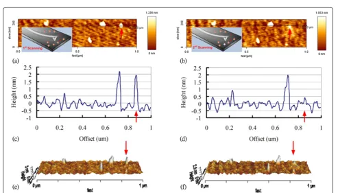
AFM images of a 1.8-nm Au-NP before (first scan) and after (second scan) application of the voltage pulse are presented in Figure 2. The second AFM image con-firms the transfer of the Au-NP following the application of a 2-V pulse for 32 ns.
In approximately half of the experiments, the AFM images do not reveal obvious differences following the application of the voltage pulse (see Additional file 1). This can be attributed to mechanical drift associated with the AFM [17], resulting in the voltage pulse shifting
the position of the selected Au-NP. Another explanation may be that the selected NP was not actually an Au-NP but another nano-object with a height similar to that of the Au-NP.
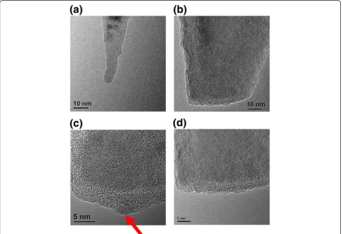
To further verify the attachment of the Au-NP to the probe, we examined TEM micrographs of the modified AFM probe, as shown in Figure 3. To facilitate compari-son, a new probe was also imaged. The original tip radius of curvature was verified as less than 8 nm (Figure 3a). In a series of experiments (using more than 50 AFM probes) and the same voltage pulse of 2 V for 32 ns, we were unable to observe Au-NPs on most of the AFM tips (Figure 3b), suggesting either that the Au atoms were distributed on the AFM tip without any particular structure or that they did not attach. In a few cases, we observed complete Au-NPs on the AFM tips in TEM micrographs; however, these Au-NPs appear to have been adsorbed on the AFM tips randomly [18] (see Additional file 1 for details). We then conducted conjugation experiments using 4-nm QDs to verify the existence of Au on these tips. TEM micrographs demonstrated that 44% of the tips succeeded in picking up single QDs at the vertex (Figure 3c), while the remaining 56% did not (Figure 3d).
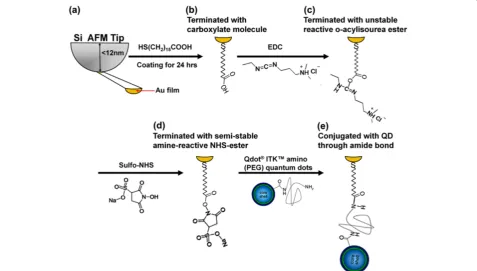
Figure 4 illustrates the process of conjugating the
Au-NP with QDs. HS(CH2)15COOH was first self-assembled
on the Au atoms at the AFM tips to expose the carboxylic
acid functional group (Figure 4a,b) for further QDs conju-gation. Following activation by EDC and sulfo-NHS, an amine-reactive ester formed (Figure 4c,d). Finally,
Qdot® ITK™amino (PEG) QDs conjugated with the
Au-NP through the formation of an amide bond.
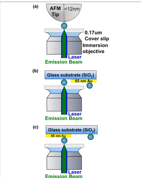
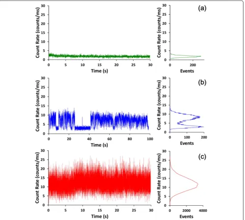
To verify the existence of a single QDs on the AFM tip, we monitored the fluorescence of single QDs using a far-field laser scanning confocal microscope. For com-parison, we prepared half-glass and half-Au film (65 nm) substrates as reference samples (Figure 5). QDs samples were prepared by spin-coating a 0.1-nM solution of QD525 on the glass/Au film (65 nm) substrates. The root-mean-squared (RMS) value of the surface rough-ness on the Au film was estimated at less than 10 nm (see Additional file 1). The resulting emission trajector-ies are presented in Figure 6.
The photoblinking phenomenon, or fluorescence inter-mittency, is an important characteristic of QDs [19]. The term refers to the temporal disappearance of emitted light when molecules or particles undergo reversible transitions between ‘on’ and ‘off’ states. Single QDs on glass clearly demonstrate this phenomenon, leading to bimodal variations in intensity (Figure 6b).
[image:5.595.59.537.419.690.2]This study demonstrated that through the appropriate coupling of Au-NP to the modified AFM probe, single QDs exhibit suppressed blinking and quenched fluorescence
intensity (approximately 2-fold) (Figure 6a). Single QDs on the 65-nm Au film (Figure 6c) also exhibited sup-pressed blinking behavior; however, fluorescence inten-sity was increased (approximately 1.5-fold). Applying QDs on a 10-nm Au film surface resulted in the enhancement of fluorescence intensity approximately 3-fold (see Additional file 1). These results support those of previous studies, in which the intensity of photoluminescence is either enhanced or quenched on roughened and smooth metal surfaces [20-25], respect-ively. However, conjugating QDs to the Au-NP modified-AFM probe presented a slightly different situation, which may be attributed to the effect of the nanoenvironment as-sociated with the QD. These results are similar to those of Ratchford et al. [26] and Bharadwaj and Novotny [27]. In
these studies, an Au-NP was pushed proximal to a CdSe/ ZnS QDs resulting in the quenching of fluorescence inten-sity (approximately 2.5-fold [26] and approximately 20-fold [27], respectively). Our results provide evidence of the existence of a small Au-film on the AFM tip.
Mechanism: evaporation and electromigration
[image:7.595.59.542.89.522.2]One possible mechanism involved in the attachment of a 1.8-nm Au-NP to an AFM tip under a pulse of electrical voltage may be the evaporation and electromigration of Au-NPs induced by the strong electric field, resulting in a small area of Au film coating the AFM tip (an Au film roughly 4 nm in diameter coating the tip without a vis-ible Au particle).
In this scenario, an Au-NP is melted and attracted to the tip apex through a sudden increase in the electric field due to a voltage pulse. Au has a vapor pressure of
10−5 Torr (estimated from bulk Au and is presumably
lower for Au nanoparticles). As a result, Au is first evap-orated and the Au vapor is then guided by the electrical field between the AFM apex and the substrate to be de-posited over a limited region of the AFM apex. The en-ergy required to transfer Au vapor is very small and can be disregarded.
Throughout the Au-NP evaporation process, the en-ergy supplied to the system can be estimated as i0Vst. According to the experimental setup and measurements (see Additional file 1), the values ofi0,Vs, andtwere 3 × 10⁻⁶A, 2-V, and 32 ns, respectively. Equation 1 derives input energyEi:
Ei¼i0Vst¼410−14J: ð1Þ
The minimum required energy Em is that required to
melt the Au-NP and heat the Si tip to the melting temperature of Au. The thermal energy required to melt the Au-NP is mAu-NP CP,Au (Tm,Au-NP–T0), wherem
Au-NPis the mass of the 1.8-nm Au-NP,CP,Au≈129 J/(kgK) is the specific heat capacity of Au,Tm,Au-NP is the
melt-ing temperature of the 1.8-nm Au-NP, andT0≈298 K is
the room temperature [28].
To calculate the mass of Au, we estimated the number of Au atoms in a nanoparticle. Cortie and Lingen [29] pointed out that the atomic packing density of nanogold is approximately 0.70 (between bcc and fcc). There are
about 171 Au atoms in a 1.8-nm Au-NP and mAu-NP=
2.14 × 10⁻²⁷kg (ρAu-NP≈ρAu= 19,300 kg/m3).
Experimental, theoretical, and computer-simulated studies have shown that melting temperature depends on cluster size [29]. These studies suggest a relationship of temperature dependence defined by the following:
Tm=Tb – c / R [30], where Tm is the melting
tempe-rature of a spherical nanoparticle of radiusR,Tbis the bulk melting temperature, andcis a constant. From the literature, Tm,Au-NP≈653 K. Thus, mAu-NP CP,Au (Tm,Au-NP – T0) = 9.8 × 10⁻²³J.
The thermal energy required to heat the apex of the tip to Tm,Au-NP is mapex CP,Si (Tm,Au-NP – T0), where mapex is the estimated mass of the spherical Si tip apex and CP,Si≈712 J/kg/K is the specific heat capacity of Si [28]. The mass of the Si probe to be heated is estimated according to its spherical volume with a radius equiva-lent to the curvature of the tip (12 nm). As a result, Vapex= 7.24 × 10⁻²⁴m3,ρSi= 2,330 kg/m3, andmapexCP,Si (Tm,Au-NP–T0) = 4.27 × 10⁻¹⁵J.
Assuming an adiabatic system (this process occurs in less than 40 ns; therefore, this assumption is reasonably
accurate), the minimum required energyEmcan be
esti-mated using Equation 2:
Em¼mAu−NPCP;Au Tm;Au−NP–T0
þmapexCP;Si Tm;Au−NP–T0
¼4:2710−15J:
ð2Þ
The minimum required energy (Em, Equation 2) is
roughly 1 order of magnitude lower than that of the sup-plied energy (Ei, Equation 1), suggesting that sufficient input energy exists to melt the Au-NPs. This is a reason-able range and can be adjusted through manipulation of the currenti0,mapex, andmAu-NP.
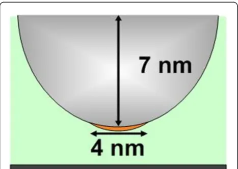
We propose a model of a single-atom layer of Au film formed on the apex of the AFM tip in order to estimate the maximum deposition area by the evaporated Au, as shown in Figure 7. An actual AFM tip image is pre-sented in Figure 3b with no Au-NPs visible on the AFM tip. We estimated that there are roughly 171 Au atoms in a 1.8-nm Au-NP. If these Au atoms were packed closely together, the total area occupied could be
esti-mated as 1,145 Å2(from the 1.46 Å of a single Au atom
radius), resulting in a circle with diameter of approxi-mately 4 nm. This area would be small enough for our prospective single-QDs modification experiment.
[image:8.595.305.539.533.699.2]In Figure 3b, a very small portion of the AFM tip pre-sents a lattice darker than the rest of the Si tip. The tip curvature in this area is greater than that in the new tip. We can deduce from this that Si atoms at the tip surface underwent reflow under the electric field. At the same time, the Au-NP melted, evaporated, and formed a com-pound with the Si at the tip apex. The dark lattice area is estimated to be 1,000 Å2, which is very close to the circular ‘Au-atom-layer’ deposition area (1,145 Å2) pre-dicted by the evaporation, electromigration, and deposition
model. This case represents 44% of all the Au-NP attach-ment cases.
Conclusions
This study presents a novel AFM probe modification scheme in which a 1.8-nm Au-NP is applied by means of a current-limited voltage pulse (2 ~ 5 V,≥32 ns). TEM micrographs and fluorescence inspection results prove the existence of an Au-NP on the apex of the probe. An experiment involving the conjugation of single QDs also demonstrated the existence of a small amount of Au (equal to or less than 4 nm in diameter) deposited on the AFM tips, as well as the ability of the Au-modified AFM tip to pick up single macromolecules (QDs). We also discuss the mechanisms that may be involved in Au attachment: evaporation, electromigration, and depos-ition. The Au-NP was melted, evaporated, and deposited onto the tip apex by a sudden increase in the electric field due to a voltage pulse. The resulting AFM tips present an excellent platform for the manipulation of single protein molecules in the study of single protein-protein interactions.
Additional file
Additional file 1:The file contains the method for the measurement ofI,V, andR; failed experiments; adhesion of an Au-NP to the probe apex during scanning; and experimental setup for fluorescence inspection.
Competing interests
The authors declare that they have no competing interests.
Authors' contributions
FGT conceived of the research work and participated in the analysis. YCC performed the TEM analysis. SNT participated in the bias-applying circuit, coordination, and analysis. CTY and JT performed the fluorescence intensity inspection design and analyses. HWC performed all AFM experiments, analyzed the TEM and fluorescence results, and drafted the manuscript. All authors have read and approved the final manuscript.
Acknowledgements
This work was supported by grants from the National Science Council of Taiwan under the programs no. 102-2627-M-007-002, no. 99-2120-M-007-009, no. 98-2120-M-007-001, no. 98-2627-M-007-002, and no. 98-2627-M-007-001. The authors thank the NTHU ESS TEM Laboratory staff for their help and cooperation. We thank Dr. Tung Hsu at the Department of Material Science and Engineering, National Tsing Hua University, for the generous help with TEM. We also thank Dr. Jin-Sheng Tsi from NSRRC for stimulating discussions and for designing the TEM sample holder.
Author details 1
Department of Engineering and System Science, National Tsing Hua University, 101, Section 2, Kuang-Fu Road, Hsinchu 30013, Taiwan.2Institute of Cellular and Organismic Biology, Academia Sinica, Taipei 11529, Taiwan. 3Medical Image Technology Department, Industrial Technology Research Institute, 195, Section 4, Chung Hsing Road, Hsinchu 31040, Taiwan. 4Department of Physics, Chung Yuan Christian University, Chungli 32023, Taiwan.5Research Center for Applied Sciences, Academia Sinica, 128, Section 2, Academia Road, Taipei 11529, Taiwan.
Received: 17 September 2013 Accepted: 7 November 2013 Published: 15 November 2013
References
1. Binnig G, Rohrer H, Gerber C, Weibel E:Surface studies by scanning tunneling microscopy.Phys Rev Lett1982,49:57–61.
2. Binnig G, Quate CF, Gerber C:Atomic force microscope.Phys Rev Lett1986, 56:930–933.
3. Xie XN, Chung HJ, Sow CH, Wee ATS:Nanoscale materials patterning and engineering by atomic force microscopy nanolithography.Mater Sci Eng R2006,54:1–48.
4. Gan Y:Invited review article: a review of techniques for attaching micro-and nanoparticles to a probe's tip for surface force micro-and near-field optical measurements.Rev Sci Instrum2007,78:081101/1–081101/8.
5. Ducker WA, Senden TJ, Pashley RM:Measurement of forces in liquids using a force microscope.Langmuir1992,8:1831–1836.
6. Ducker WA, Senden TJ, Pashley RM:Direct measurement of colloidal forces using an atomic force microscope.Nature1991,353:239–241. 7. Mak LH, Knoll M, Weiner D, Gorschluter A, Schirmeisen A, Fuchs H:
Reproducible attachment of micrometer sized particles to atomic force microscopy cantilevers.Rev Sci Instrum2006,
77:0461041/1–0461041/3.
8. Lantz MA, Jarvis SP, Tokumoto H:High resolution eddy current microscopy.Appl Phys Lett2001,78:383–385.
9. Berdyyeva TK, Woodworth CD, Sokolov I:Human epithelial cells increase their rigidity with ageing in vitro: direct measurements.Phys Med Biol 2005,50:81–92.
10. Clark SC, Walz JY, Ducker WA:Atomic force microscopy colloid-probe measurements with explicit measurement of particle-solid separation. Langmuir2004,20:7616–7622.
11. Ong QK, Sokolov I:Attachment of nanoparticles to the AFM tips for direct measurements of interaction between a single nanoparticle and surfaces.J Colloid Interface Sci2007,310:385–390.
12. Vakarelski IU, Brown SC, Moudgil BM:Nanoparticle-terminated scanning probe microscopy tips and surface samples.Adv Powder Technol2007, 18:605–614.
13. Vakarelski IU, Higashitani K:Single-nanoparticle-terminated tips for scanning probe microscopy.Langmuir2006,22:2931–2934. 14. Wang HT, Tian T, Zhang Y, Pan ZQ, Wang Y, Xiao ZD:Sequential
electrochemical oxidation and site-selective growth of nanoparticles onto AFM probes.Langmuir2008,24:8918–8922.
15. Okamoto T, Yamaguchi I:Photocatalytic deposition of a gold nanoparticle onto the top of a SiN cantilever tip.J Microsc2001,202:100–103. 16. Hoshino K, Turner TC, Kim S, Gopal A, Zhang XJ:Single molecular
stamping of a sub-10-nm colloidal quantum dot array.Langmuir2008, 24:13804–13808.
17. Schäffer TE:High-speed atomic force microscopy of biomolecules. In Motion in Force Microscopy: Applications in Biology and Medicine.Edited by Bhanu PJ, Heinrich Hörber JK. Hoboken: Wiley; 2006:221–247.
18. Xu J, Kwak KJ, Lee JL, Agarwal G:Lifting and sorting of charged Au nanoparticles by electrostatic forces in atomic force microscopy.Small 2010,6:2105–2108.
19. Yeow EKL, Melnikov SM, Bell TDM, Schryver FCD, Hofkens J:Characterizing the fluorescence intermittency and photobleaching kinetics of dye molecules immobilized on a glass surface.J Phys Chem A2006,110:1726–1734. 20. Ito Y, Matsuda K, Kanemitu Y:Mechanism of photoluminescence
enhancement in single semiconductor nanocrystals on metal surfaces. Phys Rev B2007,75:033309/1–033309/4.
21. Fu Y, Zhang J, Lakowicz JR:Suppressed blinking in single quantum dots (QDs) immobilized near silver island films (SIFs).Chem Phys Lett2007, 447:96–100.
22. Yuan CT, Yu P, Tang J:Blinking suppression of colloidal CdSe/ZnS quantum dots by coupling to silver nanoprisms.Appl Phys Lett2009, 94:243108/1–243108/3.
23. Fujiwara H, Ohtaa H, Chibaa T, Sasakia K:Temporal response analysis of trap states of single CdSe/ZnS quantum dots on a thin metal substrate. J Photochem Photobio A2011,221:160–163.
25. Matsumoto Y, Kanemoto R, Itoh T, Nakanishi S, Ishikawa M, Biju V: Photoluminescence quenching and intensity fluctuations of CdSe–ZnS quantum dots on an Ag nanoparticle film.J Phys Chem C2007,112:1345–1350. 26. Ratchford D, Shafiei F, Kim S, Gray SK, Li XQ:Manipulating coupling
between a single semiconductor quantum dot and single gold nanoparticle.Nano Lett2011,11:1049–1054.
27. Bharadwaj P, Novotny L:Robustness of quantum dot power-law blinking. Nano Lett2011,11:2137–2141.
28. Lide DR:Handbook of Chemistry and Physics.Boca Raton: CRC Press; 2008. 29. Cortie MB, Lingen EVD:Catalytic gold nano-particles.Mater Forum2002,
26:1–14.
30. Bilalbegovic G:Structures and melting in infinite gold nanowires.Solid State Commun2000,115:73–76.
doi:10.1186/1556-276X-8-482
Cite this article as:Chenget al.:Characterization of single 1.8-nm Au nanoparticle attachments on AFM tips for single sub-4-nm object pickup.Nanoscale Research Letters20138:482.
Submit your manuscript to a
journal and benefi t from:
7Convenient online submission
7Rigorous peer review
7Immediate publication on acceptance
7Open access: articles freely available online
7High visibility within the fi eld
7Retaining the copyright to your article