FULL ON
-
CHIP CMOS LOW DROPOUT VOLTAGE
REGULATOR WITH
-
41 dB AT 1 MHZ FOR WIRELESS
APPLICATIONS
1ZARED KAMAL, 2QJIDAA HASSAN, 3ZOUAK MOHCINE
1, 3
Faculty of Sciences and Technology, Electrical Engineering DepartmentFez, Morocco
2Faculty of Sciences Dhar El-Mehraz, Department of Physics, Fez, Morocco
1
[email protected], [email protected], [email protected]
ABSTRACT
A high PSRR full on-chip and area efficient low dropout voltage regulator (LDO), exploiting the nested miller compensation technique with active capacitor (NMCAC) to eliminate the external capacitor and improve the high performance. A novel technique is used to boost the important characteristic for wireless applications regulators PSRR. The idea is applied to stabilize the Low dropout regulator. The proposed regulator LDO works with a supply voltage as low as 1.8 V and provides a load current of 50 mA with a dropout voltage of 200 mV, the PSR of LDO is -60 dB at a frequency of 60 KHz and -41dB at a frequency of 1 MHz. It is designed in 0.18 µm CMOS technology and the active area on chip measures 0.043 mm2. Keyword: Low Dropout Regulator (LDO); MOSCAP; NMCAC; Active Feedback; High PSR; System On
Chip.
1. INTRODUCTION
In the last generation of power management system a switching power converter (SWPC) is followed by a Low Drop-out (LDO) voltage regulator to increasing battery life of portables applications, suppress the ripples at output of the SWPC and provide a clean voltage supply at its output. Due to the increase in operating frequencies, high switching frequencies in SWPC are required for fast transient response in addition to allowing for the use of smaller passive components to reduce area and coast. In the other words, the LDO should have a high Power supply rejection (PSR) up to these few MHz frequencies [1], [8].
Different techniques have been reported to implement LDOs with high PSR at low frequencies. Cascading two pass transistors using drain extended FET transistors [2], and using a voltage subtractor stage with a diode-connected transistor driving the gate of the pass transistor [3] were among the techniques used. Reference [4] was the first to achieve high PSR up to 10MHz frequency through using a cascade of NMOS and PMOS transistors together with a charge pump to bias the NMOS transistor. However, the circuit maximum load current was only 5mA with large drop-out voltage (0.6V). That is in addition to the added complexity
and power consumption of the charge pump. A feed-forward ripple cancellation technique was used in [5], [1] to achieve better PSR up to 10MHz. This technique has a limitation on load current to be only 25mA for good PSR due to having a fixed gain of the feed-forward ripple cancellation path that relies on the ratio of resistors. This ratio can be designed to provide the required cancellation over a narrow load current range.
In this paper, we present a modified NMC with a NMOS source follower stage at PMOS transistor gate to charge rapidly the gate power PMOS capacitance and improve high PSRR. The CMOS capacitor (MOSCAP) is used as a miller capacitor instead of MIMs capacitors or MOM capacitors to reduce the area occupied by the Miller capacitance without influencing stability and realize the full on-chip capacitor LDO with a high performance.
2. PROPOSED LDO
The proposed LDO, shown in Figure 1(a), is composed of two gain stages, a power PMOS transistor and the feedback resistor network. The first stage is the error amplifier (EA). The second is a NMOS gain stage. Cm1, Cm2 are the on-chip active MOS capacitances. Rf1 and Rf2 construct the active feedback resistive network. RL and CL model the equivalent load resistance and load capacitance at the output of LDO. CL is the interconnection lines parasitic capacitor, and typically up to 100 pF. The n-well resistor has a high value for its voltage coefficient, which affect the accuracy in the ICs [6]. Weak inversion region MOS transistors are used as a feedback network resistor instead of conventional n-well resistors in order to lowers quiescent current and save silicon area.
3. ERROR AMPLIFIER
The design of error amplifier (EA) is more complex, when a high performance is required to guarantee the stability and transient response, a specific topology is necessary. To move the dominant pole at the output of E.A to low frequencies, low output impedance is designed. To charge rapidly the capacitance seen at the gate of pass transistor (may be as large as 50 pF), EA must provide a sufficient output current [2], [12]. On the contrary, the EA itself should provide very low power dissipation, and its bias currents must be kept as low as possible. In this paper, the proposed EA is the folded cascode amplifier which offers better performances such as high gain, enough load current to drive the power transistor PMOS and improved PSRR characteristic of LDO.
3.1 MOSCAP Compensation Network
In the full on-chip LDO, the load capacitor modelled at drain of pass transistor is determined by the interconnection lines and typically up to 100 pF. This capacitive value is too small to set a dominant pole at the output node of on-chip LDO [13], [7]. Therefore, the compensation must be achieved through the miller effect. In [14], the
Miller compensation technique is applied to compensate a two-stage Op Amp. As a result, the dominant pole is placed at the output of first stage and moved to low frequencies. The second pole is moved away from the origin of the complex frequency plane. Due to the feedforward path through the Miller capacitor, an undesirable zero occurs on the positive real axis of the complex frequency plane. These approaches require a large compensation capacitor and a high gain of second stage to ensure stability. Moreover, it is difficult to integrate a large capacitor on-chip LDO.
In the recent design of the system on-chip applications, a capacitor MOSCAP was used instead of the MIM or MOM capacitor in Miller compensation. The problem with exploiting MOSCAPs in analog applications is due to the linearity issues [6].This is because of different regions a MOSFET experiences when its gate-bulk voltage varies.
In the proposed structure, the gate-bulk voltage of MOSCAP is controlled and determined by the designer as demonstrated in eq. (2). The MOSCAP is working in the accumulation region, where the capacitance is not dependent on the gate bulk voltage.
The DC potential at the gate and bulk of MOSCAP Cm1 are given by
Vେ୫ଵλଵొ మ భ
ஒభర
ஒర 1
Vୠେ୫ଵ V୭୳୲
Vୠେ୫ଵλଵొ
మ భ
ஒభర
ஒర 1 V୭୳୲ (1)
For keeping the value of capacitor Cm2
independent to its gate- bulk voltage, the following condition must be respected by the designer
λେ୫ଵV୭୳୲ V 2 ∗మ భ
ஒభర
ஒర 1 (2)
Same as in eq. (2), the gate-bulk voltage of compensation capacitor Cm2 is controlled by the
following condition
λେ୫ଶV୭ V 2 ∗య
మ
ஒభర
ஒభభ 1 (3)
Where B1, B2 and B3 are the current gain of current mirrors M4-M14, M17 and M16-M18 respectively and β4, β11, β12 and β14 are the transconductance parameters of transistors M4, M11, M12 an M14 respectively. Ibias is the start-up current of the circuit. From eq. (2), the gate-bulk voltage is independent of the load in the regulation mode. In the worst case, when Iload increases instantaneously, from eq. (2), the bulk voltage of pass element drops in time or the load capacitor CL
As a result, the current gain of current mirror M4-M14 is decreased and the gate voltage of MOSCAP drops verifying the condition of the gate-bulk voltage Vgbcm1 >0.74V as given in eq. (2).
3.2 Stability Analysis
The compensation technique used in this structure places the dominant pole at low frequencies and moves the parasitic poles to high frequencies. The LHP zero is created by the compensation capacitance and improves the phase
margin in time when the RHP zero is placed at high frequencies. The small signal of the proposed LDO is in Figure 1(b). gmp, gm2, gma and gm13, represent
the transconductance of transistors MP, M2 of error amplifier, the NMOS diode and M13 of source follower respectively. gdsp, gds2, and gds13 represent
the conductance of transistors MP, M2 of error amplifier and M13 of source follower respectively. C1, C2, RO1 and RO2 are the output capacitors and
resistors of EA and source follower stage.
a)
[image:3.612.108.500.244.690.2](b)
Figure 1: Proposed LDO a) schematic of CMOS LDO b) small signal of proposed LDO
Active Feedback Power MOS Transistor
MOSCAP Cm2
MOSCAP Cm1 OLIN
NMOS Gain Stage Folded Cascode EA
Startup Circuit
M20 M19
M15
M12 M18
M14 M16
MB
M9
M7
M5
M3
M10
M6
M4
M13
M11
M1 M2 Cm1
Cm2
Rf2 Rf1
MP
IBIAS
OLOUT OLIN
Ma M8
VBG
Vref
1/gma VC=VAE-VGMP
Vfb VOUT
VGMP VAE
RO2 RO1
gm2Vref
gmpVgsp Cm2
Cm1
¡
C2 C1
Rf1
Rf2 CL
rdsp
RL
Assuming that gma<<gmp, and Cm1, Cm2
and CL>>CI, CEA, the small signal loop gain is
given by.
Ts T0 ∗ ൫ଵାୠభୗାୠమୗమ൯
൬ଵାቀୗ ୮ൗ షయౚాቁ൰ሺଵାୟభୗାୟమୗ
మሻ (4)
With T0
g୫ଶg୫ଵଷg୫୮RଵRଶR୭୳୲RଵRଵ Rଶ (5)
Where the dominant pole is at
pିଷୢୠౣమౣ౦ୖోభଵୖోమୖ౫౪େౣభ (6)
And
bଵେౣౣమ, bଶ େౣమౣభେౣ౦ౣమ, aଵ RC
C୫ଶౣమଵ ౣଵ , aଶେౣమౣమେౣ౦ై (7)
Assuming that gma is small and the
non-dominant poles are widely spaced, then the roots of the second-order polynomial in the denominator in eq. (4) are rewritten as
P୬ୢଵ 1
RC C୫ଶ 1g୫ଶ 1g୫ୟ
,
P୬ୢଶେౣ౦ౣమ (8)
In the NMCAC LDO, the dominant pole is unchanged, but the non-dominant poles are pushed to high frequencies. From the polynomial in the numerator of eq. (4) and assuming that the approximation in eq. (7) the two zero are expressed as
Zୌ େౣౣమ,
Zୖୌౣౣమେౣ౦ౣభେౣ౦ౣభ (9) Increasing the load current, the RHP zero and non-dominant pole formed at the output of LDO move to higher frequencies, while the LHP zero is independent of the load current and moved to high frequencies by increasing the current in the NMOS gate stage. From Eq. (7, 9), the damping factor is derived as
ςଵଶRC C୫ଶଵ
ౣమ
ଵ
ౣ
ౣమౣ౦
େౣమେై (10)
In the NMCACR LDO, a small gma
enhances the damping factor without influencing the dc loop gain and without increasing Cm2. the
damping factor is controlled by gma instead of gm2.
From eq. (9) with (W/L)a=5, the ZLHP is placed at
11MHz as presented in fig. 4.
3.3 Power Supply Rejection
The main concept of achieving a better PSR for an LDO relies on providing a path for the ripples appearing at the input of the LDO to be replicated at the gate of the pass transistor. The most literature focuses in its analytic of the PSRR on parameters and devices transmit and control the ripple from the supply to the output of the system neglecting the effect of the parasitic capacitances at the output of error amplifier and its high output stage gain. In this work, a diode Ma is connected at
gate of the pass transistor to control damping factor and enhancing PSR.
The small signal model of PSRR is shown in figure 2. A small signal input voltage vdd will induce an
output voltage vout. The PSRR can be seen to be
PSRR ௩ೠ
௩
൫ౣ౦ିౚ౩౦൯൫౦ାୗେ౦൯ି൫ౚ౩౦ାୗେౙ൯൫ౚ౩భయାୗେౝ౩౦൯
ୟబሺଵାୟభୗభାୟమୗమାୟయୗయሻ
(11)
Where
A୮ g୫ଵଷ gୢୱଵଷ g୫ୟ1 Aୡଶ ,
C୮ Cୱଵଷ Cୱ୮ Cୢ୮,
Cୡ AୡଶC୫ଶ Cୢ୮,
Aୡଶଵା୰୰ౚ౩భభౚ౩భభౣౣ (12)
Assuming that AEA>>RL, gm13, the dc gain of
PSRR can be expressed as
PSRR|ୈେ൫ౣ౦ିౣ౦ౚ౩౦൯ుఽ౦ିౣభయౚ౩౦ౚ౩భయ(13)
As can be seen from eq. (13), the dc gain of PSRR is controlled by the NMOS gain stage performance. At low frequency, in low load condition, gmp decreases, and also the gain of EA
[image:4.612.324.512.548.668.2]decreases.
Figure 2: Small signal model of enhanced PSRR.
From eq. (13), gmp in numerator and
denominator hence PSRR|DC is not heavily affected
by the transconductance variation of power
transistor and is controlled by the gain of M13 and Ma. At full load condition, an increase in gmp and
gain of EA, enhance the PSRR|DC.
In case of having the gate of MP transistor connected to the output of the EA without the NMOS gain stage as in [21]; PSRR|DC can be
expressed as:
PSRR|ୈୈౣ౦ై (14)
As the load current decreases, also the transconductance of MP decreases, the gain of PSRR and the performance of LDO is affected.
From eq. (11), the PSRR drops at two breakpoints Z1 and Z2. Assuming that Z1<<Z2,
gds13<<gmp, Cp is about 24 pF and Cc is about 15 pF,
at moderate frequency, the degradation gain of PSRR is starting at breakpoint zero (Z1) and given
by:
Zଵ େ౦౦ (14)
And
Zଶౣ౦େ౦ିౚ౩భయେౙେౝ౩౦େౙିౚ౩౦େౝ౩౦ (15)
From eq. (14), the first break point Z1 at
moderate frequency is not influenced by different load conditions and can be pushed to high frequency by increasing the transconductance of transistor M13
Ma, or decreasing the gain of divider NMOS
Ma-M11 at gate Power PMOS transistor. As can be seen from eq. (15), the negative time constant formed by Cm2 and Cgsp is subtracted from the time
of the second zero. Consequently, the second zero moves to higher frequencies resulting in higher roll-off PSRR.
4. SIMULATION RESULTS
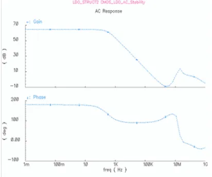
The proposed regulator LDO has been realized in 0.18 µm CMOS technology. The layout of the IC LDO is shown in Fig. 9 with an active chip area of 241 µ m×187 µ m, which is dominated by Power MOS transistor. The on-chip MOS capacitors occupy a small area on chip. The simulation of the proposed LDO was performed with Spectre. The loop-gain simulation has been performed with a total on-chip compensation capacitor Ctotal=24 pF, and the output capacitor CL
(up to 100 pF). The proposed LDO is stable with a good phase margin of approximately 82° at full load as shown in Fig. 4. At low load, the loop’s gain drops to the low value of 39 dB and a phase margin is of 67°.
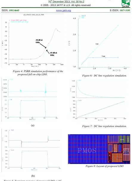
Fig. 5, Shows the simulation of PSRR at 50 mA load current. The impedance inserted at the gate
of power MOS transistor by the NMOS gain stage and transistor Ma enhances the PSRR, and its value
is -61 dB in the range of [0-60KHz]. As depicted in Fig. 5, when a simple NMOS gain stage is inserted at gate of power transistor the PSRR at 1 MHz is about -36 dB and when the novel technique is applied the PSRR at 1MHz is -41.7 dB.
The line regulation simulation of the proposed LDO is shown in Fig. 6. Fig 6(a) shows the AC line regulation for supply voltage change from 2 to 2.5 V. The AC line regulation is about 4 mV with a settling time of 2 µs. Fig 6(b) shows the transient response simulation of the proposed LDO with load current switching between 100 µA and 50 mA. The variation of output is about 110 mV with a settling time of 3 µs for 0.005% accuracy.
[image:5.612.312.518.371.543.2]Another important characteristic of LDO is the DC load regulation as shown in Fig. 8(b), when the load current goes from 0 mA to 50 mA, the variation of the output voltage is 0.6mV/mA. In the worst case (Load current increases from 0 to 50 mA), the output voltage variation is about 67 mV.
Figure 3:Simulation Result Of Proposed LDO
Figure 4: PSRR simulation performance of the proposed full on-chip LDO.
(a)
(b)
Figure 5: Transient response of proposed LDO a) AC line regulation b) AC load regulation.
[image:6.612.85.528.47.653.2]Figure 6: DC line regulation simulation.
[image:6.612.310.523.495.597.2]Figure 7: DC line regulation simulation.
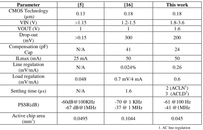
Table 1.Performances and comparison with other works
Parameter [5] [16] This work
CMOS Technology
(µm) 0.13 0.18 0.18
VIN (V) >1.15 1.2-1.5 1.8-3.6
VOUT (V) 1 1 1.6
Drop-out
(mV) >0.15 300 200
Compensation (pF)
Cap N/A 41 24
ILmax (mA) 25 mA 50 50
Line regulation
(mV/mA) N/A 0.024% 0.26
Load regulation
(mV/mA) 0.048 0.7 mV/4 mA 0.6
Settling time (µs) N/A 1.6 2 (ACLN
1)
3 (ACLD2)
PSSR(dB) -60dB@100KHz
-67 dB@1MHz
-70 @ 1 KHz -37 @ 1 MHz
-61 @100 Hz -41 @1MHz
Active chip area
(mm2) 0.0495 0.1044 0.045
1. AC line regulation 2 AC load regulation
5. CONCLUSION
In this paper, a full on chip CMOS LDO using a modified NMC technique has been presented. The regulator circuit design features an active compensation technique, which guarantees the stability through the full load current rage with high PSRR of -60 dB up to 100 KHz and -41 dB at 1MHz. The high performance is independent of the off-chip capacitor. The detailed analysis of the proposed structure is revealed to justify the performance of the technique utilized. The simulations prove the results theory.
The proposed LDO is capable of providing 50 mA with a drop-out voltage of 200 mV at VDD of 1.8 V. The stability is achieved by using the MOSCAP compensation capacitor in the accumulation region. The active area is reduced by 40 % compared to the state-of the-art designs using technologies with the same feature size. The proposed regulator is mainly used as a regulating power source for wireless applications, RFID and charge pumps.
REFERENCES:
[1] G. A. Rincon-Mora, “Active capacitor multiplier in miller-compensated circuits” IEEE
J. Solid-State Circuits, Vol. 35, no. 1, pp. 26-32 Jan. 2000.
[2] S. K. Hoon, S. Chen, F. Maloberti, J. Chen, and B. Aravind, “A low noise, high power supply rejection low dropout regulator for wireless system-onchip applications,” Proc. of IEEE Custom Integrated Circuits Conference, Sept. 2005, pp. 759-762.
[3] W.-J. Huang S.-I. Liu “Capacitor free low dorpout regulators using nested Miller compensation with active resistor and 1-bit programmable capacitor array” IET Circuits
Devices Syst., 2008, Vol. 3, pp. 306-3016.
[4] M. El-Nozahi, A. Amer, J. Torres, K. Entesari, and E. Sánchez-Sinencio, ”A 25mA 0.13µm CMOS LDO regulator with power-supply rejection better than -56dB up to 10MHz using a feedforward ripple-cancellation technique,”
Proc. Of IEEE International Solid-State Circuits Conference, Feb. 2009, pp. 330-331.
[5] A. Amer and E. Sánchez-Sinencio, ”140 mA 90 nm CMSO Low Drop-out Regulator with -56 dB Power Supply Rejection at 10 MHz” IEEE, 978-1-4244-5760-1/10/$26.00©2010.
[6] H. Aminzadeh, R. Lotfi, and K. Mafinezhad “ Area-Efficient Low-Cost Low-Dropout Regulators Using MOS Capacitors” IEEE 1-4244-2542-6/08/$20.00. 2008.
[8] Q. Wu, W. Li, N. Li and J. Ren “A 1.2 V 70 mA Low Drop-out Volyage Regulator in 0.13 µ m CMOS Process” IEEE (2011) 978-1-61284-193-9/11/$26. 00.
[9] K. Zared, H. Qjidaa and M. Zouak, “High PSRR Full On-Chip CMOS Low Dropout Voltage Regulator for Wireless Applications”, IJCA Journal, Vol. 71, No. 18, 2013.
[10]Robert J. Milliken, Jose Silva-Martínez “Full On-Chip CMOS Low-Dropout Voltage Regulator,” IEEE Transactions On Circuits
And Systems—I: Regular Papers, Vol. 54, No.
9, September 2007.
[11]Ma Haifeng, Zhou Feng “Full on-chip and area-efficient CMOS LDO with zero to maximum load stability using adaptative frequency compensation” Journal of Semiconductors, Vol. 31. No. 1 January 2010.
[12]K. N. Leung and P. K. T. Mok, “A capacitor-free CMOS low-dropout regulator with damping-factor-control frequency compensation,” IEEE J. Solid-State Circuits, vol. 37, no. 10, pp. 1691–1701, Oct. 2003. [13]Ch. K. Chava, J. Silva-Martinez, “ A Freqency
Compensation Scheme fo LDO Voltage Regulators” IEEE Transactions on Circuits and
Systems_I: Regular papers, VOL. 51, NO. 6,
June 2004.