Copyright © 2012 IJECCE, All right reserved
Power Optimization on Functional Units of a Generic
Data-path Subsystem
Bantupalli Divakar
(M.Tech.) VLSI System Design, ADITYA INSTITUTE OF TECHNOLOGY ANDMANAGEMEN, TEKKALI, A.P., INDIA E-Mail ID : [email protected]
K V Lalitha Bhavani, M.Tech.
Sr. Asst. ProfessorADITYA INSTITUTE OF TECHNOLOGY AND MANAGEMEN, TEKKALI, A.P. INDIA
E-Mail ID :[email protected]
Abstract
—
Data path is the core of the processor, where all computations are performed. The other blocks in the processor are support units. At present, most of the popular processor hardware synthesis tools give higher priority to delay. So the processor synthesis tools tend to generate data path architecture for faster implementation. With increasing importance of power reduction on a processor, it is becoming necessary to evaluate different data path architectures from the point of view of both delay and power. This work is aimed at characterizing various architectures implementations of common operators for power, delay and area for different algorithms of adders, multipliers, comparators, shifters etc. and selecting a particular low power architecture where delay is not critical. Finally optimizing the data paths for a general purpose processor. Most of power consumption in the processor is due to adders, multipliers, shifters and comparators.Keywords
—
Bypass multipliers, tree multipliers, mixed style multipliers, clock gating.I. I
NTRODUCTIONLow power issues have become an important factor in modern VLSI design, for both environmental reasons as well as to preserve battery life. However, different implementation technologies present different power optimization opportunities. Dynamic power dissipation is the result of charging the load capacitances in a circuit. It is given by equation Pd=CLV2DDE(sw)fclk,where CLis the
output capacitance, VDD the supply voltage, E(sw) is the
average number of transitions and fCLK is the clock
frequency.
In the past, different architectural optimizations have been applied in order to minimize dynamic power dissipation in arithmetic circuits, and especially in digital multipliers [1],[2]. Multipliers are very important devices in DSP applications, like for example FIR filters. Multipliers are much larger than adders and also more power consuming. Multiplication is actually a process of addition of multiple partial products. These partial products are formed by operating the multiplicand by each bit/bits of the multiplier. There are different multiplier architectures formed depending on the method of generation of partial product and its addition to finally give the complete product. The partial products can be computed using the normal ANDing operation or by using some encoding method. Multiplications are expensive and slow operations. In the performance of many computational problems often is dominated by the speed at
which a multiplication operation can be executed. Multipliers are in effect complex adder arrays.
The analysis of the multiplier gives us some further insight into how to optimize the performance of complex circuit topologies. There are different approaches to partial product generation, accumulation and final summation. Clock gating was originally conceived as a system level power optimization technique aiming to reduce the power dissipated on the clock network (which accounts up to 40% of the total)by deactivating parts of the system that are idle. Its applicability has been extended to the RT level as a power efficient implementation of registers on a hold condition. During a hold condition, the register preserves its previous value at a high power cost. Unnecessary power is consumed on the clock line, the register itself and on the multiplexer on the feedback path. By controlling the clock driving the clock input of the register, reloading is only conditionally performed resulting in both reduced power consumption and area overhead.
The two main choices for the design of a multiplier are the tree form, like the Wallace tree, which has the advantage of a logarithmic circuit delay, and the array form, like the Carry-Save array, where the delay is linear [3]. The advantage of the array multiplier is its regular structure, which leads to a dense layout, ideal for fabrication.
II. N
ORMAL ANDB
YPASSM
ULTIPLIERSConventional design of hardware multipliers using the serial-shift and parallel-add techniques are less expensive to implement, especially with micro programmed controls. However, the add-shift approach is still considered too
slow to satisfy today’s scientific and engineering demands
for faster multiplication. Ever since the advents of LSI circuits, high speed cellular array multipliers have been a logical and feasible improvement over the serial-parallel design. Their gains in the speed are obtained at the expense of extra hardware investment.
Consider two unsigned integer A= am-1,...a1,a0 and B= b n-1,……b1,b0with values Avand Bv, respectively,
….. 2.1 …...2.2
In binary multiplication, the (m+n) bit product P=P m+n-1,….P1,P0is formed by multiplying the multiplicand A by
multiplier B. The product P has a value, PV= AvBv=
Copyright © 2012 IJECCE, All right reserved The normal 4X4 carry save array multiplier FA* cell is
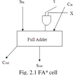
used. The carry save array is a straight forward technique in vector implementation. It consists of partial product reduction tree, which is used to calculate partial product in carry save redundant form and final chain adder to transform the redundant form into normal binary form. The functionality of the carry save array multiplier is as follows. X= (xn-1,…x1,x0) and Y= (yn-1,…y1,y0) are inputs
and these inputs are fed to the array of FA* cells shown in figure 2.1, Each FA* cell performs xi*yj using an AND
gate and then adds the resultant with the incoming carry bits, to produce an output sum and output carry. Here Sin is the incoming sum input, X and Y are multiplier and multiplicand bits, Cin is the incoming carry bit, Sout is the sum output and Cout is the carry output.
Fig. 2.1 FA* cell
This full adder cell is repetitively used in the multipliers operation. Multiplication is nothing but the repetitive addition of partial products. In general the array multipliers give the advantage of dynamic power savings. Due to the large no. of almost identical critical paths, increasing the performance of the structure through transistor sizing yields marginal benefits. A more efficient realization can be obtained by noticing that the multiplication result does not change when the output carry bits are bypassed diagonally downwards instead of only to the right. We include an extra adder called vector merging adder to generate a final result. The resulting multiplier is nothing but carry save multiplier, because carry bits are not immediately added, but rather are saved for the next stage. In the final stage carries and sums are merged in a fast carry propagate adder stage. While this structure has a slightly increased area cost, it has an advantage of that its worst case critical path and are uniquely defined.
All the FA* cells are placed appropriately as shown in the fig 2.2 to perform multiplication. The final adder in the figure is used to merge the sums and carries from the last row of the every array, since in every row the carry bits are not immediately added but rather propagated to the row. There is drawback of the normal multiplier that is uses FA* cell that when Yjis zero the corresponding cells
are functioning unnecessarily. So to block the operation a new cell structure that blocks unwanted diagonal. It uses a new architecture, bypass multiplier.
Mixed style Architecture, was proposed here to minimize the power dissipation in digital multipliers, starting from dynamic power and concentrating on
switching activity. Minimization of switching activity in a digital circuit can be performed by isolating units producing non valuable partial products, in order to save power [4]. The estimation and minimization of switching activity in combinational circuits by considering both transitions, 10 and 01. To minimize the switching activity, eliminating input inverters or increasing the number of inputs to a gate.
Fig.2.2 A 4x4 Carrysave array Multiplier
There have been lot of techniques to reduce the switching activity; the one of the most important technique is that clock gating. To save power, clock gating support adds more logic to a circuit to prune the clock tree, thus disabling portions of the circuitry so that its flip flops do not change state. Their switching power consumption goes to zero and only leakage currents are incurred. Here a new technique in the place of clock gating is used i.e. use of transmission gates [5].
The main drawback of the normal carry save multiplier is that when Y is 0 then the corresponding cells are functioning unnecessarily. If Xi*Yjand carry input is zero
then the sum output is nothing but sum input. Consequently, the sum output of the above cell can bypass the unimportant diagonal with the use of transmission gates. So, FA* cell can be replaced by FAB cell(as shown in figure 2.3) means full adder cell with bypassing technique[6].
The operation of the FAB cell is that X and Y are multiplier and multiplicand bits, Sin and Cin are the sum input and carry input respectively. In figure 2.3 Y is used as control signal. Here the transmission gates are implemented using CMOS gates
Copyright © 2012 IJECCE, All right reserved Fig.2.4 The proposes 4X4 Carry save array multiplier with
bypass
In the FAB cell, if Y=0, the X and Sin inputs are blocked rather than that Sin input is send to the multiplexer and the same way if Y=0 the Sin input is send to the Sout terminal. Suppose if Y=1 then the sum output of the cell is propagated from the full adder. The carry input does not generate any new value since the diagonal carry input is always 0. If Y=0, to fix the erroneous carry generated from previous blocks, an AND gate is used before the final adder to make the final diagonal carry output to 0. This is the modified bypass multiplier that can be used in our mixed style multiplier architecture. Because of this bypassing technique the delay can be reduced with the area overhead. All the FAB cells are placed appropriately as shown in the fig 2.4 to perform multiplication. The final adder in the figure 2.4 is used to merge the sums and carries from the last row of the every array, since in every row the carry bits are not immediately added but rather propagated to the row.
III. W
ALLACET
REEM
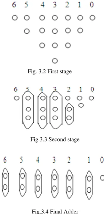
ULTIPLIERSThe partial sum adders can also be rearranged in a tree like fashion, reducing both the critical path and the number of adder cells needed [7]. The number of full adders needed for this operation can be reduced by observing that only column 3 in the array has to add four bits. All other columns are somewhat less complex. The example for tree arrangement is as shown in figure 3.1.
Fig.3.1 Partial products
Fig. 3.2 First stage
Fig.3.3 Second stage
Fig.3.4 Final Adder
Consider a simple example of four partial products each of which is four bits wide, as shown in figure 3.1. In figure 3.2, where the original matrix of partial products is organized into a tree shape to visually illustrate its varying depth. The challenge is to realize the complete matrix with a minimum depth and minimum number of adder elements. The first type of operator that can be used to cover the array is a full adder, which takes three inputs and produces two outputs: the sum, located in the same column and the carry, located in the next one. For this reason, the FA is called 3:2 compressors. It is denoted by a circle covering three bits. The other operator is the half adder, which takes two input bits in a column and produces two outputs. The HA is denoted by a circle covering two bits.
To arrive at the minimal implementation, we iteratively
cover the tree with FA’s and HA’s, starting from its
densest part. In first stage introducing HA in column 4 and 3 as shown in figure 3.2. The reduced tree is as shown in figure 3.3. A second round of reductions creates a tree of depth 2 as shown in figure 3.3. Only three FAs and three HAs in the reduction process, compared with six FAs and six HAs in the carry save multiplier of figure 2.2 and 2.4. The final stage consists of simple two input adder, for which any type of adder can be used.
Copyright © 2012 IJECCE, All right reserved
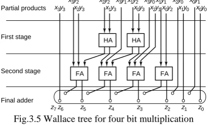
the tree is equal to Ο ( ). While substantially faster than the carry save structure for larger multiplier word lengths, The Wallace tree has the disadvantage of being very irregular, which complicates the task of coming up with dense layout. This irregularity visible even in the four bit implementation
Partial products
First stage
Second stage
Final adder
FA FA FA
HA HA
FA
x3y3
z7z6 z5 z4 z3 z2 z1 z0 x3y2
x2y3
x1y1
x3y0 x2y0 x0y1 x0y2 x2y2
x1y3 x1y2 x3y1
x0y3 x2y1 x1y0 x0y0
Fig.3.5 Wallace tree for four bit multiplication There are numerous other ways to accumulate the partial product tree. A number of compression circuits have been proposed in the literature. They are all based on the concept that when full adders are used as 3:2 compressors, the number of partial products is reduced by two thirds per multiplier stage.
IV. M
IXEDM
ULTIPLIERSIn general, array multipliers offers dynamic power saving but it fails to give a reduced area and fast speed advantages because of their regular interconnection pattern. So, tree multipliers are introduced to achieve reduced area and fast speed. Therefore to achieve both delay and power advantages, it is better to use a different architecture that is having two different parts one is tree based part and other is bypass architecture[5],[8].
Fig.4.1 8 bit multiplication split in parts
The 8x8 Mixed style multiplier shown in fig. 4.1.Two 8-bit values can be multiplied by splitting each one of them in two 4 bit parts. If the first value is (A,B) and the second (C,D), four 8 bit partial products are generated, X=AxD, Y=BxD, Z=AxC and W=BxC. These four partial products shifted and added together generate the final 16-bit result.
In the modified architecture, bypass technique offers minimum dynamic power compared to normal carry save array multiplier and the tree based part offers good performance.
V. R
ESULTS ANDC
ONCLUSIONSPerformance Evaluation:
Table I
Implementation Results of Multiplier Architectures
Copyright © 2012 IJECCE, All right reserved These Multipliers of resolution 8x8, 16x16 and 32x32
were implemented on Xilinx Spartan 3E FPGA. From the table I, it can be observed that, the mixed architecture offers advantages in the reduction of dynamic power, combined with advanced performance (best PDP).The table also shows the performance metric, such as area in terms of LUTs, for all the Multipliers.
VI. C
ONCLUSIONIn this work, I have implemented Multipliers [9] [10] for Low power Applications. For power optimization, two basic algorithms, namely Wallace Tree and Array Multiplier, are combined to exploit the low power and High Performance gains from the individual architectures. This topology, called as mixed style Multiplier was implemented on Spartan 3E FPGA and it was observed that the power dissipation and the critical path delay are fairly lower than the normal multiplier. Power
Measurements were performed using Xilinx “Xpower Analyzer “[11]], for various test cases like counter type and random patterns. It is possible to extend the resolution of the mixed style multiplier, without affecting the performance. Also, this design can be implemented by using standard cell libraries designed for low power, with ASIC Development Kit for improving the performance relatively.
R
EFERENCES[1] M.Karlsson, “A generalized carry-save adder array for digital signal processing”, in 4thNordic Signal Processing Symposium. IEEE, 2000.
[2] P.Meier, R.A.Rutenbar, and L.R. Carley, “Exploring multiplier architecture and layout for low power”, in
Custom Integrated Circuits Conference”. IEEE,1996. [3] N.Weste and D.Harris, CMOS VLSI Design: A circuits
and systems perspective – Third Edition. Addision –
Wesley, 2004
[4] J.Rababey and M.Pedram, Low Power Design
Methodolies. Kluwer Academic Publishers, 1996. [5] Dimitris Bekiaris, George Economakos and Kiamal
Pekmestzi “A mixed style multiplier architecture for low
dynamic and leakage power dissipation”, National
Technical university of athens, School of Electrical and Computer Engineering, 2010.
[6] C.C.Wang and G.N. Sung, “Low-Power multiplier design
using a bypass technique”, Journal of signal processing systems, 2008
[7] Kai Hwang, “Computer Arithmetic, Principles, Architecture and Design”, John Wiley, 1978.
[8] G.Economakos and K. Anagnostopoulos, “Bit level
architectural exploration technique for the design of low power multipliers”, in International Symposium on
circuits and systems. IEEE, 2006.
[9] Advanced digital design with the verilog hdl by Michael D.Clietti.
[10] Verilog HDL, A Guide to Digital Design and Synthesis by samir palnitkar.
[11] Xilinx tool user guide.
A
UTHORSP
ROFILEDivakar Bantupalli
completed my Bachelor degree in the stream of Electronics and Communications Engineering in the year of 2010. Later joined as regular student for Master of Technology in the stream of VLSI SD. My research area is VLSI System design.