8thSASTech 2014Symposium on Advances in Science & Technology-Commission-IV Mashhad, Iran
FPGA Implementation of Interleaver
Morteza Zilaei Bouri
Designation Master Degree, Organization: Islamic Azad University science and research, Khorasan-e-Razavi Branch (Neyshabur), Email ID: [email protected]
Name:Zohreh Mohammadkhani
Designation Master Degree, Organization: Islamic Azad University science and research, Khorasan-e-Razavi Branch (Neyshabur), Email ID: [email protected]
Name: Seyed Reza Talebiyan
Designation: Assistant Professor, Organization: International Imam Reza (AS) university, Email ID: [email protected]
Abstract — Wireless technology, one of the fastest segments of the modern communications industry is growing. The IEEE 802.16e standard as we know by the name mobile Worldwide Interoperability for Microwave Access (WiMAX) commonly, the latest wireless technology is broadband wireless access for over long distances. Orthogonal Frequency Division Multiplexing (OFDM) concept to speed up data transfer and to reduce adverse effects such as interference with the internal display (ISI) and the Input Channel Interference (ICI) is used in OFDM. For next generation air wireless broadband systems plays interface role. In this review Article, we study a method based on finite state machine (FSM) for modeling multimode addressable generator WiMAX interleaver using Very High speed integrated Circuit Hardware Description Language (VHDL) on Field Programmable Gate Array (FPGA) with multi-rate codes and programs for all standard IEEE 802.16e, has been introduced. The proposed method works better at high frequencies, and with minimal loss of logic cells compared with the existing FPGA based approach, uses flip-flops. At the end, interleaver in WiMAX system and modeling of the hardware was studied.
Keyword — FPGA, FSM, Multi-detector, WLAN.
1. I
NTRODUCTIONBroadband Wireless Access (BWA) is the most challenging segment of the wireless revolution since it has demonstrated a viable alternative to the cable modem and digital subscriber line in the last mile access environment [1]. High processing speed, design flexibility and fast design Turn A round Time (TAT) are the important requirements of BWA to meet the challenges poised to it. These requirements make the designers to choose reconfigurable hardware platform like Field Programmable Gate Array (FPGA). A product implemented on FPGA can easily be upgraded by making necessary changes in the Hardware Description Language (HDL) code and thus becomes obsolescence free. In addition, the TAT of FPGA based circuits is
much shorter compared to Application Specific Integrated Circuit (ASIC). A Wireless Local Area Network (WLAN) interconnects two or more communicating devices using some wireless distribution method and usually providing a connection through an access point (AP) [2] to the wider internet. IEEE 802.11a [2] and IEEE 802.11g [3] based WLAN use Orthogonal Frequency Division Multiplexing (OFDM) [2] PHY layer that greatly increases the overall throughput at the AP. OFDM technique is gaining popularity; technique offers promising solution that has gained tremendous research interest in recent years due to its high transmission capability and also for alleviating the adverse effects of Inter Symbol Interference (ISI) and Inter Channel Interference (ICI). In an OFDM system, the data is divided into multiple parallel sub streams at a reduced rate, and each is modulated and transmitted on a separate orthogonal subcarrier. This increases symbol duration and improves system robustness. OFDM is achieved by providing multiplexing on users’ data streams on both uplink and downlink transmissions. OFDM is the fundamental building block of the IEEE 802.16 standard.
2. I
NTERLEAVERInterleaving plays a vital role in improving the performance of Forward Error Correction (FEC) codes in terms of Bit Error Rate (BER). Interleaving is the process to rearrange code symbols so as to spread burst of errors into random like errors and thereafter FEC techniques could be applied to correct them. In popular block interleaver, the bits received from the encoder are stored row wise in the interleaver’s memory and read column wise. WiMAX uses a special type of block interleaver in which the interleaver depth and pattern vary depending on the code rate and modulation type (mod-type). Use of multiplexers to model the various specifications of WiMAX interleaver into a single circuit is an efficient approach leading to multimode interleaver.
8thSASTech 2014Symposium on Advances in Science & Technology-Commission-IV Mashhad, Iran
solution from implementation point of view. A few implementation of interleaver having different specifications are found in the literature. Ahmad Sghaier et al. [3] have described a look up table based method for address generation of the interleaver used in IEEE 802.11 WLAN. Recently Khater et. al. [4] described a using Very High speed integrated Circuit Dardware Description Language (VHDL) based implementation of interleaver Address Generation circuitry for IEEE 802.16e interleaver with ½ code rate. In this paper we propose a novel FSM based, multimode interleaver for OFDM based WLAN. As per IEEE 802.11a and IEEE 802.11g standard, ½, ⅔ and ¾ are the allowed code rates whereas Binary Phase-Shift Keying (BPSK), Quadrature Phase-Shift Keying (QPSK), 16-Quadrature Amplitude Modulation (QAM) and 64-QAM are the permitted modulation schemes and
The principal aim of this work is to present a novel FSM based multimode, high speed and hardware efficient technique to implement the Address Generation circuitry of WiMAX interleaver based on IEEE 802.16e standard on FPGA platform.
IEEE 802.11a and IEEE 802.11g based WLAN uses.
3. I
NTERLEAVING INOFDM
BASEDWLAN
Identical interleaving technique in which a special type of block interleaver is used. the Interleaver depth varies with modulation scheme. The interleaver action can be expressed in terms two sets of equations which ensures the following two design rules:1) The adjacent coded bits are mapped to non-adjacent sub-carriers.
2) Adjacent coded bits are mapped alternatively to less and more significant bits of the constellation to avoid long run of lowly reliable bits.
Let Ncbps is the block size corresponding to the number of coded bits per allocated sub-channels per OFDM; d represents number of columns of the block interleaver which is typically chosen to be 16. mk is the output after first level of permutation and k varies from 0 to Ncbps -1. S is a parameter defined as s=max {1, Ncpc/2}, where Ncpc is the number of coded bits per sub-carrier as shown in Table (1).
Mk = ( )(k%d) + (1)
Jk = sx + (mk + Ncbps - ) %s (2)
Where % and ⎣ ⎦ signify modulo and floor functions respectively.
Table (1)Specifications OF IEEE 802.11a and IEEE 802.11g based WLAN Interleaver.
Modulation Scheme
Ncpc S Ncbps NO. of Rows in
interleaver memory
BPSK 1 1 48 3
QPSK 2 1 96 6
16-QAM 4 2 192 12
64-QAM 6 3 288 18
3.1. Hardware model of interleaver
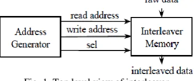
The proposed hardware model of OFDM based WLAN interleaver consists of two sections: address generator and interleaver memory as shown in Fig. 1. The address generator is basically the simultaneous implementation was calculated by using (1) and (2) which is the write address along with provision for generation of read address for interleaver memory. Block interleaver uses two memory blocks out of which one memory block is written and the other is read based on the value of select (sel) signal.
A. Address generator
Table (2) lists first 32 write addresses of the interleaver for all four mod-type obtained by evaluating (1) and (2). Careful examination of the write addresses reveals that the subsequent addresses are not equally spaced for all the cases. Within a particular modulation scheme, the increment values follow a fixed type of pattern. In case of BPSK and QPSK (with s = 1) the increments are linear having value 3 and 6 respectively. 16-QAM and 64-QAM have nonlinear increments e.g., 13, 11 and 20, 17, 17 respectively.
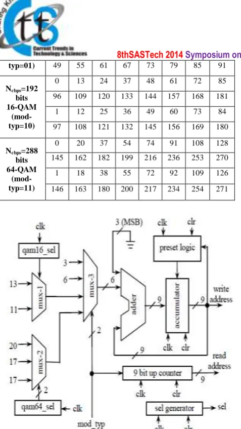
Our proposed design of address generator block is described in the form of schematic diagram in Fig. 2. Bulk of the circuitry is used for generation of write address. It contains three multiplexers: mux-1 and mux-2 implements the unequal increments required in 16-QAM and 64-QAM whereas mux-3 routes the outputs received from mux-1 and mux-2 along with equal increments of BPSK and QPSK. The select (sel) input of mux-1 is driven by a T-flipflop named qam16_sel whereas that of mux-2 is controlled by a mod-3 counter, qam64_sel. The two lines of mod-typ are used as sel input of mux-3. The 6-bit output from the mux-3 acts as one input of the 9-bit adder after zero padding. The other input of the adder comes from accumulator, which holds the previous address. After addition a new address is written in the accumulator.
Fig. 1. Top level view of interleaver
Table (2) First 32-write addresses for four modulations Schemes and their encoding
Ncbps=48bi ts BPSK (mod-typ=00)
0 3 6 9 12 15 18 21
24 27 30 33 36 39 42 45
1 4 7 7 13 16 19 22
25 31 31 31 37 40 43 46
Ncbps=96 bits QPSK
8thSASTech 2014Symposium on Advances in Science & Technology-Commission-IV Mashhad, Iran typ=01) 49 55 61 67 73 79 85 91
Ncbps=192 bits 16-QAM
(mod-typ=10)
0 13 24 37 48 61 72 85 96 109 120 133 144 157 168 181 1 12 25 36 49 60 73 84 97 108 121 132 145 156 169 180
Ncbps=288 bits 64-QAM
(mod-typ=11)
0 20 37 54 74 91 108 128 145 162 182 199 216 236 253 270 1 18 38 55 72 92 109 126 146 163 180 200 217 234 254 271
Fig. 2. Schematic diagram of address generator
The preset logic is a hierarchical FSM whose principal function is to generate the correct beginning addresses for all subsequent iterations and is shown in the form of state diagram in Fig. 3. This block contains a 4-bit counter keeping track of end of states during the iteration. The FSM enters into the first state with CLR=1. Based on the value in mod-typ it makes transition to one of the four possible next states (SMT0, SMT1, SMT2 or SMT3). Each state in this level represents one of the possible modulation schemes. The FSM thereafter makes transition to the next level of states (e.g., S000, S001 and so on) based on the value in the accumulator. When the FSM at this level reaches to the terminal value of that iteration (e.g., 45 in SMT0), it makes transition to a state (e.g., S000) in which it loads the accumulator with the initial value (e.g., preset=1) of the next iteration. This process continues till all the interleaver addresses are generated for the selected mod-typ. If no changes take place in the values of mod-typ, the FSM will follow the same route of transition and the same set of interleaver addresses will be continually be generated. Any change in mod-typ value causes the interleaver to follow a different path. In order to facilitate the address generator with on the fly address computation feature, we have
made the circuit to respond to CLR input followed by mod-typ inputs at any stage of the FSM. With CLR=1 it comes back to SF state irrespective of its current position and there after transits to the desired states in response of new value in mod-typ.
Fig. 3. State diagram of preset logic
The read addresses are linear in nature and are generated using a nine bit up counter as shown in Fig. 2. The counter is reset whenever it reaches to the terminal count for a desired modulation scheme. For example, in case of 16-QAM, the counter counts from 0 to 191 and then repeats. The sel generator is basically a T- flipflop used to generate the sel signal and is initialized to zero using CLR input.
B. Interleaver memory
The interleaver memory block comprises of two memory modules (RAM-1 and RAM-2), three muxs and an inverter as shown in Fig. 4. In block interleaving when one memory block is being written the other one is read and vice-versa. Each memory module receives either write address or read address with the help of the mux connected to their address inputs (A) and sel line. RAM-1 at the beginning receives the read address and RAM-2 gets the write address with write enable signal of RAM-2 active. After a particular memory block is read / written up to the desired location, the status of sel changes and the operation is reversed [5]. The mux at the output of the memory modules routes the interleaved data stream from the read memory block to the output.
C. Modeling memory in FPGA
8thSASTech 2014Symposium on Advances in Science & Technology-Commission-IV Mashhad, Iran
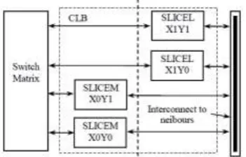
5. The two LCs of a SLICEM slice can be utilized as two 16 X 1 bit DRAM. The LCs of slice, SLICEL can be used as ROM/logic generator. Each 16 X 1 RAM can be cascaded for deeper and wider memory applications. Spartan- 3, Device XC3S400 FPGA offers 56Kbits of DRAM.
Fig. 4. Schematic view of Interleaver Memory block
Fig. 5. Internal structure of a CLB in Spartan 3 FPGA
Bits of dedicated BRAM arranged in 16 blocks of 18K bit each. Out of 18K bits, 16K bits are used for data and rest 2K bits are used for parity purpose. Each block can be organized in various manner like 16K X 1bit, 8K X 2bit, 4K X 4bit etc. The maximum memory required for OFDM based WLAN interleaver is 288 bits. Two identical memory blocks each of capacity 288 bits are required for implementation of block interleaver. To model this memory in FPGA we have followed two techniques: one using DRAM and the other using BRAM. To model 288 bits memory we require four 64 X 1bit and one 32 X 1bit DRAM as shown in Fig. 6. The write enable logic is designed with the help a 3 to 5 decoder as shown Fig. 7. Table (3) shows the conditions in which the WE signals for various DRAM blocks are generated. Modeling the interleaver memory using BRAM is relatively simpler than DRAM approach. BRAM of 16K X 1 bit has been utilized to model the memory.
Table (3) First 32-permutation sample addresses for three code rates and modulation schemes
Ncbps=96
Bits, 1/2
0 6 12 18 24 30 36 42 48 54 60 66 72 78 84 90
Code rate QPSK
1 7 13 19 25 31 37 43 49 55 61 67 73 79 85 91 Ncbps=288
Bits, 3/4 Code rate 16-QAM
0 19 36 55 72 91 108 127 144 163 180 199 216 235 252 271 1 18 37 54 73 90 109 126 145 162 181 198 217 234 253 270 Ncbps=384
Bits, 2/3 Code rate 64-QAM
0 26 49 72 98 121 144 170 193 216 242 265 288 314 337 360 1 24 50 73 96 122 145 168 194 217 240 266 289 312 338 361
6. I
NTERLEAVING INWLAN
6.1.System descriptionThe system level overview of IEEE 802.16e based WiMAX system is described in Fig.1. In this system, the input binary data stream obtained from a source is randomized to prevent a long sequence of 1s and 0s, which will cause timing recovery problem at the receiver. The randomized data bits are thereafter encoded using Reed Solomon (RS) encoder followed by Convolutional Coder (CC). The former is suitable for correction of burst type of errors whereas the latter is for random errors. After RS-CC encoding, all encoded data bits are to be interleaved by a special type of block interleaver. In the block interleaver of WiMAX system, data is written sequentially in the memory and read in a random manner based on certain permutation [9].
Thereafter data passes through the mapper block in which modulation takes place. The resulting data symbols are used to construct one OFDM symbol by performing Inverse Fast Fourier Transform (IFFT). Cyclic Prefix is used to reduce ISI and ICI. The receiver section as shown in Fig.1 works exactly in reverse order.
Fig. 6. Overview of WiMAX PHY Layer system
4.2.Gardware modeling of address generator for wimax interleaver
8thSASTech 2014Symposium on Advances in Science & Technology-Commission-IV Mashhad, Iran
and increment values from implementation point of view are presented in Table (4)
The Address Generation concept of the proposed block interleaver is described in the form of schematic diagram as shown in Fig. 2. Unlike [8], our design includes all possible code rates and mod-type permitted under IEEE 802.16e. As shown in Fig. 2, the design concept contains three levels of multiplexer (MUX). The first level MUXs implement the unequal increments required in 16-QAM and 64-QAM. The four-interleaver depths of 16-QAM as shown in Table (4) are implemented by the first four MUXs from the top in level 1. The sel inputs of these four MUXs are tied together and are driven by a T-flipflop named QAM16_SEL. Similarly, the last four MUXs are for 64- QAM modulation. The sel inputs are driven by a mod-3 counter - QAM64_SEL. The second level MUXs basically pick up one inputs based on the values of ID. The topmost MUX in level 2 implements the eight interleaver depths of QPSK modulation scheme available by concatenation of sub-channels [10]. The second and third MUXs in level 2 are for 16-QAM and 64-QAM respectively. The outputs from level 2 MUXs are routed to the next section by level 3 MUX based on mod-type value. The 7-bit output from the level 3 MUX acts as one input to the 10-bit adder circuit after zero padding. The other input of the adder comes from Accumulator, which holds the previous address. After addition a new address is written in the Accumulator. The preset logic is a FSM whose principal function is to generate the correct beginning addresses for all subsequent iterations and is described at length in the next section.
4.3. Preset logic as finite state machine
The Preset Logic block of Fig. 2 is the heart of the Address Generator of WiMAX interleaver. It is basically a hierarchical FSM and the state diagram is shown in Fig. 3. This block contains a 4 bit counter keeping the track of end states during the iteration. The FSM enters into the first state with CLR=1. Based on the value in mod-type it makes transition to one of the three possible next states (SMT0, SMT1 or SMT2). Each state in this level
Table (4) Increment values for various interleaver depths and modulation schemes with their encoding
M o d u la ti o n M o d -t y p e In te rl e a v e r D e p th ID In te rl e a v e r V a lu e We th e r e q u a ll y sp a c e d
QPSK 0 96 000 6 Yes
144 001 9 Yes
192 010 12 Yes
288 011 18 Yes
384 100 24 Yes
432 101 27 Yes
480 110 30 Yes
576 111 36 Yes
16-QAM 01 192 X00 1311 No
288 X01 1917 No
384 X10 2523 No
576 X11 3735 No
64-QAM 1X 288 X00 201717 No 384 X01 262323 No 432 X10 292626 No 576 X11 383535 No
represents one of the possible modulation schemes. The FSM thereafter makes transition to one of the next level states (SID0 to SID7 from SMT0, SID0 to SID3 from SMT1 or SMT2) based on the value in ID. The various states of this level signify one of the interleaver depths. From these states it branches to next level of states based on the value in the accumulator.
When the FSM at this level reaches to the terminal value of that iteration (e.g., 90 in SID0 of SMT0), it makes transition to a state (e.g., S000) in which it loads the accumulator with the initial value (e.g., Preset=1) of the next iteration. This process continues till all the interleaver addresses are generated for the selected ID and mod-type. If no changes take place in the values of ID and mod-type, the FSM will follow the same route of transition and the same set of interleaver addresses will be continually be generated. Any change in ID and mod-type value causes the interleaver to follow a different path. In order to facilitate the Address Generator with on the fly address computation feature, we have made the circuit to respond to CLR followed by ID and mod-type inputs at any stage of the FSM. With CLR=1 it comes back to SF state irrespective of its current position and there after transits to desired states in response of new values in ID and mod-type.
9. C
ONCLUSION8thSASTech 2014Symposium on Advances in Science & Technology-Commission-IV Mashhad, Iran
R
EFERENCE[1] Konhäuser W, “Broadband Wireless Access Solutions-Progressive Challenges and Potential Valueof Next Generation Mobile Networks”, Wireless Personal Communications, 37(3-4):243-59, 2006.
[2] Jha US, Prasad R, “OFDM towards fixed and mobile broadband wireless access: Artech House”, Inc.; 2007
[3] Sghaier A, Areibi S, Dony B, “A pipelined implementation of OFDM transmission on reconfigurable platforms”, Canadian Conference Electrical and Computer Engineering (CCECE) on; 2008: IEEE
[4] Khater AA Khairy MM, Habib S-D, “Efficient FPGA implementation for the IEEE 802.16 e interleaver. Microelectronics (ICM)”, 2009 International Conference on; 2009: IEEE
[5] Van Nee R, Awater G, Morikura M, Takanashi H, Webster M, Halford KW, “New high-rate wireless LAN standards”, Communications Magazine, IEEE, 37(12):82-8, 1999.
[6] Brown S, Rose J, “FPGA and CPLD architectures: A tutorial. Design & Test of Computers”, IEEE, 13(2):42-57, 1996.
[7] Kurd NA, Bhamidipati S, Mozak C, Miller JL, Wilson TM, Nemani M, et al, “A family of 32nm IA processors”, International Solid-State Circuits Conference (ISSCC) on; 2010: IEEE
[8] Xilinx D, “Spartan-3 FPGA family: Complete data sheet”, Product Documentation, November 2005. [9] Andrews JG, Ghosh A, Muhamed R,
“Fundamentals of WiMAX: understanding broadband wireless networking: Pearson Education”, 2007
[10] Cooklev T, “Air Interface for Fixed Broadband Wireless Access Systems. Wireless Communication Standards: A Study of IEEE 80211™, 80215™, and 80216™”, 225-333, 2004.
A
UTHOR’
SP
ROFILEMorteza Zilaei Bouri
Received his BSc. degree in electronics engineering in 2009. I hold master degree in Electronic from Islamic Azad University, science and research, Khorasan-e-Razavi Branch. I work at Smart Home and Parking Company. I interested Digital Electronic and Communication.
Zohreh Mohammadkhani
Received her BSc. degree in electronics engineering in 2011. I hold master degree in Electronic from Islamic Azad University, science and research, Khorasan-e-Razavi Branch. I work on PLC projects. I interested Multi-threshold devices in Biomedical Engineering.
Seyyed Reza Talebiyan